Assignment 07 Electronics Design
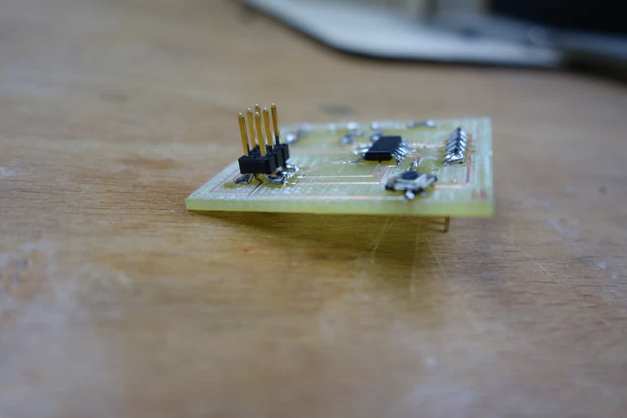
In this weeks Assignment we had to design our own version of the "Hello-World-Board" by adding some components (LED + button).
The process to fabricate this board reaches from designing the schematic and the board over milling it and finally solder the resulting PCB.
We also had to use our lab equipment to observe the operation of a microcontroller circuit board the results can be found on our group-page. We learned how to operate an oscilloscope and how to use it to observe pulse signals and other continuous-signals.
We also had to use our lab equipment to observe the operation of a microcontroller circuit board the results can be found on our group-page. We learned how to operate an oscilloscope and how to use it to observe pulse signals and other continuous-signals.
Tools used
- Soldering Iron
- Solder
- Third Hand
- Flux-Pen
- Solder Wick
- Smd-Pliers
- Solder Wick
- Multimeter
- Sandpaper
- Mantis Compact
Designing the Schematic
To design the schematic I used eagle again, like i did for the ISP. I started by adding the Fabacademy-Library by using this method. Basically you download the library place it in eagles library folder and then include it via the library-manager.If you are using eagle for the first time this Sparkfun-tutorial could be helpfull.
I calculated the value for the resistor the same way as I did for the ISP Leds .
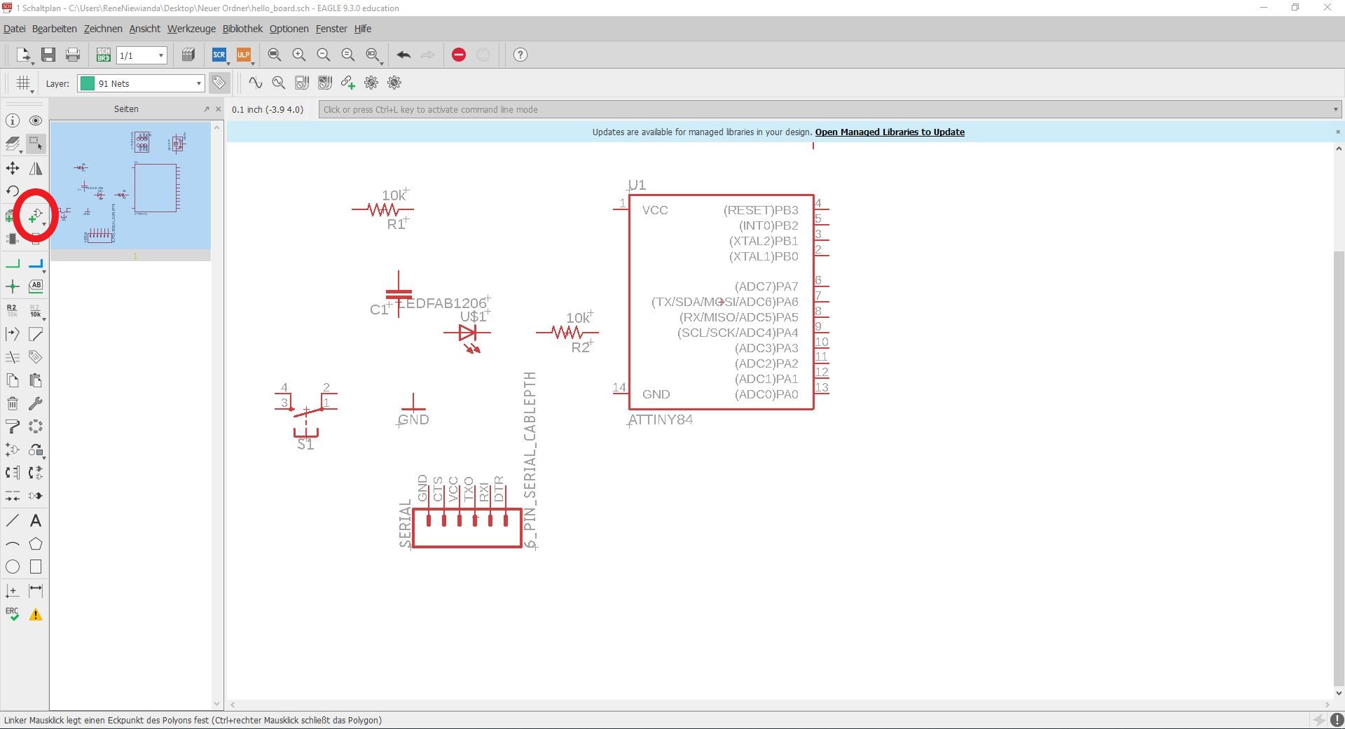
First I added some of the parts i needed for the board by pressing the add-part-Button. When the button
is pressed a list opens where you can choose the part you need. When you have found the part just click where you want to place it.
I could not find a ATtiny44 in the library so I had to use the ATtiny84 for this schematic, since both have the
same pins and footprint it does not make any difference.
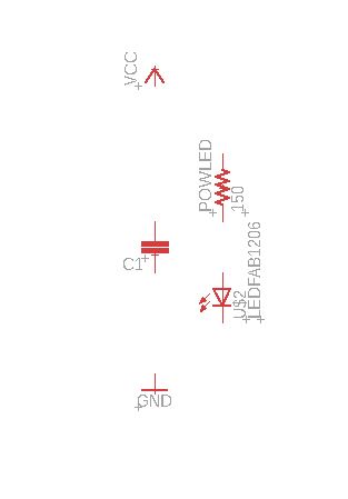
Now I took the parts I needed for the power-indication-led and the capacitor (which protects the microcontroller from voltage spikes)
I aligned the like shown in the picture on the left using the move tool from the toolbar on the left.

I also added names and values to the parts.
You can alter the properties of a part by left clicking and selecting properties.
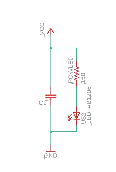
After making sure that all parts were aligned in the right way I began to draw the real circuits by using the Net-tool. Here you should keep the orientation of the parts in mind especially the orientation of the leds.
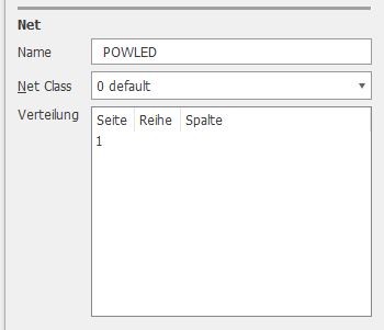
When you now right-click on the green netlines you can name them. This is really helpful later on, when designing the board.
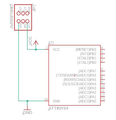
Since the rest of the circuit is more complicated than the small circuit-part shown above
I followed some basic rules, so I do not lose orientation in the process.
First I connected every VCC and GND pin to VCC and GND.
First I connected every VCC and GND pin to VCC and GND.
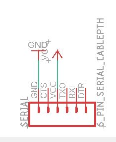
To make the schematic more readable you can add several GND and VCC sourced. When designing the board they all
are mapped to the same subcircuit.
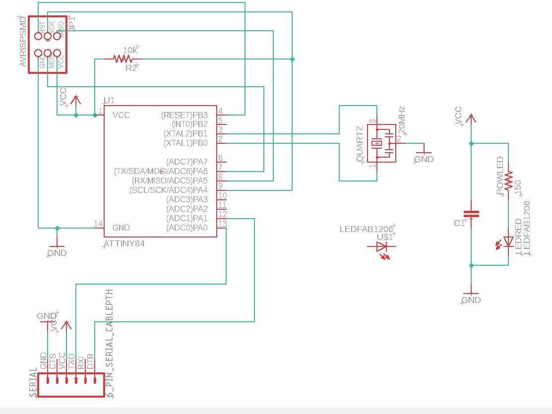
Now I connected all the pins of the ATtiny to the respective pins of the other parts using the given Hello-World-Board as orientation.
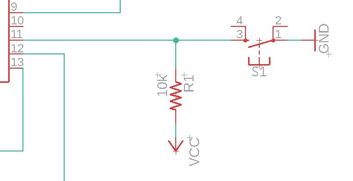
In the next step I added a button and pullup resistor to one of the free pins of the Attiny.The resistor is necessary so no shortcuts are produced.
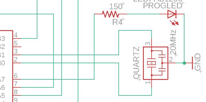
After the button I added an LED and a resistor to another free pin. The resistor is necessary so the led wont be damaged by high currents.
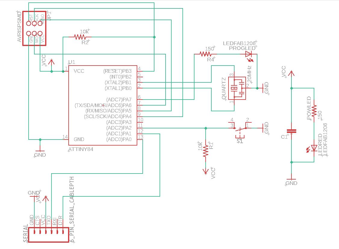
Lastly I checked if everything was connected in the right way and named the subcircuits in the process. I found a tiny mistake in the upper left corner:
I connected VCC to the SCK-pin and not to the reset-pin which could have damaged the microcontroller, if did not catch this mistake.
Designing the board
Now it is time to design the board itself. Other than in the ISP-Assignment I will use the build in autorouter that eagle offers. To switch to the board view simply press the corresponding button at the top-toolbar.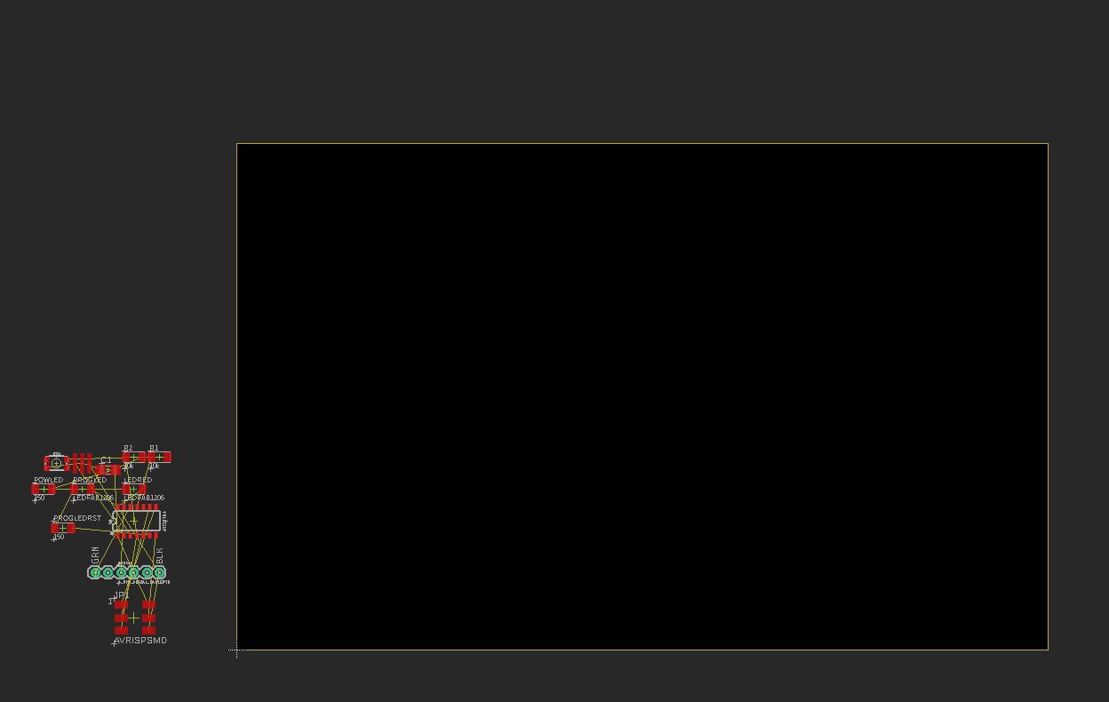
When I first opened the board-editor it looked like this. All parts are crumbled together in the bottom corner.
The yellow lines indicate which pins have to be connected.
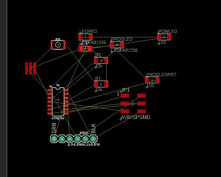
I roughly placed all the parts on the PCB. I placed them a little bit random and a little bit like the Hello-World-Board layout.
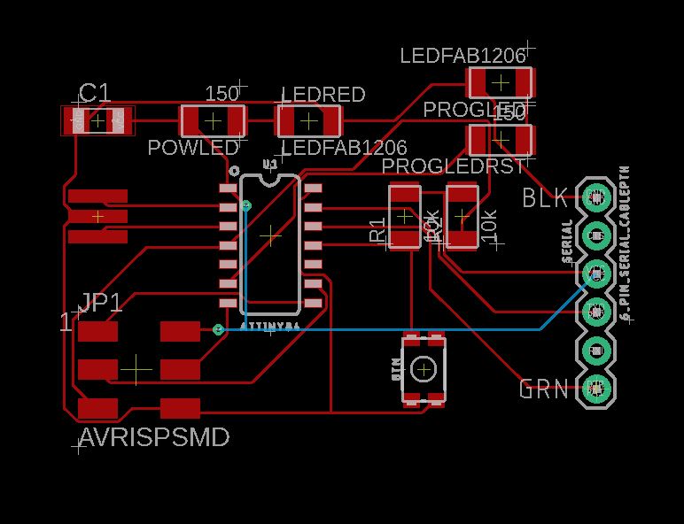
Then I started the autorouter (tools->autorouter). It took several attempts and rearrangements till i got this layout.
the blue lines are lines on the bottom layer of the pcb.
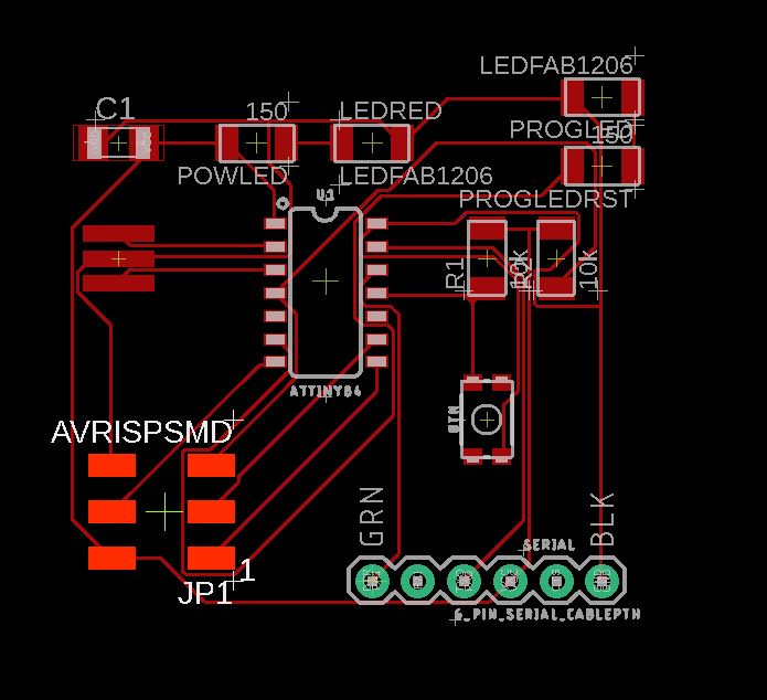
Since I do not want two sided PCB, I manually rearranged some connections by hand.
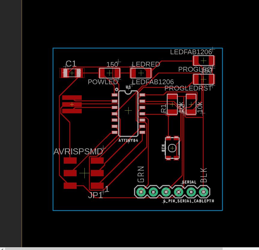
Now I drew the boundaries of the board. First with blue lines like shown on the picture, which is wrong because
blue lines indicate things on the bottom layer. Then I replaced it with the right (yellow) lines.
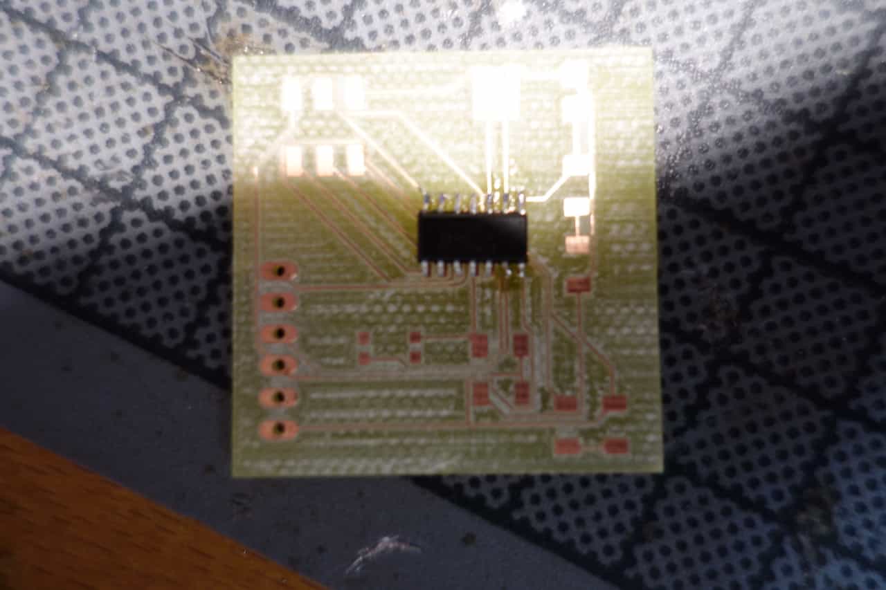
I milled this board but while soldering I saw that some of the copper connection where broken on the PCB.
This happened because I choose a line width which was too thin to be milled correctly. So I had to redesign the board.
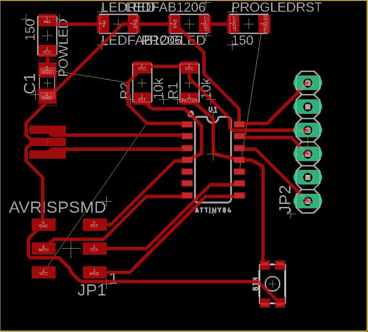
After adjusting the line thickness in the net-properties and a lot of rearranging I came up with this layout.
As you can see there are still some yellow lines which means that not everything ist connected like i should be.
This happened because I removed the bottom layer which was added by the autorouter.
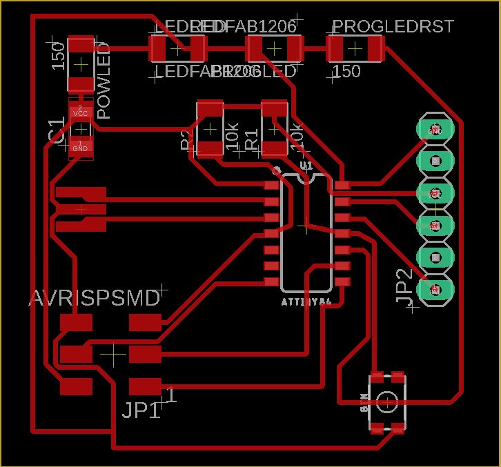
To get my final board-layout I had to redraw the last connections by hand. Finally i came up with this design.
Milling the PCB
Since I used the same Mill and technique for the ISP the instructions are the same and can be found here.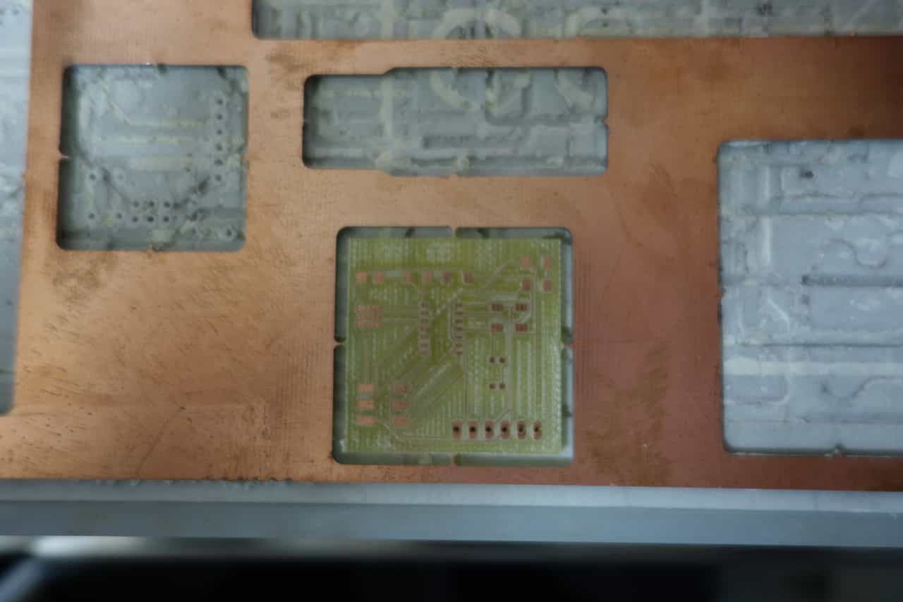
A short comment on Design rules
Eagle provides two checkups to see if your board has any major errors:- The ERC (electrical rule check) which checks for open or overlapping pads and wires it also creates warning when you forget to assign a value to a part
- The DRC (design rule check) which checks your trace widths and component spacing
Another example is when you make pads that intersect with the border of the PCB then the DRD produces an error. But sometimes you want to do that to save some space since pinheader-pads for example are sometimes bigger then the need to be.
Soldering the board
This is my second time soldering smd components, so this time I was a lot faster and more precise than the last time with the ISP.I left the clock unsoldered because this board is made to program an button and an LED so no external clock is needed.
To ensure good soldering joints: First clean the tip of the iron with the sponge and the metal-wool inside soldering stand. Now heat up the the pad and the pin of the part you want to solder. Then add enough solder to cover the pad and the pin of the part. Wait a second then remove the soldering iron. For smd-components first only heat up the pad and add solder like described above. Then put some flux onto the joint. Now take the smd-component and heat up both the joint and the connection of the component. Wait a second then remove the soldering iron. If you are using solder with lead then you know a joint is good when its shiny.
Throughout the whole process I used a Multimeter to make sure that no shortcuts or unwanted connections where created. If I detected a shortcut I used the soldering wick to fix it.
Components used
- 1x ATtiny44
- 1x 100nF SMD Capacitor
- 1x 2x3 SMD Pinheader
- 1x red SMD LED
- 1x white SMD LED
- 2x 150Ω Resistors
- 2x 10kΩ Resistors
- 1x SMD Button
- 1x 1x6 Pinheader
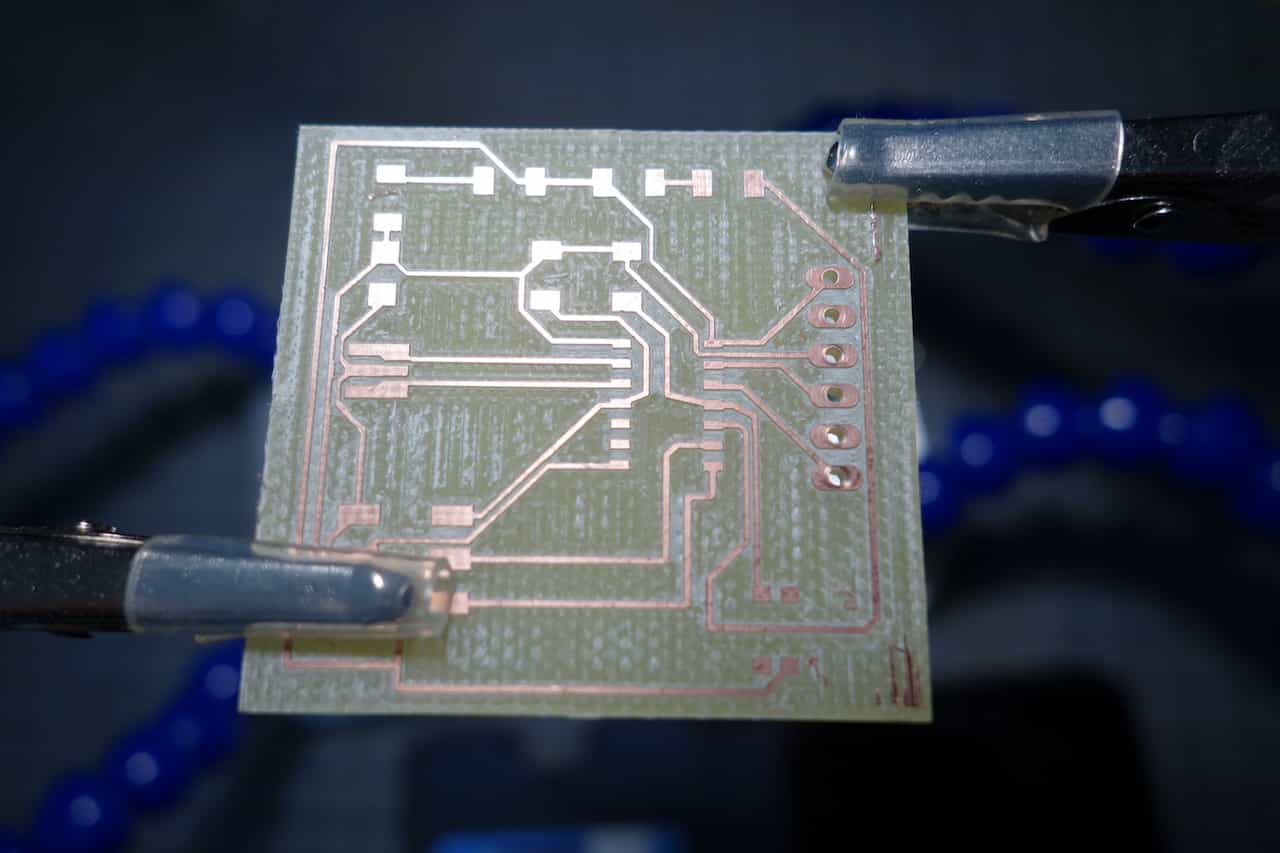
First I checked the whole PCB if it was correctly milled. And non of the connections was broken.
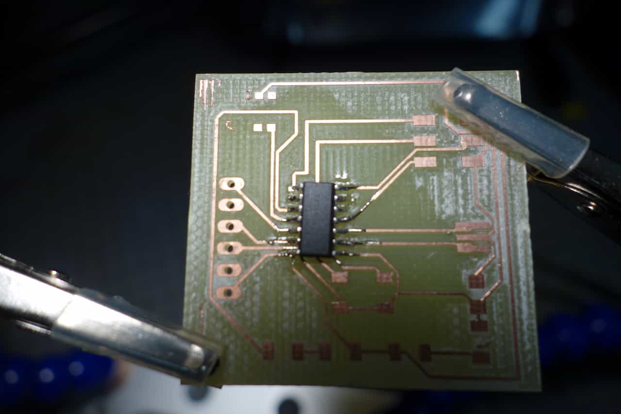
Like for the ISP-board I soldered the ATtiny first. Since it hast the thinnest legs and therefore the highest probability of screwing up.
The indent of the microcontroller should be at the VCC pin so keep the orientation in mind.
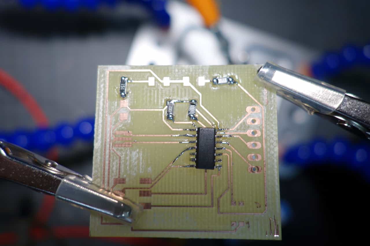
Next I soldered the 4 resistors. Be careful that you place the right capacitor onto the right pads.
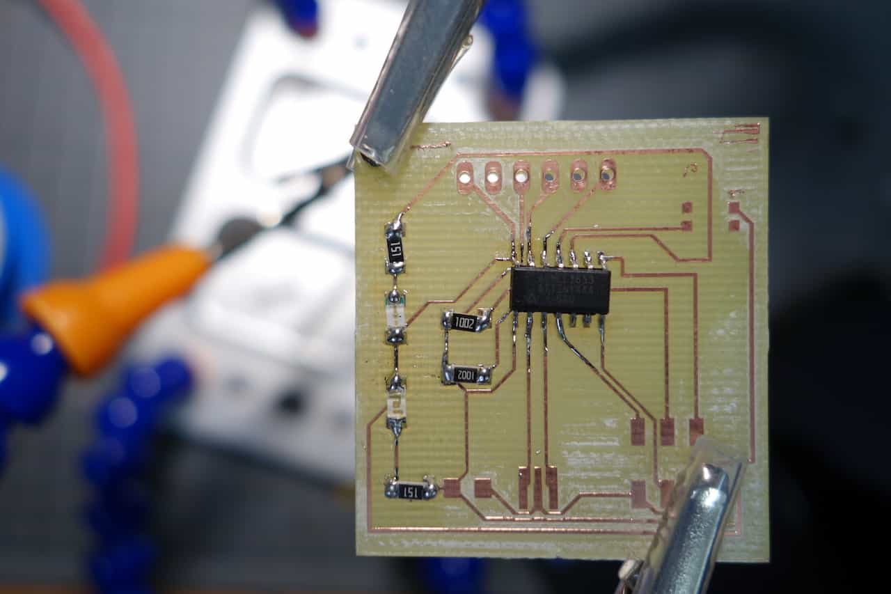
Now is soldered the leds. I used my multimeter to determine how they must be placed. Here GND is in the middle of the leds.
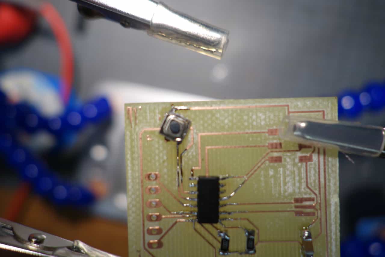
Since we did not have a fitting smd button and I did not want to start from scratch I hat to improvise.
I soldered don the button in a way that no shortcuts where created and it will still work as intended. As you can see on the picture is soldered a little bit diagonally and the two unused pins are removed.
I soldered don the button in a way that no shortcuts where created and it will still work as intended. As you can see on the picture is soldered a little bit diagonally and the two unused pins are removed.
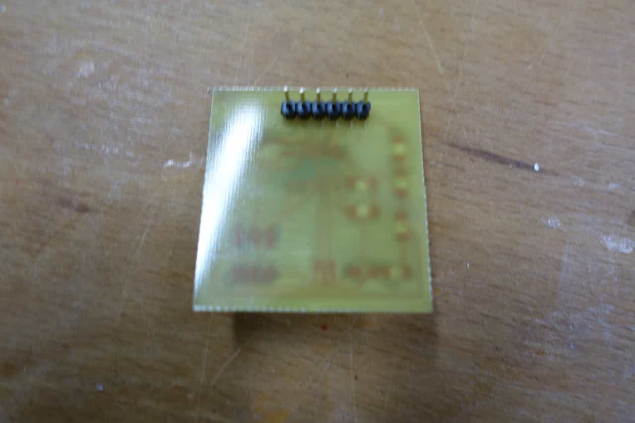
Lastly I soldered the bottom and top pinheaders.
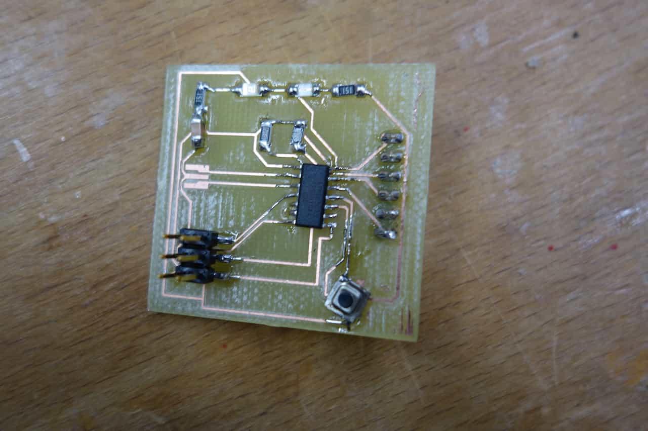
After everything was soldered I checked again for shortcuts. After that the board was finished.
A video of the working board can be found in the Embedded Programming Assignment
A video of the working board can be found in the Embedded Programming Assignment
Favourite beverage of the Assignment
I took ill recently, so fennel-tea it is.