Week 5
Electronics Production
We were introduced into PCB production and the materials and components used for the process. This week's assignment was to characterize the specifications of the PCB production process and to make an in-circuit programmer by milling the PCB and then to program it, and to start using it.
Characterizing the specifications of the PCB production process
The proccess can be summarised in four steps.
1. Design
In addition to the placement of components and the network of connections (Traces) between the components, the circuit design should also take account of the size of components, for ensuring proper placement and easy soldering.
On the macro level, the design should be in tune with the shape and size of the final device which will accomodate the PCB. To make the final device more compact and to reduce the consumption of PCB Blanks, it should only occupy the least space.
On the micro level, the design should also account the capabilities of the machine available to mill the board. The clearence between the traces ought to have a minimum width, for the end mill to go in between the traces and remove the copper. The traces should be having sufficient width to pass the required quantity of current, failing which the current will dissipate as heat and the PCB could get fried up. It should also take account of the possible noise (disturbances in signal) and the components should be placed such that the noise level is kept to a minimum and does not interfere in the smooth functioning of the PCB.
Several softwares like Kicad, Eagle etc can aid in making the schematic layout of the circuit and then to turn it into a PCB design. The design file has to be exported as a high resolution monochrome image in PNG format so that it can be imported into the "Fab Module" software which will drive the milling machine. The machine will make the mill/drill/cut along the border line distinguishing the black and white in the monochrome image.
2.Milling, Drilling & Cutting operations
The milling, drilling and cutting operations are done using the "Fab Modules" software. During the milling operation, the PCB blank is milled such that the copper left over will make the traces. After the milling operation, the drilling of holes (if required) is done followed by a cut to obtain the desired final shape (and size) of the PCB. The machine we have at our lab is "Roland MDX-20". The head of MDX-20 which accomodates the spindle can move in three directions, and the bed can move in the Y direction. The machine has physical switches to move the head (which accomodates the spindle and the end mill) along the vertical axis making it possible to set the origin on the Z axis. Another physical button "View" pauses the running operation, and brings the base plate to the front, making it possible to inspect the copper blank in between the operation.
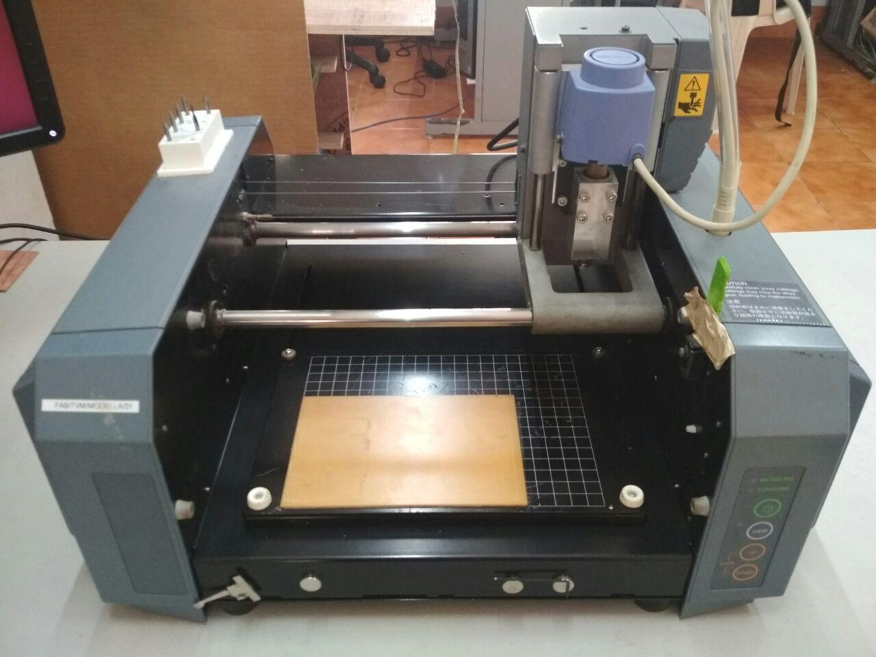
The Orange Buttons on the right bottom side of the image are the buttons to move the end mill in the vertical direction. The Button above is the "View" button. The sacrificial layer can be seen mounted on the base.
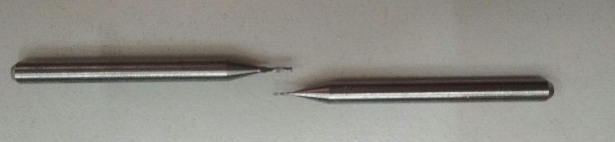 The above image shows the 1/32 & 1/64 end mills (bits having the diameter of
the cutting end as 1/32 & 1/64 of an inch respectively). The 1/64 bit
is used for milling to make the traces and the 1/32 bit is used for making the drill/cut.
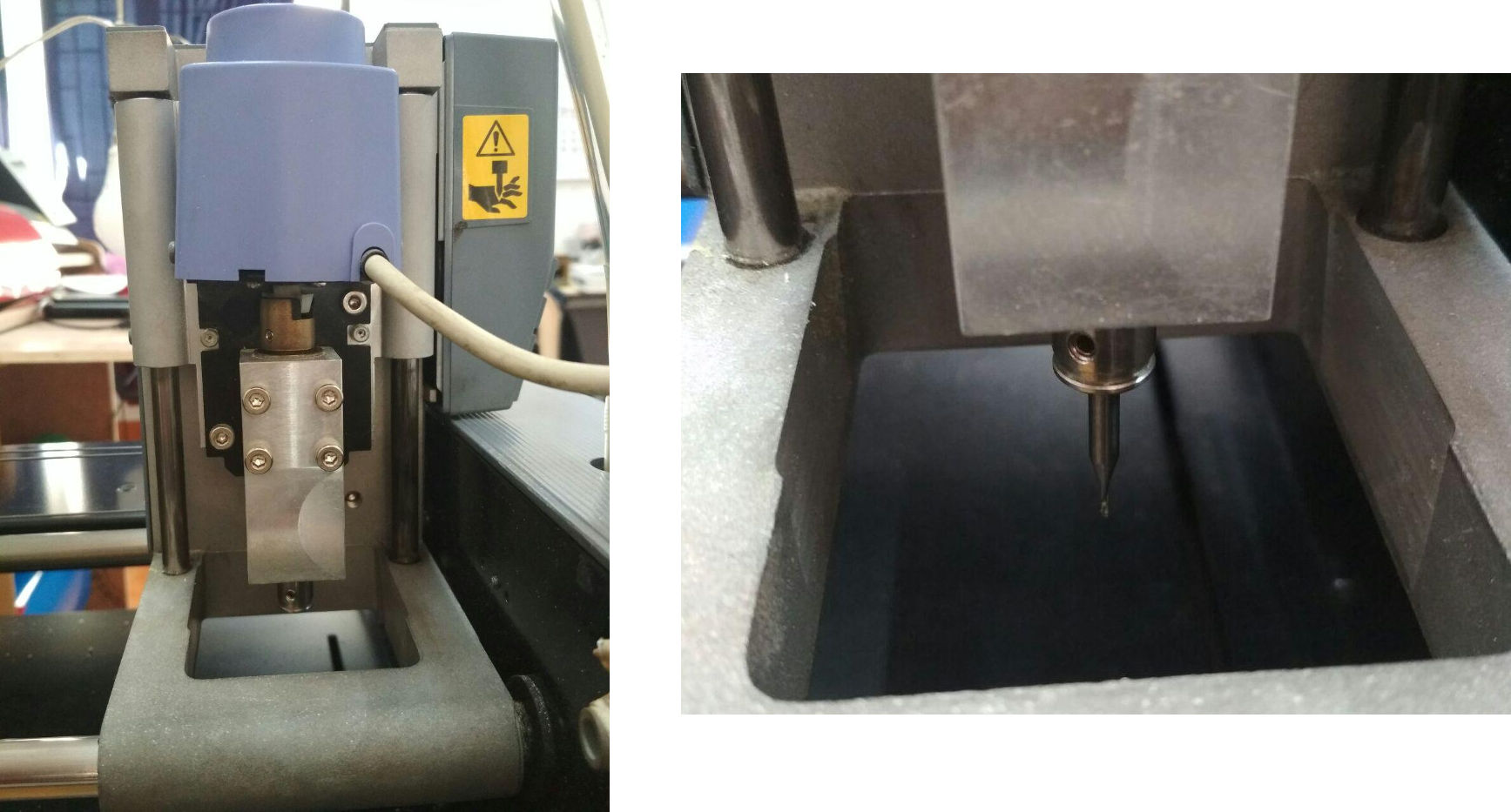
The end mill is to be mounted
and tightened to the machine by turning an allen key bolt.The end mills should
be mounted such that a sufficient length is inside the chuck. In case of
insufficient supporting length, the end mill can vibrate during the operation
and can break. There is a vertical constrain to the movement of the end mill which
is to be taken account of while deciding the supporting length of the bit.
A closer look of the end mill mount can be seen with and without the end mill mounted.
The small hole for the allen key
is also visible.
The above image shows the 1/32 & 1/64 end mills (bits having the diameter of
the cutting end as 1/32 & 1/64 of an inch respectively). The 1/64 bit
is used for milling to make the traces and the 1/32 bit is used for making the drill/cut.
The end mill is to be mounted
and tightened to the machine by turning an allen key bolt.The end mills should
be mounted such that a sufficient length is inside the chuck. In case of
insufficient supporting length, the end mill can vibrate during the operation
and can break. There is a vertical constrain to the movement of the end mill which
is to be taken account of while deciding the supporting length of the bit.
A closer look of the end mill mount can be seen with and without the end mill mounted.
The small hole for the allen key
is also visible.
The machine bed has to be first inspected for any bends and deformations. If any bends are observed, the copper blanks should be mounted away from the deformed areas. If the blanks are mounted on an uneven surface, the depth of milling and cutting will vary across different areas and can result in an improper operation.
The next step is to mount the sacrificial layer atop the bed, over which the copper blank will be mounted. The sacrificial layer can be mounted using a double sided tape.
The copper blank is then mounted atop the sacrificial layer using a double sided tape. The thickness of the blank is to be measured prior to mounting, so that the depth of cutting needed can be ascertained. The thickness of double sided tape is also to be taken care when fixing the depth of cutting for easy removal.
After mounting the copper blank, it is time to install the 1/64 end mill and configure the machine for milling operation using Fab Module. With respect to the placement of the copper blank, the origin of the machine is to be set in the X and Y directions using Fab Module. The origin on Z axis is to be set by using the up and down arrow keys provided on the machine, and the zero'ing of the bit is to be done such that the bit rests on the blank.
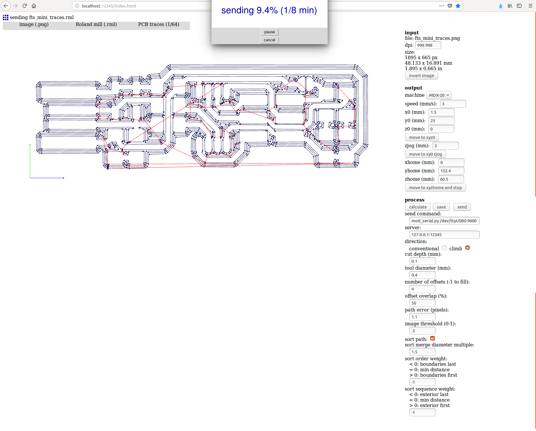
The traces image file is to be imported into Fab module and the output is to be selected as Roland Mill(.rml) and the tool is to be set as PCB Traces (1/64). Speed of cut, cut depth, the number of offset (from the boundary of black and white, towards the black) to be performed and overlap between the offset's etc can be set in Fab Module and the milling operation can be completed.
Once the milling operation is completed, the 1/64 end mill has to be replaced with the 1/32 bit for the drilling/cutting operation. The origin has to be kept same as that of the milling operation.
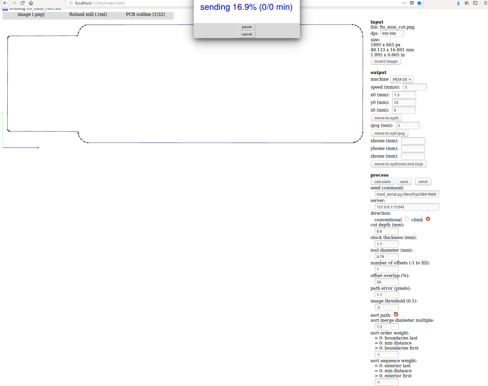
The image file for the "cut" is to be imported into Fab module and the output is to be selected as Roland Mill(.rml) and the tool is to be set to PCB Outline (1/32). Depth of cutting in a single pass, and the stock thickness are to be entered in Fab Module. The machine will calculate the number of passes required for completing the cutting operation. Increasing the depth of cutting in a single pass increases the risk of breaking the bit.
After the cutting operation, the PCB has to be removed from the blank and the debris to be cleared off.
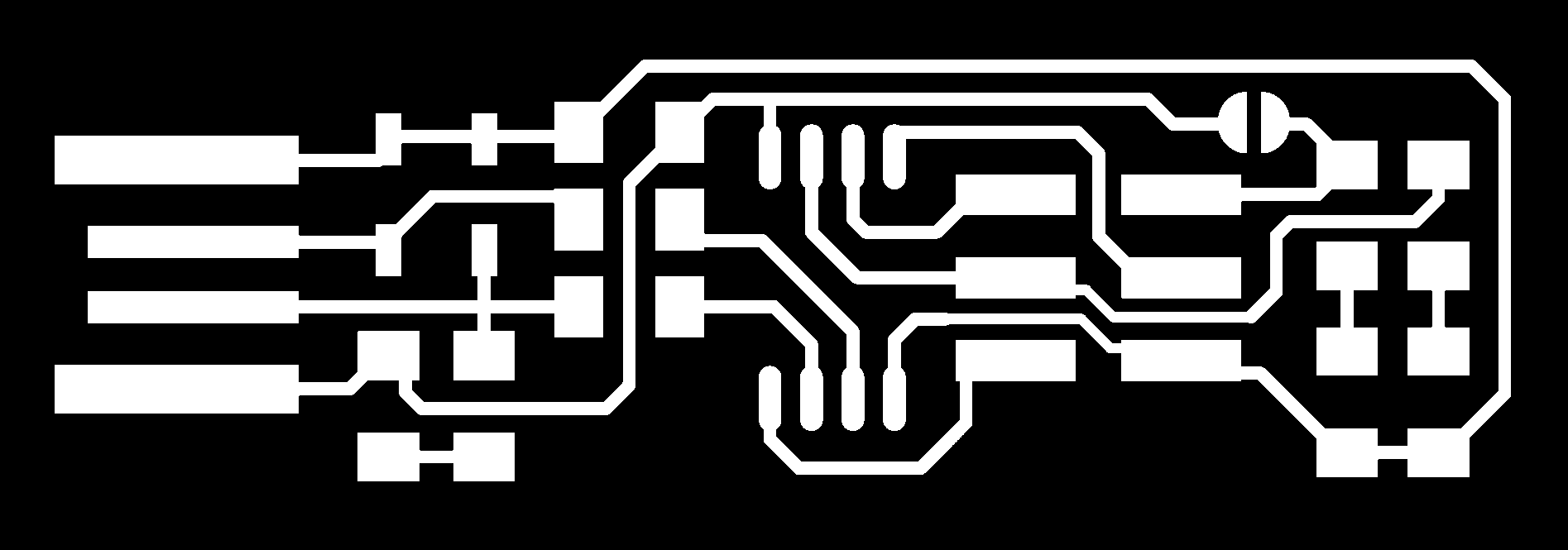
To know the capability of the machine at various trace widths and clearance, this traces image was imported into the Fab Module and milled using 1/64 bit and the result obtained is the image below.
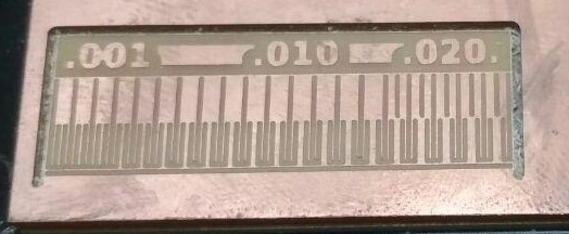
The milling operation was carried out with a speed of 3mm/s, number of offset as 4 and offset overlap at 50%. It was observed that, when the thickness of trace is less than 0.004 inch (0.1mm), the machine gave an imperfect result with the traces being broken at the lower edge. With respect to the clearance between the traces, the machine did not mill out the portions where the width was less than 0.16 inch (0.4mm). The same was obvious to happen for the diameter of the bit was 0.4mm.
It is to be concluded that the trace width has to be kept more than 0.1mm and the clearance between the traces has to be kept at atleast 0.4mm. However, traces with width less than 16 mill have the tendency to break out from the whole during the milling operation. Also, traces with lesser width (<16mill) are also prone to get damaged easily during soldering.
3.Collecting the components and soldering
Soldering each of the components onto the board is the next stage. Since, the components are very small, it is adviced to collect and organise it, as to identify and distinguish each component during the soldering operation. An easy way is to list out the components name on a piece of paper and to stick the components against its name using a double sided tape.
Since each of the components have a safe temperature limit, the soldering is to be done inside the allowable limits as per the data sheet of the component. It is due to this reason, why a soldering station is used instead of soldering iron. A Soldering station gives constant temperature at desired level's.
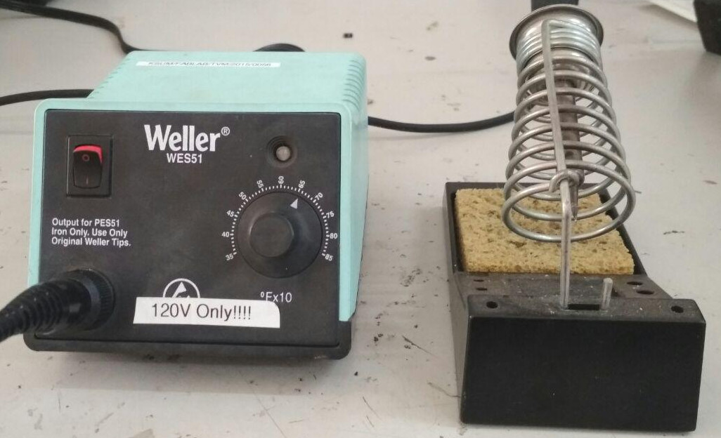
The above image shows a soldering station at our lab. The knob to adjust the temperature and an LED can be seen in the image. The soldering iron is to be kept at the stand and never on the table. The sponge is to be rinsed in water for cleaning the soldering tip by wiping over the wet sponge. After powering on the soldering station, wait for the LED to start blinking, indicating that the temperature is stable at the set value.
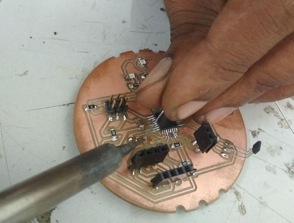
The components are to be soldered in its correct orientation as per the circuit diagram. The soldering has to begin with the micro controller, for the much needed working space that an empty board gives. Solder the other parts in its correct orientation one after the other.
In case a component is to be removed, it has to be done gently without making any damage to the pins of the component and also the traces. The sodler can be removed using a braid which is shown below.
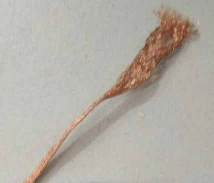
By Keeping the braid spread over the solder to be removed, and by placing the soldering iron above the braid, the heat will melt the solder underneath. A quick pull of the braid will take the molten solder along with it. Alternatively a desoldering pump can be also used for removal of solder at the risk of damaging the traces and the pins of the components.
The components should be resting flat on the PCB surface with the terminals aligned to and touching the copper traces. A good joint will be shiny and will have the least amount of sodler. Heat the copper first and melt the solder over to make a perfect joint.
4.Programming the Microcontroller and Testing
Before starting the programming operation, the board is to be tested for any short circuits and continuity using the multimeter. Also, the placement and the orientation of the components are to be confirmed with the circuit diagram.
Once everything is found good, for programming the PCB, it has to be connected to another working ICSP using an ISP cable. The working ICSP is then connected to the computer though a USB port and the necessary programme is flashed onto the microcontroller of the PCB through the working ISP.
Making of an In Circuit Programmer
I relied upon Brian's website for making an in circuit programmer. The process can be summarised into four stages.
1.Getting the design of the Traces & Board outline images
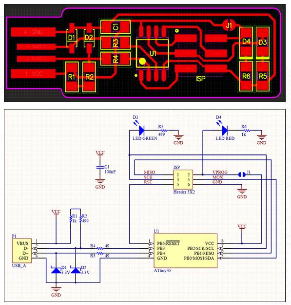
I used the traces and board outline image that is available at Brian's website.

2.Milling and cutting the PCB
The blank has to be first affixed over the sacrificial layer using double sided tapes. For the milling operation, end mill of 0.04mm (1/64") is used and the same was mounted onto the machine.
The next step is to open Fab Module and configure the machine to do the milling operation.
1. PNG image of the traces was imported into the Fab Module.
2. The output format was selected as roland mill(.rml)
3. The tool selected was PCB traces (1/64)
The settings related to the origin were adjusted according to the available area on the blank that was already mounted on the machine. The origin on z-axis was set by moving the drill bit in the vertical direction by using the buttons on the machine. The speed was reduced to 3mm/s from the default value of 4. Below is the screenshot of the entire settings with which the machine made the traces.
After the milling operations where completed, the end mill on the machine was changed to 0.08mm (1/32"). The origin on the x-y axis for the cutting job should be kept identical to that of the milling operation which can be done in fab modules. The next step is to configure Fab Modules to make the cut.
1. PNG image of the cut was imported into the Fab Module.
2. The output format was selected as roland mill(.rml)
3. The tool was selected as PCB outlines (1/32)
The settings related to the origin were kept same as that of millling operation (in my case it was 1.5,25 ). The origin on z-axis was set by moving the drill bit in the vertical direction by using the buttons on the machine. Below is the screenshot of the entire settingss with which the machine made the cut.
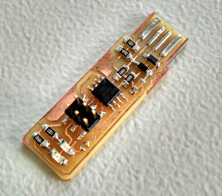
3.Soldering the components onto the PCB.
Before turning on the soldering station, the PCB components are to be collected and arranged so as to identify and distinguish each component during the soldering operation. The component name's were listed out on a piece of paper and the components were sticked against the name using a double sided tape. The Bill of materials used are as follows.
1. Micro Controller - Attiny 45
2. Resistor R1 - 1 KOhm
3. Resistor R2 - 499 Ohm
4. Resistor R3 - 49 Ohm
5. Resistor R4 - 49 Ohm
6. Resistor R5 - 499 Ohm
7. Resistor R6 - 1 KOhm
8. Zenor Diode D1 - 3.3V
9. Zenor Diode D2 - 3.3V
10. LED D3 - GREEN
11. LED D4 - RED
12. CAPACITOR C1 - 100nF
13. ISP HEADER - 3x2
The soldering station was turned on and the temperature was set to 650 Fahrenheit. Each of the components were then soldered onto the board one after the other as detailed in the image below which was obtained from Brians webpage.
After soldering the components, the three lines acting as USB terminal were given an additional layer of lead for getting a fairly tight fit while plugging it into a U.S.B port. The jumper was also bridged using solder.
4.Programming and Testing
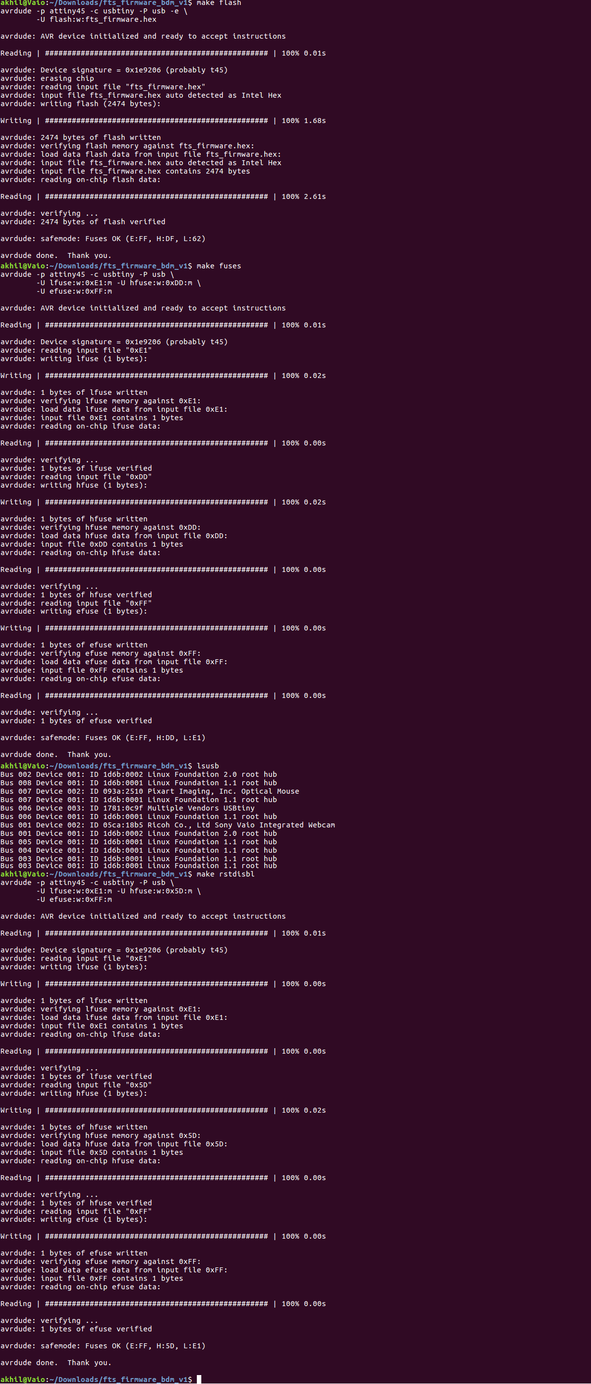
For the the device to act as an in circuit programmer, the micro controller has to be first programmed. Terminal window was opened and the following command was entered
sudo apt install avrdude gcc-avr avr-libc makeThe firmware were downloaded from here and extracted. With the terminal in the directory of the extracted folder, the following command was entered in the terminal.
makeThe device was connected to another programmer (usbtiny) avaialble at the lab using a cable through the 2x3 pin. The programmer was then connected to the laptop through USB cable. With the device connected to the laptop through the programmer, the following command's were entered in the terminal.
make flashmake fusesThe programmer was removed from the laptop and the device. The device was then directly plugged into the laptop and the following command was entered in the terminal
lsusbNow check if the device is listed in the terminal. If usbtiny is listed in the terminal, the device is recognised and ready for programming. The device was again connected to the programmer and the programmer was connected to the laptop through USB. The following command was entered in the terminal to disable the reset switch.
make rstdisblThe screenshot of the terminal window during the operation can be seen below
The newely made In Circuit programmer was tested by using it to programme Amith's ISP which turned out to be successful.
Errors committed
1. Breaking of bit:
After completing the milling operation of my ISP board, the 1/64 bit on the machine was replaced with 1/32 to begin the cut. When installed onto the machine, the shank of the 1/32 bit was projecting out more than what the 1/64 bit did. Without taking account of the additional projection of the shank, i tried to move the bit back to the previous origin using fab modules interface by entering a value of 10mm as the z0 value. However, the drill bit crashed onto the board at the exact origin on the x-y axis and breaking the cutting edge in the process.
It was inferred that, after removing a bit, the machine should be moved to its previous origin without installing the next bit. After moving to the origin, by using the up and down arrow keys on the machine, the next bit has to be installed such that the bit rests on the blank.
2. Wrong orientation of components during the Soldering operation.
While soldering the diode D1 of my ISP board, i soldered it in wrong orientation and had to remove it and resolder in the correct orientation.
To avoid the possible desoldering and the subsequent resoldering, this reminded me to cross verify the orientation of the remaining components before it was soldered onto the board.
3. Improper Cutting during the group assignment.
During the group assignment, the cutting operation was finished with the machine skippin one side of the rectangle. Upon scrutiny, it was observed that the image was not displayed correctlly in the fab module. There was no path on the bottom side of the rectangle and the machine left it out. The image was then inverted in gimp and then again imported into fab module and a second cut was made with the same origin.