Week 15
Networking and Communications
This weeks assignment was to design and build a wired and/or wireless network connecting at least two processors and the Group assignment was to send a message between two projects
A network of MCU's may consists of more than 2 processors. There will be atleast one Master MCU and one slave MCU. The master controls the entire setup and communicates with the slave's. The master sends instructions to the slave's, which perform the instruction and returns the result back to the master. The slave's cannot communicate with each other and there can be many slave's controlled by multiple masters in a single network. There are several networking protocols with which communication can be done between devices. In Serial communication, at one instance, one bit of data is send over a communication channel. The bits of data will be continously send one after the other. Some of the protocols in serial communication are asynchronous communication, Inter-Integrated Circuit (I²C or I2C), Serial Peripheral Interface (SPI), Universal serial USB etc.
Inter-Integrated Circuit (I²C or I2C)
During the output week, it was learned that the LCD display was having 16 pins in total, out of which 6 pins(4 data pin, reset pin and enable pin) had to be mandatorily connected to the MCU. For faster data transfer, the additonal 4 data pins was also to be connected making a total of 10. As a display was proposed to be used in the final project, the search for a simpler alternative ended up in experimenting with I2C. The I2C protocol uses only 4 pins for communication, out of which only two pins had to be connected to the MCU. By just using two pins of the MCU, we can network many devices.
The two bidirectional lines of communication in an I2C network are known as the SDA(Serial Data) & SCL(Serial Clock). SDA is the line for the master and slave to send and receive data and SCA is the line that carries the clock signal.
Some of the useful websites to learn about I2C communications are I2C Info, Sparkfun, Circuit Basics
For implementing the I2C protocol, apart from connecting the SCL and SDA lines of all the MCU's, all the MCU's should also have a common ground. Also, just like the reset pin is pulled up, the SDA and SCL line should be pulled high by using a pull up resistor. The MCU's alternatively pull down the two lines to make the communication.
Network Design & Production
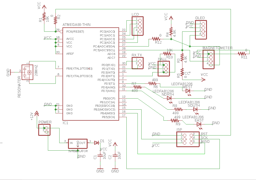
A board was designed with AtMega 328P, keeping in mind of the Final Project. For the need of an interrupt pin for connecting the hall effect sensor, the two-wire bus for i2c, and for connecting the display, ATmega 328P was selected as the MCU. The schematic and board design was made in parallel, which ended up in adding the following components into schematic layout of EAGLE. (More about electronic design during Electronics Design Week.)
1. ATMEGA88-THIN (same footprint as of ATmega 328p) (Package:TQFP32-08THIN, Library: fab).
2. Resonator (Package:EFOBM, Library: fab)
3. CAP-UNPOLARIZEDFAB (CAP-UNPOLARIZED) (Package:C1206FAB, Library: fab) -
Two bypass capacitors are used to fill up the dips and variations in the incoming voltage at
the VCC pin of the MCU.
4. Resistors - RES-US1206FAB (RES-US) (Package:R1206FAB, Library: fab). -
A resistor of 10k is used to pull up the RESET pin of the MCU. Another resistor of
10K is used to pull up the outpin pin of the
digital hall effect sensor. Two 4.9K resistors are
used to pull up the SDA and SCL lines for the I2C communication.
Four 499K resistors are used to limit the current to the four LED's. Four 0 Ohm resistors
were added during the board design to bridge the traces over each other.
5. LED(Package:LED1206 , Library: fab) -
6. PINHD-2X3-SMD (Package:2X03SMD, Library: fab)
7. REGULATORSOT23 (REGULATOR) (Package:SOT23, Library: fab) - for regulating the external incoming voltage to 5V.
8. DIODESOD123 (DIODE) (Package:SOD123, Library: fab) - to avoid voltage flowing to the
regulator when the board is powered up using the ISP cable.
9. PINHD-1X4 (Version 4) (Package: 1X04 (Version 1), Library: pinhead (Version 3) -
Two numbers were used for serving as the connecting pins for two I2C devices,
which requires an SDA & SCL lines in addition to the VCC & GND. Another one was used as a provision to connect
four unused pins of the MCU.
10. PINHD-1X3 (Version 3) (Package: 1X03 (Version 1), Library: pinhead (Version 3)) - for connecting the digital hall effect sensor (A3144)
having an output pin and the VCC & GND.
10. PINHD-1X2 (Version 3) (Package: 1X02 (Version 1), Library: pinhead (Version 3)) - one for connecting the external power
and another one for connecting the RXD and TXD pin of the MCU.
Below is the schematic after adding all the components and making the electrical connections. Provision for connecting two I2C devices are kept taking account of the Magnetometer sensor and OLED/LCD that is planned to be used with the final project. There are 4 LED's which will b used in combination to indicate the orientation of the magnetometer sensor. The output of the digital hall effect (A 3144) sensor was connected to one of the interrupt pin of the MCU.
The board design happenned in parallel to the schematics by adding, placing and drawing the traces for each connections. The size of the board was fixed taking account of the size of the housing designed for the Final Project and a circle was drawn in the dimension layer of EAGLE. After adding each components and the electrical connection in the schematic, the placement and traces were adjusted in the board layout. Zero ohm resistors were used to cross over the unavoidable intersecting traces. Below is the final layout of the board.
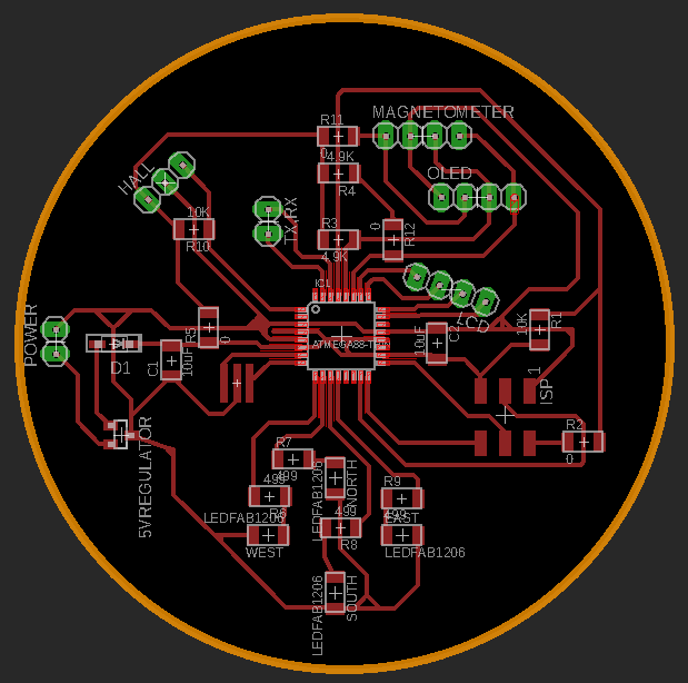
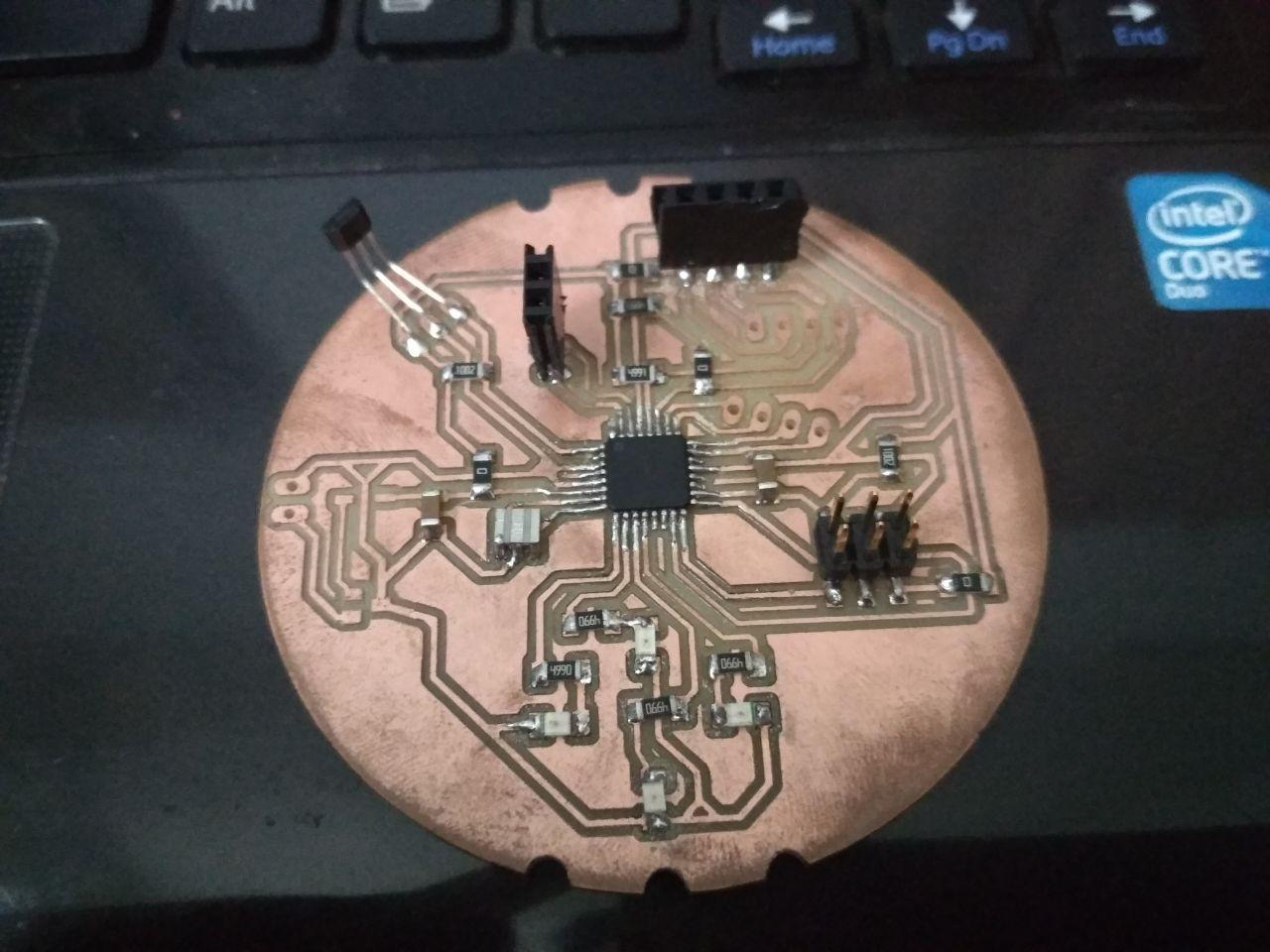
The board design was made with a clearence and trace width of 16mill. The board was milled and cut using Fab Modules and Roland MDX-20. (Read more on Electronic Production & Electronic Design). The final board after stuffing the required components for making the I2C communication is the one below. The hall effect sensor was also soldered along with the pinhead for the I2C device and the LED's.
After making and setting up the final project board, the "Echo Hello World board" made during the Electronics Design Week was connected to the freshly made board thorough the pin head provided by making use of jumper wires. In addition to the VCC & GND, the two SDA and SCL lines were also connected for implementing the I2C protocol between the two boards.
The Hello world board has a button and an LED. The LED on the slave will be powered on when power is connected. The communication to be send was to light up one of the LED in the Final Project board when the button on the Hello world Board is pressed. The Final project board was made as the master and the Hello World Board as the slave. There was no pull up resistor in the Hello world Board for the SCL and SDA pins. Hence, these pins had to be internally pulled up. Below codes were uploaded to the Master and Slave boards using Arduino IDE. (Using Arduino IDE during the Embedded Programming Week.)
Arduino Code on on the Master
  // This programme is written for I2C communication between two baords.
  // This programme is written for the master board.
  // The master board has an LED attached to Arduino Pin 6.
  // The master board request one bit of data from the slave and if the data received is
  // the integer 1, the master will power on the LED and will turn of the LED in all other cases.
  //
  // Akhil Hari 25-06-2018
  // Fab Academy 2018, Fab Lab Trivandrum, India
  // Networking & Communications Week
  //
  //
  // MCU - ATmega 328P (32-pin TQFP)
  // The SDA & SCL Pins of the Master and Slave are connected.
  // The SDA & SCL Pins of the Master MCU are pulled up externally for I2C communication.
  // The Slave board is powered from the Master and shares a common Ground.


  #include <Wire.h>   // Including the Arduino library for implementing I2C.
  int address = 2;      // defining the address of the slave as an integer
  void setup()
  {
    Wire.begin();
    pinMode(6, OUTPUT); // Setting Pin 6 (connected to an LED) as output.
  }
  void loop()
  {
    Wire.requestFrom(address, 1); //one bit of data is requested from the Slave
    while (Wire.available())
    {
      int i = Wire.read();        // Reads the data from the slave and store it in a variable called "i"
      if (i == 1)                 // check if the value received is 1
      {
        digitalWrite(6, HIGH);    // Turn on the LED if value from slave is 1
      }
      else if (i == 0)
      {
        digitalWrite(6, LOW);     // Turn off the LED if the value from slave is not 1
      }
    }
  }
Arduino Code on on the Slave
  // This programme is written for I2C communication between two baords.
  // This programme is written for the slave board.
  //
  // Akhil Hari 25-06-2018
  // Fab Academy 2018, Fab Lab Trivandrum, India
  // Networking & Communications Week
  //
  //
  // MCU - ATTINY44-SSU
  // LED is connnected to PA7.
  // Switch is connected to PA3.
  // PA3 is externally pulled up.
  // Pressing the switch makes PA3 LOW.
  // The SDA & SCL Pins of the Master and Slave are connected.
  // The SDA & SCL Pins of the Slave MCU are pulled up internally for I2C communication.
  // The Slave board is powered from the Master and shares a common Ground.
  // The slave board sends one bit of data each time.
  // When the switch is pressed, the MCU will power off the LED and send the integer 1 to the Master
  // When the switch is not pressed, the MCU will power on the LED and send the integer 0 to the master

  #include <TinyWireS.h>  // Including the Arduino wire library for AtTiny series of processor
  #define address 2           // Defining the address of the slave as 2
  void setup() {              // This is the setup code and will run once
    TinyWireS.begin(address); // Initialise communication
    digitalWrite(4, HIGH);    // software pull up for pin 4
    digitalWrite(6, HIGH);    // Sftware pull up of pin 6
    pinMode(7, OUTPUT);       //LED is connected to PA7. Initialise PA7 as output
    pinMode(3, INPUT);        //Switch is connected to PA3. Initialise PA3 as input
  }
  void loop() {               //This is the main code and will run forever.
    int x = digitalRead(3);
    if (x == HIGH)            // Check the status of Swith. By default, the switch is pulled up externally(In high state).
    {
      digitalWrite(7, HIGH);  // LED on Slave is turned on.
      delay(100);             // Delay of 100ms to account for bounce effect of the switch.
      TinyWireS.send(0);      // Send the value 0 to the master
    }
    else
    {
      TinyWireS.send(1);      // When the switch is pressed, Pin 3 becomes low and sends the value 1 to the master.
      digitalWrite(7, LOW);   // LED on this Slave is turned off
      delay(100);
    }
  }
The SCL & SDA pins of the Master and slave was connected using wires. Also, the VCC and ground for the Slave was provided from the Master Board. The master was powered up using an ISP cable from the ISP programmer. Below video shows the network setup and its working. Upon pressing the button on the Slave, the LED on slave will be powered off and a value of "1" will be send by the Slave. Upon receiving the value of "1", the Master will power on the LED.
Networking more than 2 boards over I2C protocol
To connect more than two boards, all the boards should have a common ground and also the SDA & SCL pins of all the MCU's should be connected to the SDA and SCL line which is pulled up. The schematic diagram for implementing I2C communication between the boards made during the Electronic Design Week and the Input Devices Week and the board made during this week is shown below.
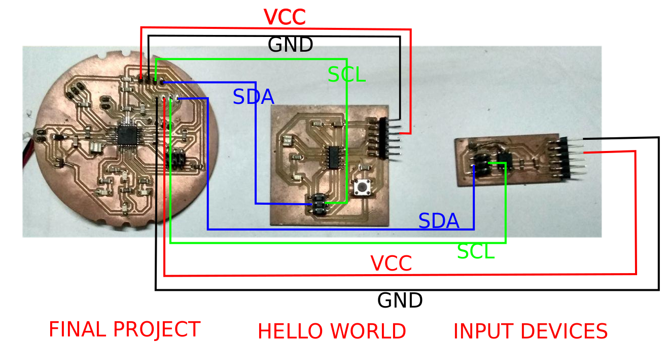
As provisions were already given to connect two I2C devices from the final project board, no modification is required to set up the network of three boards. The network can be powered up through the ISP header of the final project board. The SDA and SCL lines are pulled up in the final project board itself. The Attiny 44 and the ATtiny45 on the hello world board and the input devices board respectively, have the same pin for SCL and SCK. Also, the MOSI pins of the two MCU act as the SDA pin. Hence, the SCL and SDA lines were connected in the schematic to the corresponding pins on the ISP header of the two boards.
For connecting one more board, modification has to be made. The SDA and SCL line has to be split up to accomodate another PCB. The third PCB can be powered up through the ISP header of the final project board, with the final project board being externally powered up. The value of the pull up resistor on the Final Project board might be required to be reduced.
(Implementing I2C communication with an LCD for the Final Project.
UART
In this type of communication, dedicated lines will connect the transmitting and receiving pins of two different micro controllers. The transmitting pin of the master is to be connected to the receiving pin of the slave and vice versa. The board should be individually powered up with a common ground. Different programme are to be flashed onto the Master and Slave Boards.
While writing the programme for either Master/Slave in Arduino IDE, a serial port is to be first created. By using the listen, read, and write functions we can receive and transmit data. Using print and println functions we can print the values to the serial monitor so that we can verify the correct working of the boards by connecting each of the board seperatley to the serial monitor.
I attempted to network and communicate the board's that was created during the Electronic Design Week and the Input Devices Week. I attempted to write a programme which will light up the LED in the "Hello World" board when the hall effect sensor on the Input Week's board detects the presence of a magnet. The Input Week's board will act as the Master which will send serial data to the slave MCU on the "Hello World Board" upon detecting a magnet. The MCU on the slave board upon reciving the serial data will power up the LED. This attempt didnt work and the reason is yet to be figured out.
Arduino Code on on the Master
  // This programme is written for UART communication between two baords.
  // This programme is written for the Master board.
  // This programme has not worked and is to be fixed.
  //
  // Akhil Hari 25-06-2018
  // Fab Academy 2018, Fab Lab Trivandrum, India
  // Networking & Communications Week
  //
  //
  // MCU - ATTINY45SI
  // Output of Hall effect sensor(A1324) is connnected to PB4 (Arduino Pin No. A2).
  // Since, ATtiny 45 doesnt have a hardware serial pin, we have to declare and initialise the serials pins in the software.
  // The default value at PB4 is 512 and the value increases if the south pole of a magnet is brought near the sensor.
  // RXD of the master is connected to TXD of slave and vice versa
  // The MCU will send the value 1, when ever the south pole of the magnet is near the sensor.

  #include <SoftwareSerial.h>
  SoftwareSerial serial(0, 1);  // Initialize serial port to slave MCU on pins PB0, PB1 (RXD, TXD)
  void setup() {
    serial.begin(9600);         //Initialize Serial port to slave and initialize serial communication at baud rate of 9600
  }
  void loop() {
    int x = analogRead(A2);             // Read the analog value at PB4
    if (x > 512)                        // Check if south pole of the magnet is near the sensor
    {
      serial.print("Magnet Detected");  // Prints onto serial monitor
      serial.println(x);                // Prints the analog value on the next line
      serial.write(1);                  // Send the value 1 over serial communication to trigger the slave MCU
      delay(500);                       // Delay of 500 ms in between the readings
    }
    else
    {
      serial.println("No Magnet");      // Prints onto serial monitor.
      serial.write(0);                  // Send the value 0 over serial communication.
      delay(500);                       // Delay of 500 ms in between the readings.
    }
  }
Arduino Code on on the Slave
  // This programme is written for UART communication between two baords.
  // This programme is written for the Slave board.
  // This programme has not worked and is to be fixed.
  //
  // Akhil Hari 25-06-2018
  // Fab Academy 2018, Fab Lab Trivandrum, India
  // Networking & Communications Week
  //
  //
  // MCU - ATTINY44-SSU
  // LED is connnected to PA7.
  // The Slave board is powered from the Master and shares a common Ground.
  // The slave board upon receiving the Value 1 from master will blink the LED.
  // Since ATtiny 44 doesnt have a hardware serial pin, we have to declare and initialise the serials pins in the software.
  // RXD of the master is connected to TXD of slave and vice versa

  #include <SoftwareSerial.h>
  SoftwareSerial mySerial(6, 4);  // Initialize serial port on pins 6, 4 (RXD, TXD)
  void setup() {
    pinMode(7, OUTPUT);           // Set pin 7 as Output
    mySerial.begin(9600);         // Initialize serial communication at baud rate of 9600.
  }
  void loop() {
    mySerial.listen();            //
    int mag = mySerial.read();    // Read serial data on pin 6, and store into variable mag
    delay(100);
    mySerial.println(mag);        // Print mag value to serial monitor via ftdi cable
    if (mag == 1) {               // Check if the value from slave is 1.
      digitalWrite(7, HIGH);      // Turn the LED on
      delay(200);                 // Wait 200 ms
      digitalWrite(7, LOW);       // Turn the LED off by making the voltage LOW
      delay(200);                 // wait 200 ms
    }
  }
  mag = 0;                        // reset serial variable
  delay(100);                     // wait 100 ms
  }