Fabricating PCB
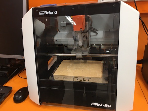
Jari Pakarinen, Fab Lab Oulu staff and Fab Academy 2017 alumni, gave us the local lecture about PCB fabrication. There are several techniques to create PCB. As examples of the techniques of subtracting, vinyl cutting copper sheet, laser cutting and milling circuit board. As examples of techniques of adding, painting with conductive ink, sewing with conductive thread (E-textile) and plating for mass production. For this week’s assignment, I used milling machine to fabricate PCB. PCB consists of layers of different materials. Milling machine removes copper layers from the board to create paths and pads with remaining copper layer. We have Roland SRM-20 in Fab Lab Oulu.
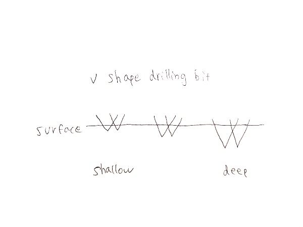
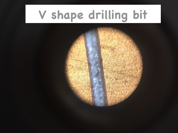
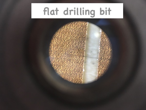
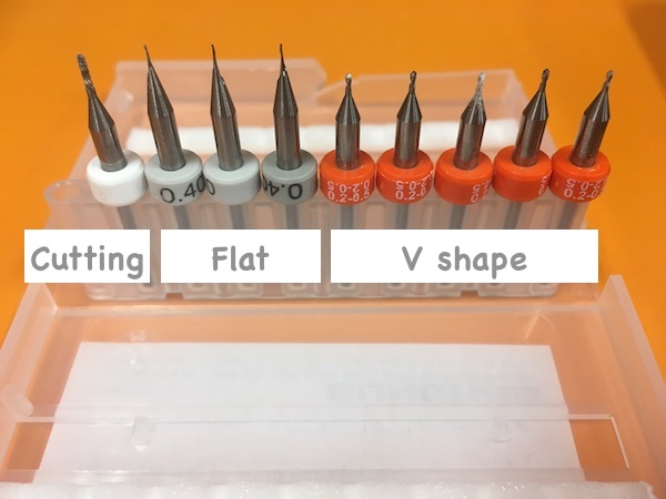
As a milling bit, it is possible to use both flat bits and V-shape pointed bits. The diameter of the flat bits is 0.4mm, the diameter of v shape is from 0.2 at point to 0.5mm at upper. I used V-shape pointed bits.
To fabricate PCB, we need to prepare file as a specific format for the milling machine. For Roland milling machines, file should be prepared as .rml format. It is possible to convert the file in Fab modules.
Converting files
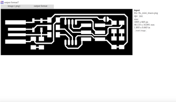
First, I downloaded PNG files of Trace and Outline from Brian's website. I went to Fab modules to change the format of the files for PCB fabrication with Roland SRM-20. I imported PNG file of trace by selecting input>image (.png). The image appeared on the screen.

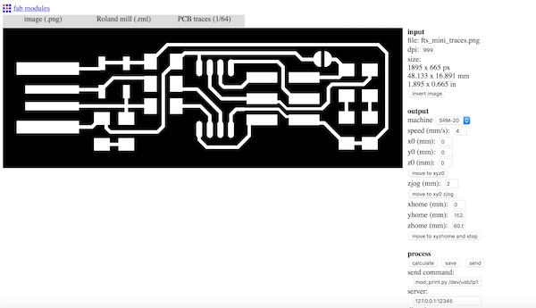
I selected Roland mill (.rml) as output format and PCB traces 1/64 (0.4mm) as process.

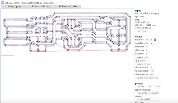
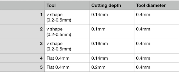
On the right of the image, there are sections where I can change settings for manufacturing. In input section, I can check the size of the PCB and change dpi. With Roland SRM-20, it removes copper layer around the parts which are shown as white in the PNG image. If the image shows opposite colour, I need to invert the image. In output section, I chose SRM-20 as machine and set x-, y- and z- position as 0. Here I can change, such as cut depth, tool diameter, offset, etc. The milling machine repeat following the tracing paths according to the settings. I can also set offset overlap (%), which decides how much the bit overlap the trace paths in each time. I used 0.13mm for cut depth and 0.4mm for tool diameter. I clicked “calculate” in process section, then it showed the tracing paths.

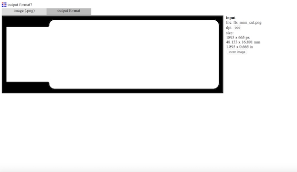
I saved the file as .rml format by pressing “save” button. Next I converted outline image. I chose PNG image for outline as input and Roland mill (.rml) as output format.

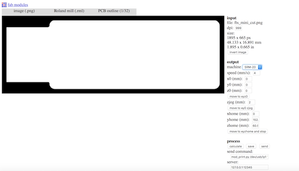
I selected outline 1/32 (0.79) as process. As I did for the trace file, I selected SRM-20 as machine and set x-, y- and z- position as 0.

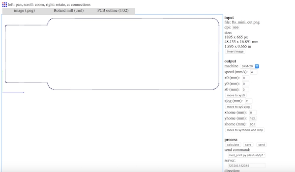
I set cut depth as 0.6mm, and stock thickness as 1.7mm. The thickness of the board is 1.6mm, so with setting thickness as 1.7mm, it will be definitely cut. With this settings the bit cuts 0.6mm in each time, and will repeat three times till it cuts out 1.7mm thickness. The tool diameter can be set a little bit smaller than actual tool diameter. The offset will be divided into both side of the outline, so if I set tool diameter smaller than the actual one, it cuts out more than the machine expects. If the components are placed close to the outline, it causes problems but “cheating” machine a little bit is sometimes useful, for instance when I get error of calculating outline by Fab Modules recognising it is too close to cut. But this time I set tool diameter as 1mm which is actual tool diameter. I pressed “calculate” and saved the file as .rml format.

Settings for milling machine
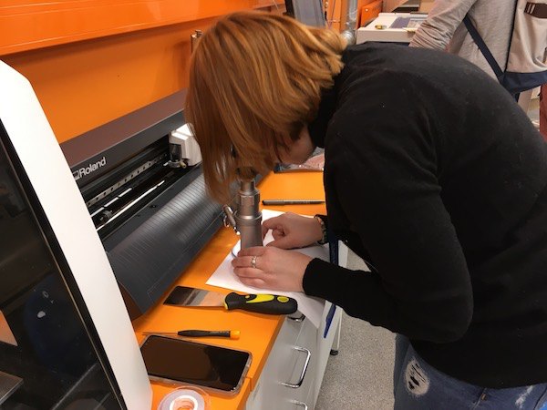
First I fixed the position of the board on the wooden board with double-sided tape. Copper layer of circuit board is about 0.03mm, so it is important to keep the board flat when we manufacture PCB. I carefully applied the double-sided tape without overlapping each other.
I placed it near the lower left corner of the wooded board and set the wooden board in the machine using screws.
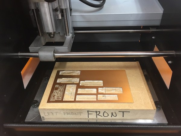
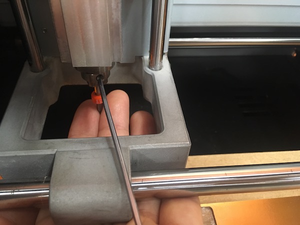
Trace should be done first. I attached 0.2-0.5mm milling bit using hex key.
I opened VPanel for Roland SRM-20 in the computer which is connected to milling machine.
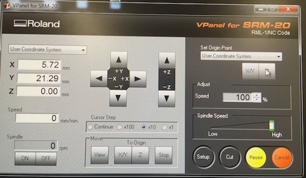
I moved x- and y- position to the lower left corner of the circuit board by clicking the arrows, and pressed “X/Y” button on the right of the screen to set x-, y- origin.
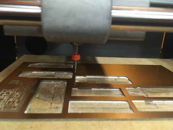
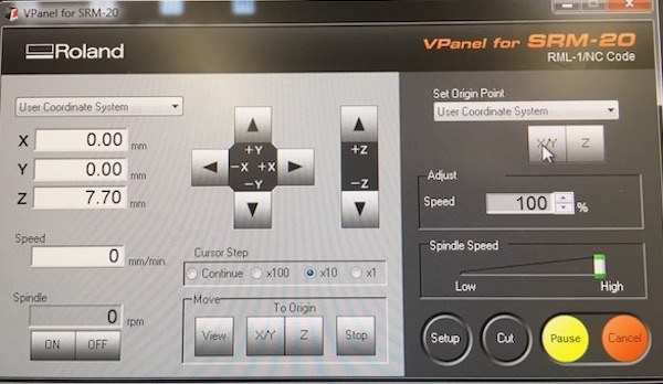
I carefully lowered the z- position till the milling bit came to very close to the surface.
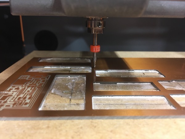
I loosened the screw which hold the bit using hex key and carefully placed the bit on the surface of the board. I fixed the z- position by tightening the screw again.
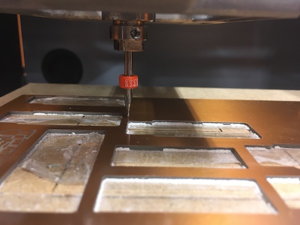
I pressed “Z” button to set z- origin.
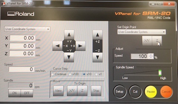
After I set z- origin, I moved z-position slightly higher from the surface to avoid scratching the surface when I started operating. The milling bit can be easily damaged by dropping, so be careful not to drop it!
I pressed “CUT” button in VPanel, and deleted all the previous cutting files. I clicked “Add” and selected the trace file .rml format. I pressed “output” and tracing started.
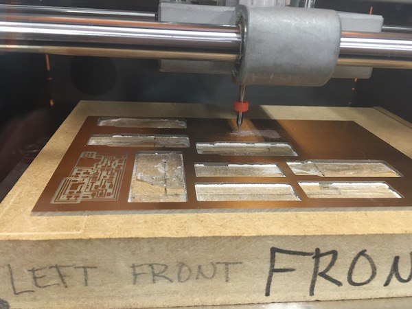
After milling was done, I vacuumed dust on the surface.
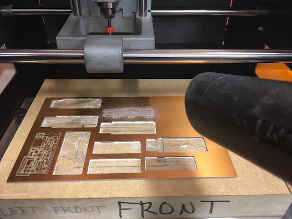
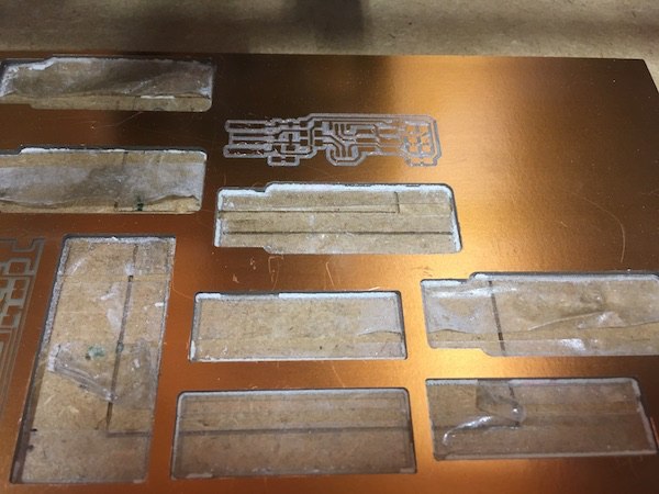
Next I cut outline. I changed the milling bit to flat one for cutting. I adjusted only z- position following the same steps as above. I pressed “CUT” button and deleted the previous file and select outline file as .rml format.
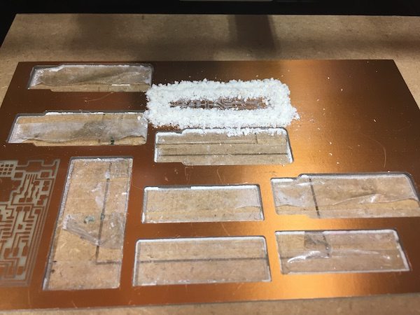
After cutting was done, I vacuumed the dust again. I removed the PCB from the board using the spatula kind of tool.
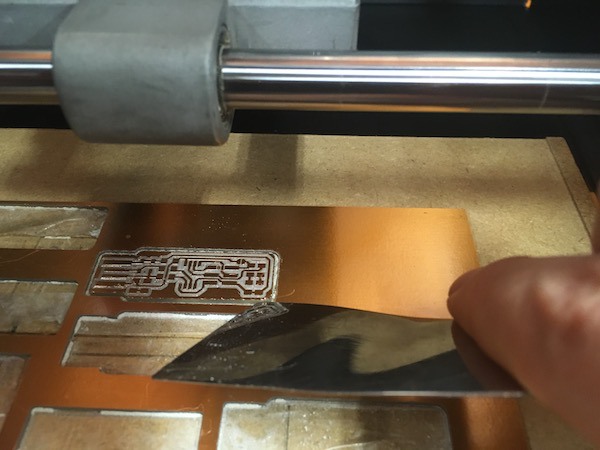
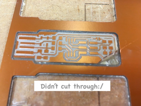
I should always make sure it is cut through before try to remove. Once I tried to remove by force, and broke it. Later I found out the bottom was not cut through. If I had checked and found out it was not cut through before I tried to remove it, I could cut it again from the same x-, y-, z-origin.

Fixing the problem
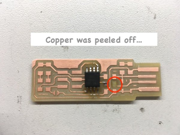
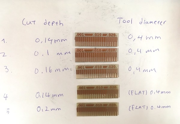
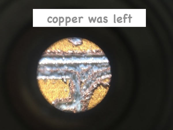
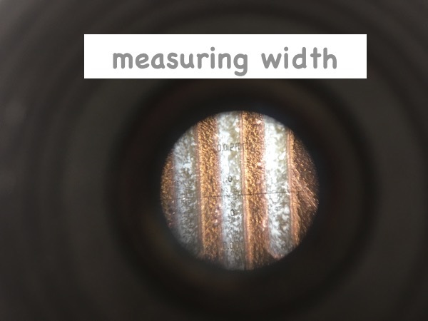
After I checked the board with microscope, I found copper layer was not perfectly removed and tiny copper lines were remained on the PCB. There are several possible reasons:
- When I screwed the bit, I might moved up a little bit z- position from the surface.
- The board was pulled up a little bit when other people took their PCB and I set z- origin on the higher point.
- The machine is not accurate.
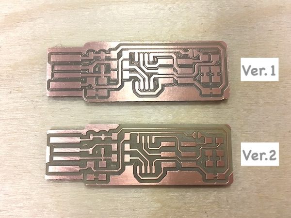
I decided to make a new board with different settings. This time when I converted the file in Fab modules, I changed some settings to make sure it would be milled properly. I changed cutting depth from 0.13mm to 0.14 so that it would trace deeper, and tool diameter from 0.4mm to 0.35mm so that it would trace with more offset overlapping.
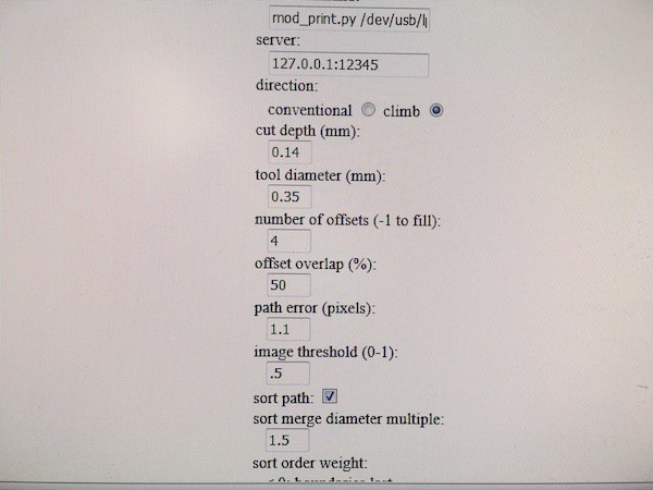
I followed the same steps as above and made new PCB.
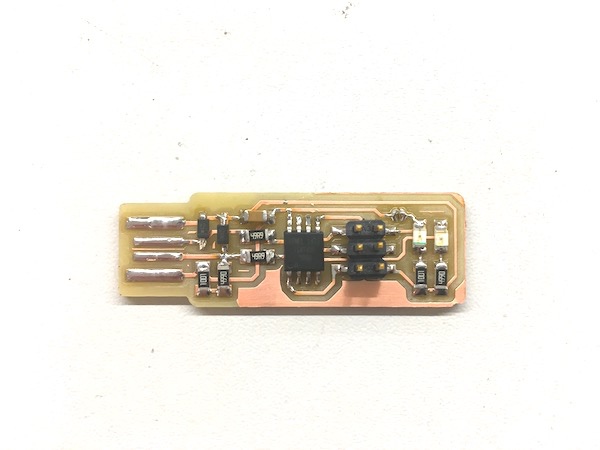
Here is the comparison of two boards. The difference can be seen clearly.
