
Our instructor this week was Antti Mäntyniemi, organized a workshop where we could all: install eagle, add the fab library, create an schematic with all the parts, and then he gave plenty of tips for creating the board and drawing the routes. And then we had the group assignment
To Do
- Create schematic from Neil's design and add led and button
- Prepare board: routing
- Mill and solder components
- Test it (multimeter and programming)
The "Doing"
Designing
Eagle
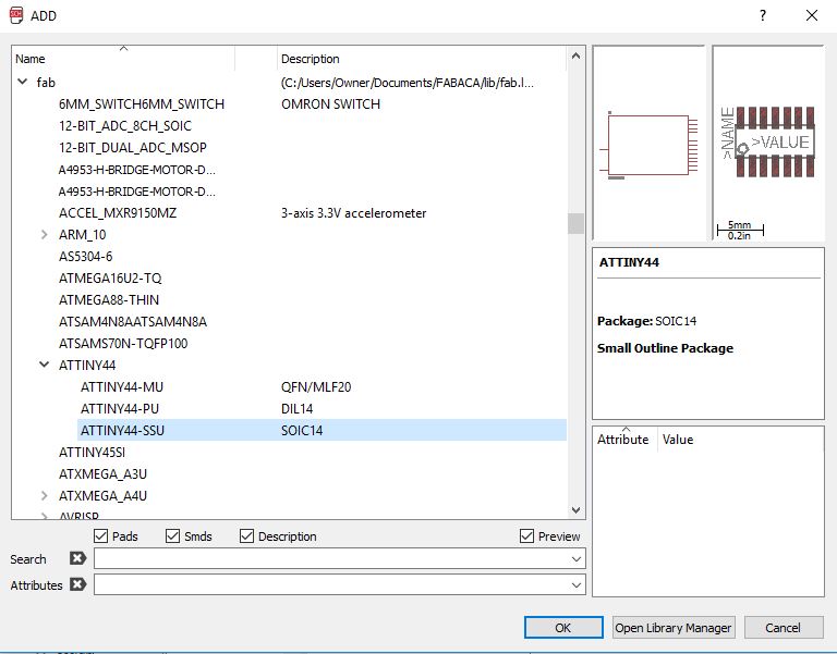
We are going to use Eagle to design the schematic of the circuit. After downloading and installing, it is necessary to add the fab.lbr, a library with the components available in fablabs. To do so, first download fab.lbr to any folder. Then, open the add menu with Edit > Add. If the fab library is not in the list, then Open Library Manager. In this new prompt, browse for the fab.lbr, and then close the prompt. Now the fab library must be in the list

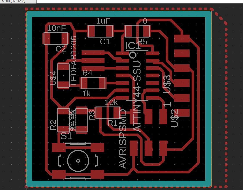
The circuit
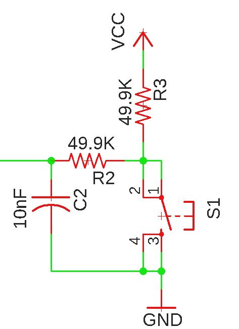
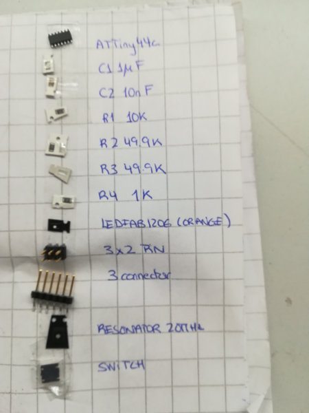
First, it is necessary to understand Neil's image of the circuit: identify the appropiate components and see how they are connected to the rest. Also, we needed to add a button and a Led. Moreover, as a recommendation from Antti, we add a filter that would remove the bouncing from the button (explanation at Antti's assignment and debouncing solution and in the group work assignment). When releasing the button, there is a bouncing that sometimes produces big glitches. It is better to filter those so there are no strange effects in our circuit. This is done with a low pass filter.
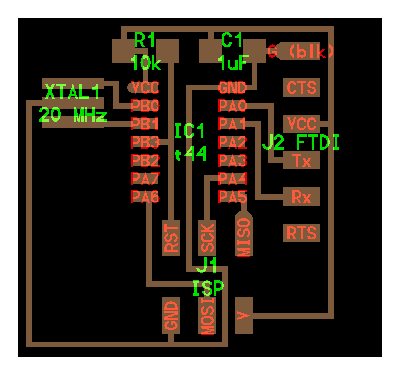

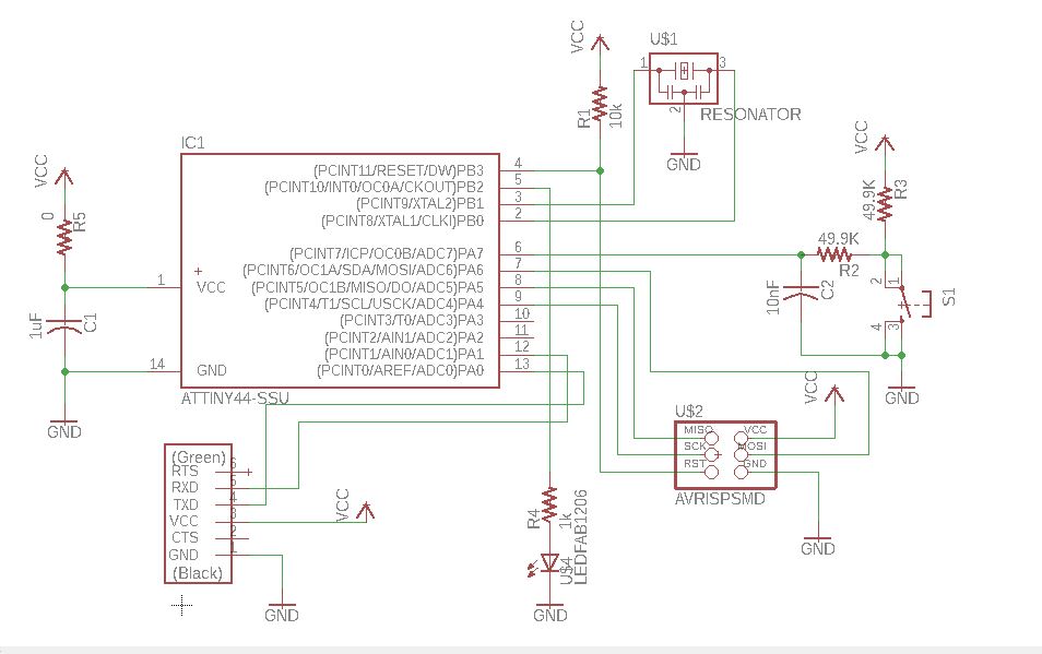
The schematic
Now it's time to create the schematic. We just need to follow the board above and:
- identify the elements (names help) in the board
- get that element from the fab library and place in the schematic
Edit > addprompts the add menu. You have to open the fab lib, and look for the component you need, and clickOk- VCC and GND are selected from supply1 lib
- Place the component somewhere in the schematic. The component can later be moved/rotated
- Press ESC once you are done placing one component
- connect the different components according to the given board and the datasheets if needed.
Draw > Netto draw the connections between components
- Give values to the components:
- rightclick a component to show menu
valueand insert the desired value
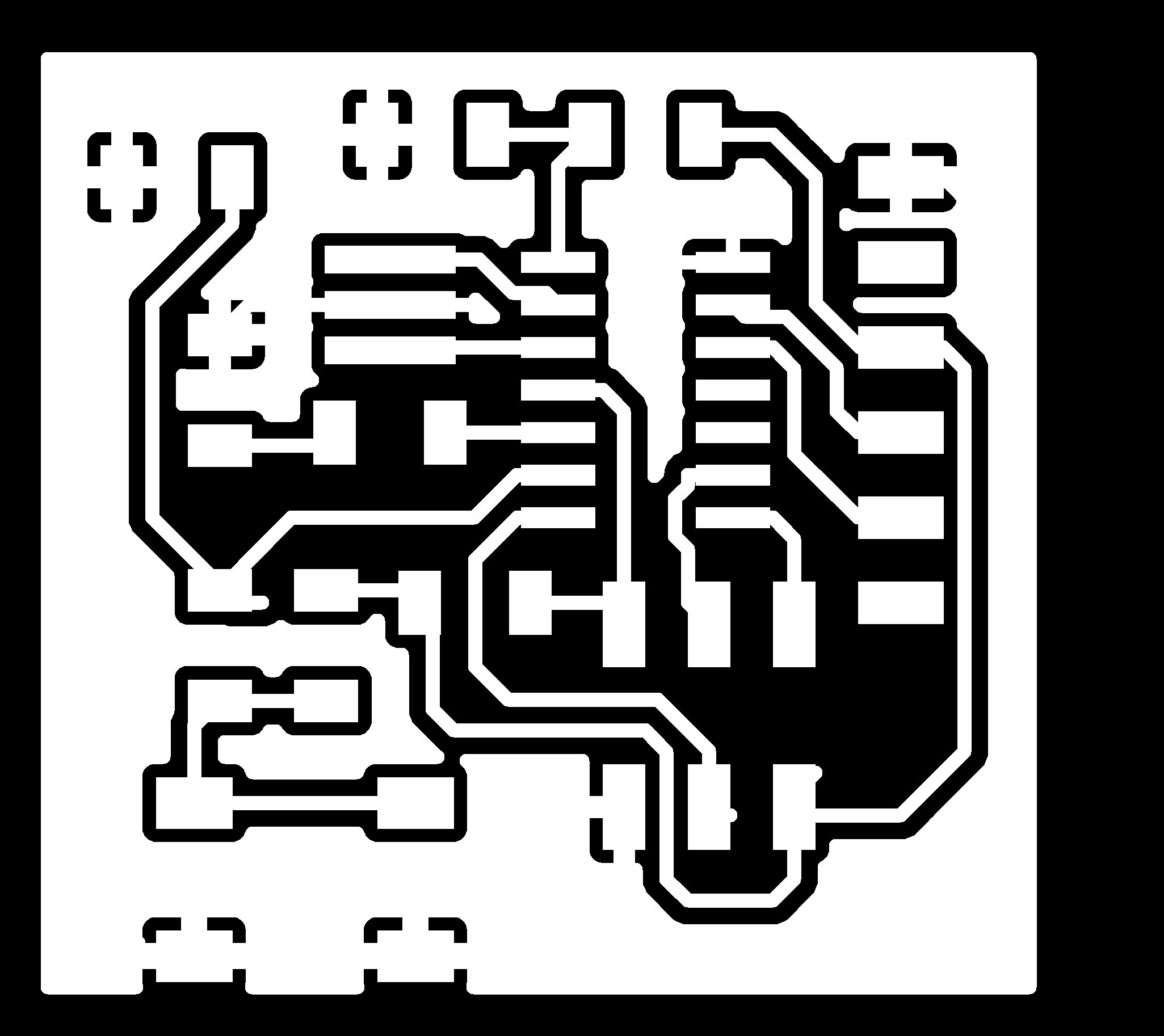
The board
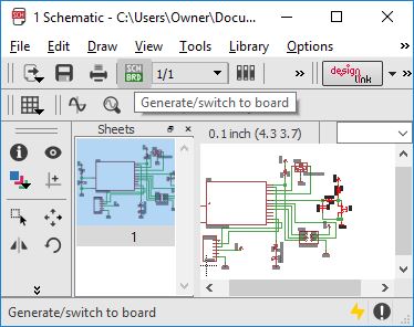
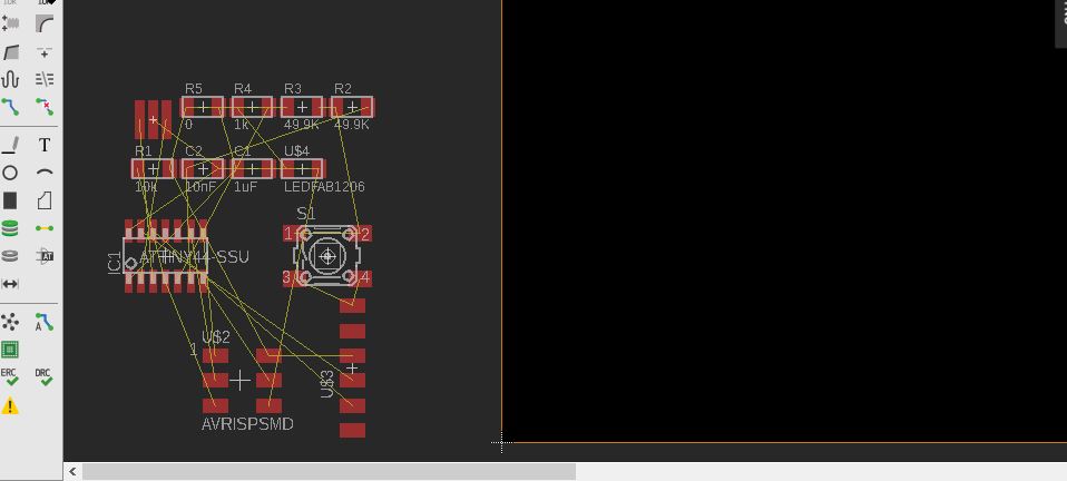
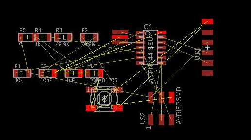
Once the schematic is ready, it's time to create the real traces. First, we need to press Generate/switch to board button to get the board. It is a representation of the board components joined by airwires.
Edit > moveandEdit > rotateto positionEdit > Routeto create routes from one component to another
Once you select route, and click on one component, you get feedback on all the possible endings of the route as seen in the figure on the rightEdit > ripoutto delete a routeTools > ratsnestto reorganize airwires
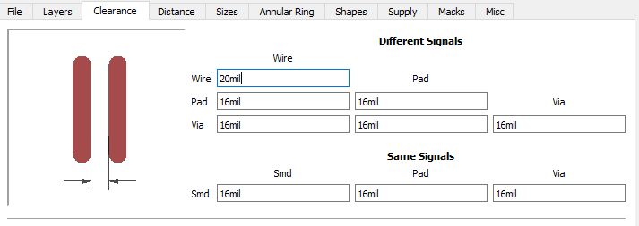
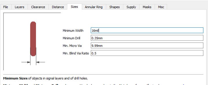
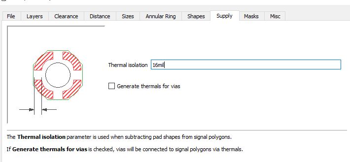
DRC , which will give feedback on possible problems. You can also define your own rules in the DRC prompt, as minimum clearance (space) between conductive elements. You can define new values and save those settings for later usage. Values defined are
- All values for clearance set to 16mill but between wire and wire that is set to 30mill
- Minimum size set to 16mill
- Thermal isolation set to 16mill
Ground layer
To define ground layer as the remaining copper in the board:
Draw > polygon: Draw a polygon around your boardEdit > Name: Name it GNDTools > ratsnest: To put wires to ground layer
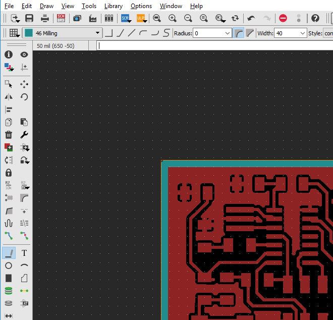
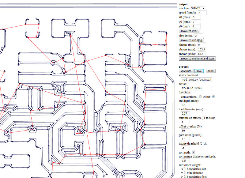
The outline for cutting was drawn in layer 46 (milling) with
Draw > Line, setting the width to 40
Milling and Soldering
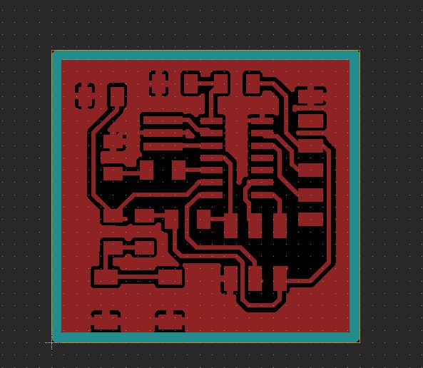
traces and outline
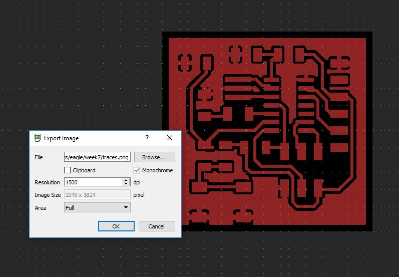
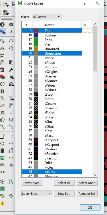
File > Export > Image, with correct whites and blacks. Note that:
- for my settings, for the outline image, the background must be changed to white (Select white at
Options > User interface> Layout) - for the outline, you need to see just the layer 46: milling
- for the traces, you need to just see the layer 1: top
- select monochrome
- set resolution. In this occasion I set it to 1500dpi. UPDATE! it is better to 2400dpi


milling and soldering
I proceeded as in assignment 05 for milling and soldering the board.
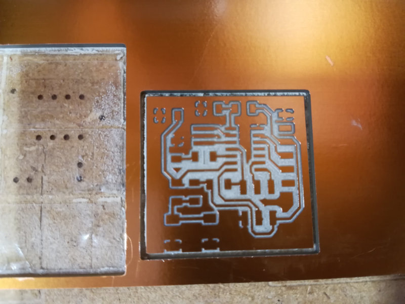
- I used the multimeter to check there was continuity when it had to be and no shortcuts with the board just cut
- I used the multimeter again after soldering the components to check the same thing
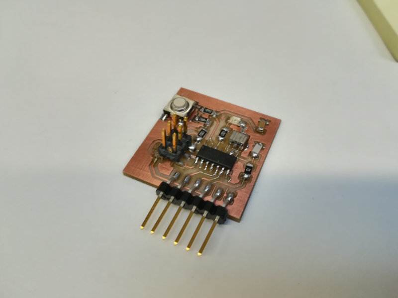
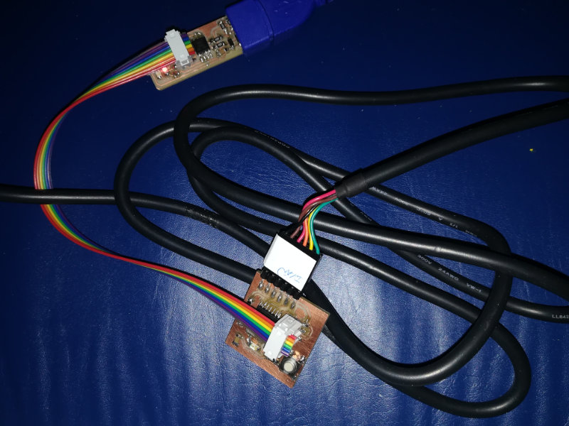
- In this case, I had an "issue" (big issue): I managed to break one of the pads from the board when soldering. With Jari's help, I managed to sold it back. (It is the big drop of solder in the 3x2 pin header that is visible in the picture beneath)
Testing
Programming
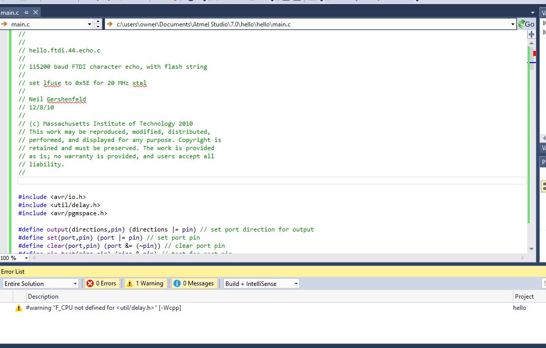
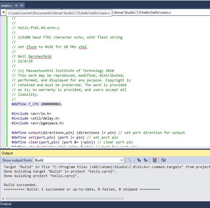
I downloaded the hello.ftdi.44.echo.c. I also downloaded AtmelStudio as I decided to use it as ide following Antti's recommendation.
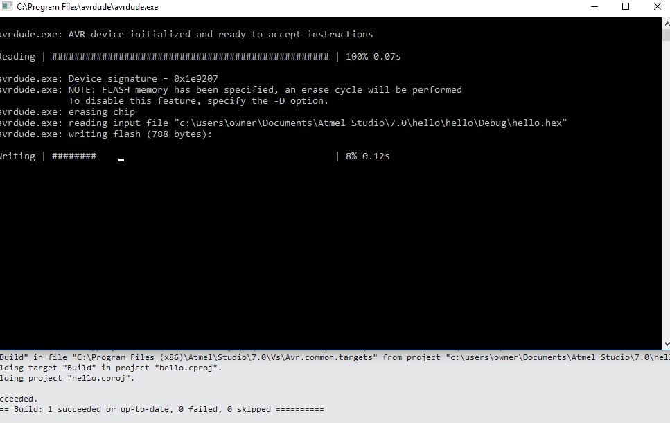
I built Build > Build solution the hello file and got a warning
 I used my programmer from assignment 05 to program this week's board
 In the hello file, it says
 set lfuse to 0x5E for 20 MHz xtal. I programmed the fuses from the command line
avrdude -p t44 usb -c usbtiny -U lfuse:w:0x5E:m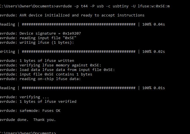 Then, following the link from Antti's, I configured ATMel Studio to work with avrdude as an external tool

Tools > External Tools > Add- Title: name of this configuration
- Command:
avrdude.exe, with the complete path - Arguments:
- -c parameter specifies the programmer being used
- -p parameter specifies the microcontroller (search the avrdude.conf file to find this)
- -v parameters make sure the output is verbose, so I can check if anything goes wrong
- the $(TargetDir) and $(TargetName) are Atmel Studio variables pointing to the project folder and the hex filename
-c usbtiny -p m328p -v -v -v -U flash:w:$(TargetDir)$(TargetName).hex:i - Initial directory: Path to avrdude instalation
- Click
OK
Tools > avrdude. It runs quite fast (TIP: uncheck the close on exit), but I managed to capture the following
 Just need to test if it is working as expected!
Running the program
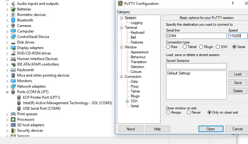
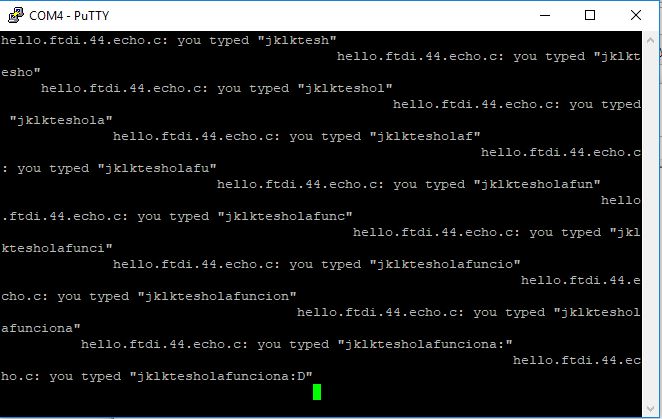
After connecting the board to the computer with an FTDI cable, I checked which is the serial port assigned: COM4.
Then, I opened PUTTY terminal and created a session for serial, with Serial line COM4 and speed 115200, which is the baud given in Neil's hello file.
Resources
- Eagle
- Antti's page
- ATtiny44a datasheet
- B3SN switch (6x6) datasheet
- AtmelStudio
- hello.ftdi.44.echo.c file
- hello.ftdi.44.echo.c.make file
- Components from fabinventory
- fabmodules
- Milling machine
- Configure avrdude as external tool for AtmelStudio
Once done
Summary
- I have learnt to use eagle to design my board: create schematic, route the board
- I have used the multimeter to check my board connections
- I have used the oscilloscope for some basic testing
- I have used my programmer from assignment 05, and it works (!!)
Difficulties
- ...soldering.... again....
Learnings
- From others experience: always check continuity with the board
Tips
- For routing, just start doing it! It gets easier as you go on with the job