Electronics Design
Week 7
This week is one designing with electronic components. For me, this will be the most difficult to learn because I have no background on the subject.
Configuring the software
We will be using Autodesk's Eagle for designing software and configure it for our need with Fab Academy's part list.
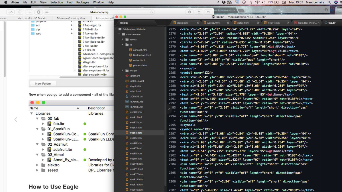
First, we have to point our browser to Fab Academy's turorial page. We install or update Eagle. We then download the refered schematic. Or tried. The link was dead and I had to search the web to find it. I copy-paste the filename and founded the missing file. It was a raw file, perfect for selecting all with crtl-a, then in Atom copied (crtl-v) and saved the file (ctrl-s) in the appropriate Eagle directory.
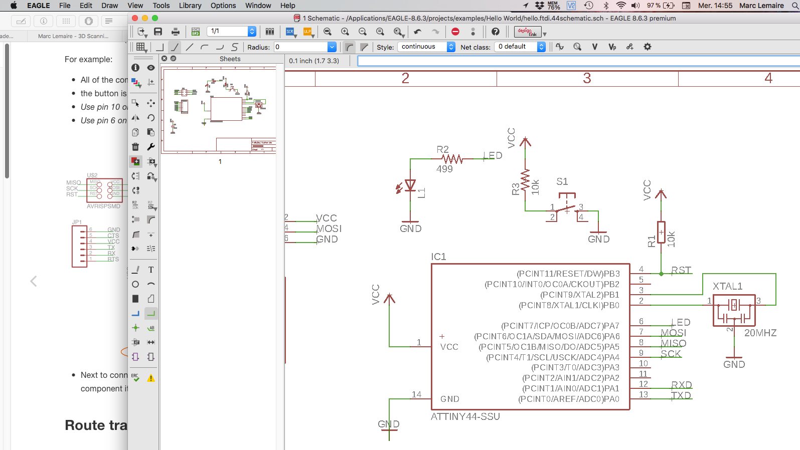
I then opened Eagle and clicked on the project file and read along. Although not being an expert at electroncis, I'm familiar with the symbol used to described electronic components (ground, led, resistors etc).
I then downloaded the Fab Academy's component libraries and repeated the previous process.
As noted before, Eagle was opened. I was seeing my schematic to modify but I was puzzled by the interface. I was clicking around and wondered why I couldn't modify my file. I asked around and learned that I must *double click* on the file to open it. And the software open another window in which we have access to the schematic and can make the appropriate modifications. I must add that at this point, I was working along with Geoffroi and we were helping each other during this initial steps in electronic design.
We then added our first components and I had to ask questions about the locations of components like: "Where are the resistors in the libraries?", in the "Res-Us" folder (Having checked the description column on the right would have spared me this embarrasing moment). I then learned to use the command toolbar on top to add components (two resistora, a diode, a button plus the connection) on the schematic sheet.
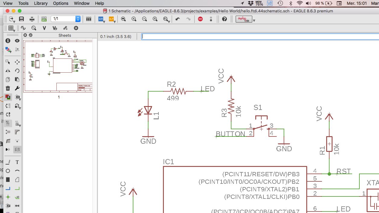
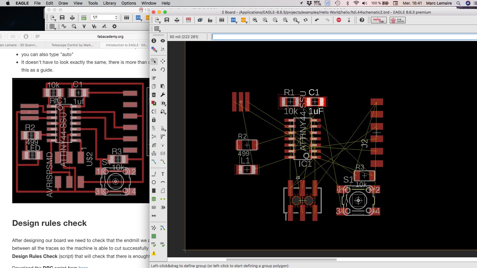
I added the connections (or traces in Eagle) and double checked the connections. Once I was satisfied, I then started the board view. A new interface came up, and I had to move the components in preparation for the creation of the printed circuit board. I place them as suggested, made a few adjusments for the configuration of the traces. As indicated, I downloaded the Design Rules Check, a program that ensure that the endmill will be able to trace the board. I press the DRC button, configure the DRB for one side printed board and fire away.
Almost there: 92.3%. With this results, I can't make it. If I go ahead, I will need to make a bridge with a 0 ohm resistor. Since this is a first try, I have to change the position of my components to a more uptimal setup.
In which the author of these lines try very hard not to loose his patience
So I almost complete this week's assignement. Almost there. Stuck at 92.3% of efficiently. To have the 100%, I have to make two bridges. I deduced that this exercice is more about debugging and working with the software than anything else. So, bridges are not ok. For such a simple circuit, I'm sure that there's no need of it. So I test and move around the components and see the results. Stil no luck.
A learning curve is always hard to climb. It's a black hole where time don't have any meaning really. You're stuck and want to find a solution and be done with it As Soon As Possible™.
I'm really stuck. I start to search the Internet for solution to no avail. The afternnoon has passed and now late in the evening. No solution.
Next day, I work in Fusion to prepare files for next week's assignement. I then try again my file for a solution. Same results. Argh!
Same scenario on Friday: some Fusion then Eagle. For a while now I'm trying to fix the bridges problem by looking at the board, then the schematics. I'm really comfortable now with how the components are connected on the board and the schematic. I'm googling but have no definitive answers. Then it hit me: work with the example that is provided as a guide and analyse. Diodes have a polarity, are they correctly oriented compared to the example? Led also have a polarity. The chip, the resonator and the button must be correctly oriented.
As I try to find a solution, I'm becoming frustrated. The previous day, I went to sleep with the intention of showing my work and get suggestion, but I really want to find the solution by myself.
Eventually, I came up with an exact copy of the guide. Still 92.3%! COME ON! ARGH!
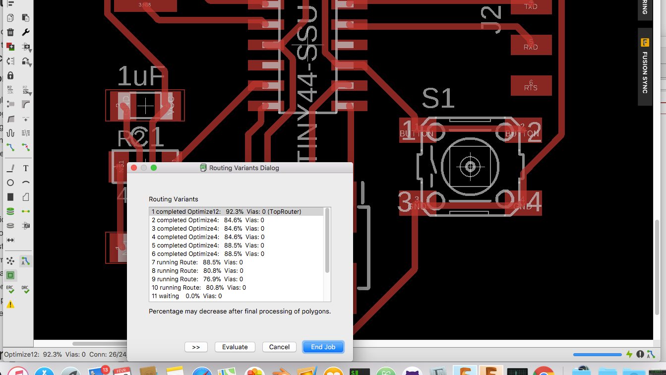
I was thinking for a while of a radical solution and now it was time to try it: erase all the files in the folder and start anew. So I erase all the files, which were many, contained in the folder. I reloaded a schematic that I done earlier and BANG!
100%
As simple as that: 100%
Didn't believed it.
The board is clean, looking sharp and different from the reference circuit. And it's my creation.
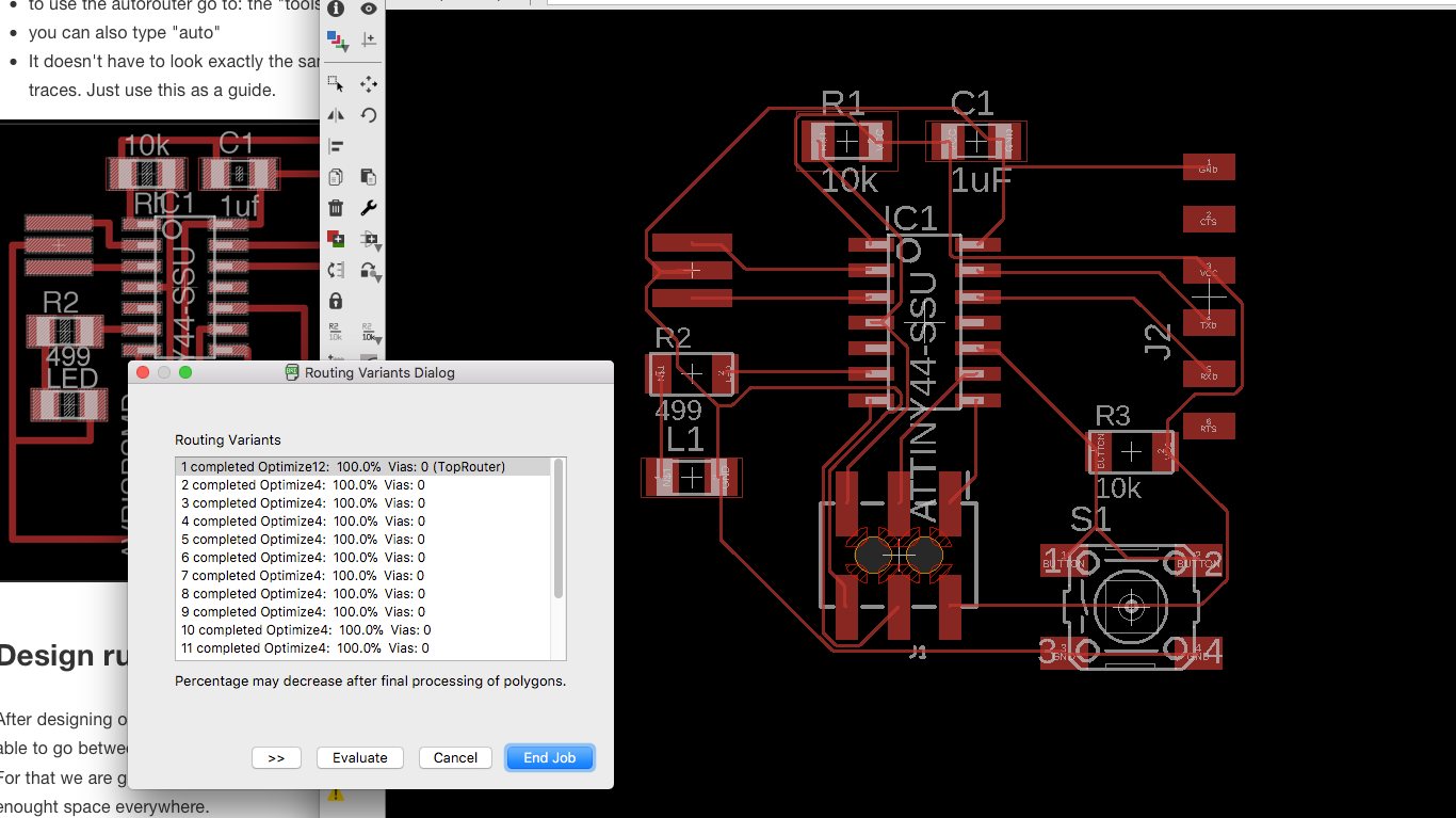
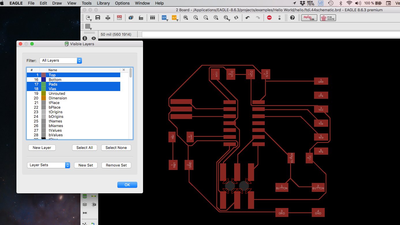
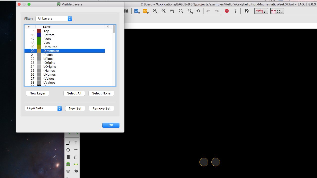
I followed the tutorial to prep the board. I was impressed with the board design. I exported the png file, added the white border and it's ready to be milled. I've also exported the dimension layer but I don't understand the result and will have to ask question about it on Monday.
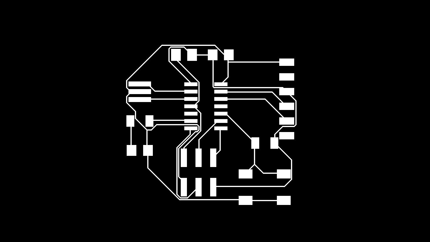
Prepping for milling
So the file is ready for milling. Before we do the actual work, we must go to http://fabmodules.org and upload the file to get the proper gcode for milling the traces. Under input format, we choose image (.png). I've learned that if this operation don't upload the file, you simply have to relaod the page and start again. You will get something like this:
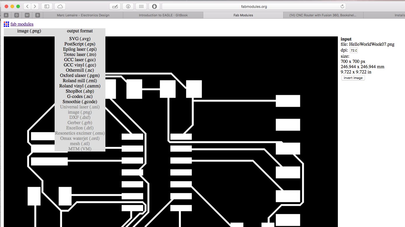
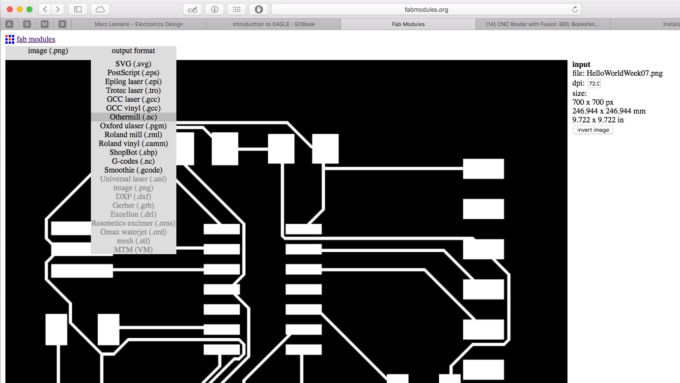
You then have to choose the output file format, the one that is machine readable. In this case, *.ngc (Othermill)
Then the process, in this case, the board will be milled for pcb traces at 1/64".
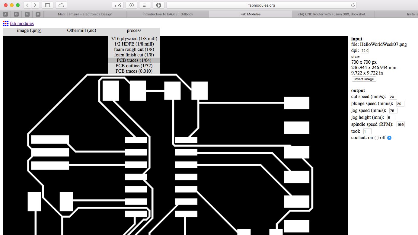
The last step before creating the file is to choose the right setting. We choose the default settings and see what we will get. Important to remember are the cut depth (0.1) and the number of offsets (4). Since our machine is a manual one, the rest of the options doesn't concern us. We press the calculate command to have the toolpath that the end mill will take. I save the file to a usb stick.
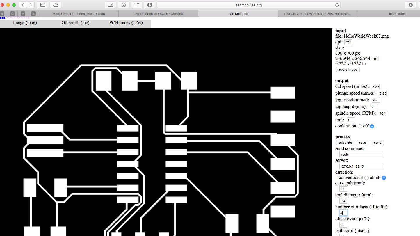
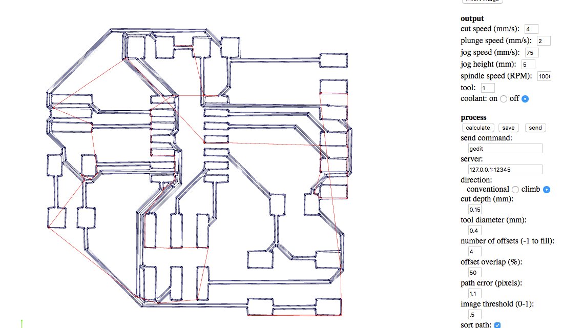
We made a first try with George's file that seems pretty much ok but upon inspection, the mill went too far and erased all the traces. Since he configured the cut depth at 0.1 and mine was at 0.15, it was obvious that I had to make some corrections.
Mathieu offered us two options, change the configuration or redo the file. I choose to change the configuration file with the mill going less in the pcb with a cut depth of 0.09, maintaining for the moment the numbers of offset at four, as per the recommendation of Neil, and hope for the best.
Being a Fab Academician is not easy
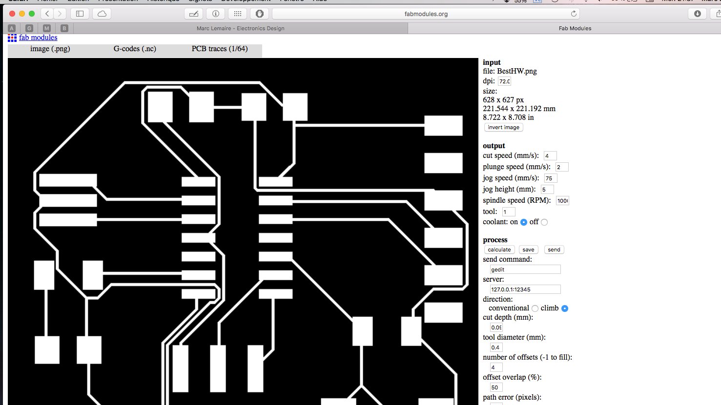
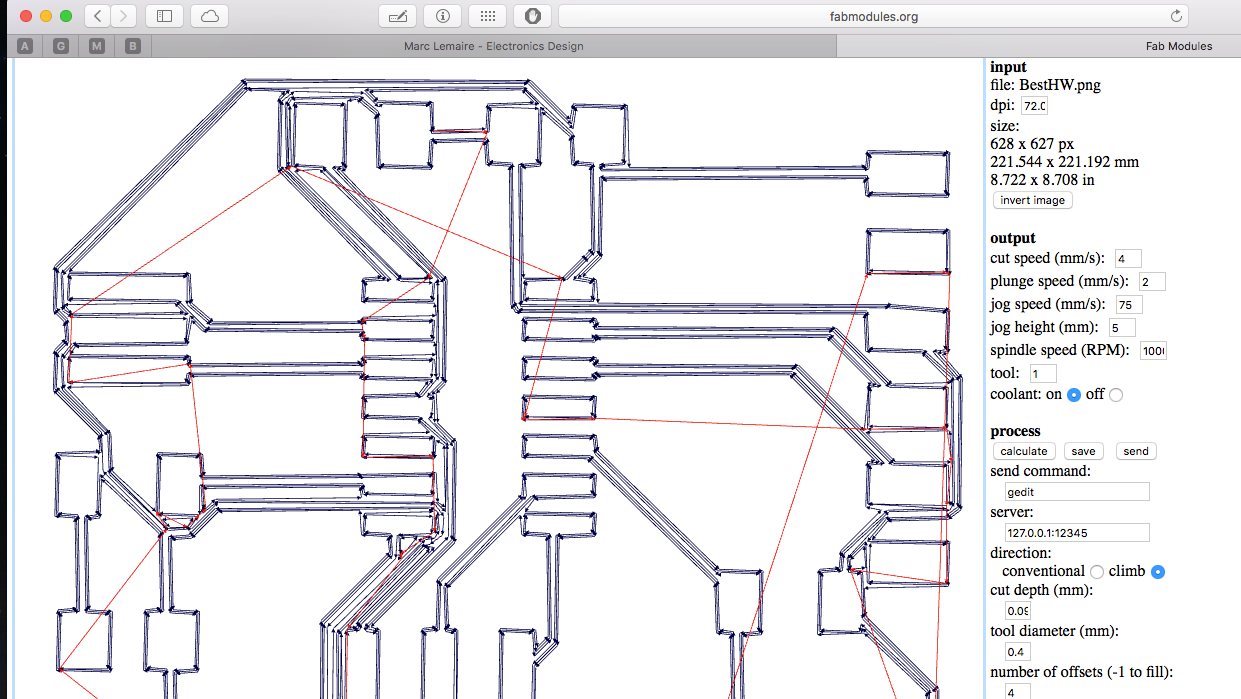
If you look carefully, there is a problem with the gcode file: it's about 8 ¾" by 8 ¾". It's waaay to big. I tried to locate the problem but it took me a week before finding a solution.
I submitted my problem to my mentor, Mathieu, and he suggested me to redo the sch file with a more appropriate symbol for the header pin J1 taken form the Fab library. So I changed the 6 pins header for this one: PINHD-2X3-SMD, redone the labels of the output pins and erased the old schematic. I went to the board view and placed the components near the lower left corner, like the reference image included in the tutorial. I pressed the autorouter button and the board was correctly generated on the first try. Almost too easy. But it also proof that I've learned much in such a short time.

The initial output had some issues with the traces, which were too thin. A quick correction within the Design Rule Check (DRC) where I incresed the clearance from 6 to 16 mils. Also, never forget to apply those changes...
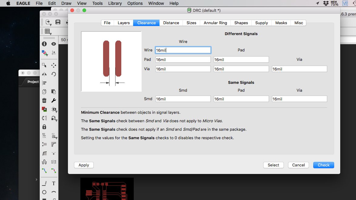
I exported the monochromed image with a resulution of 500 dpi and took it with my photo editor (Pixelmator). I only had to crop a little and it was ready for Fab Modules. I uploaded the file, chose the Othermill for g-code output format, followed by 1/64 PCB traces for process.
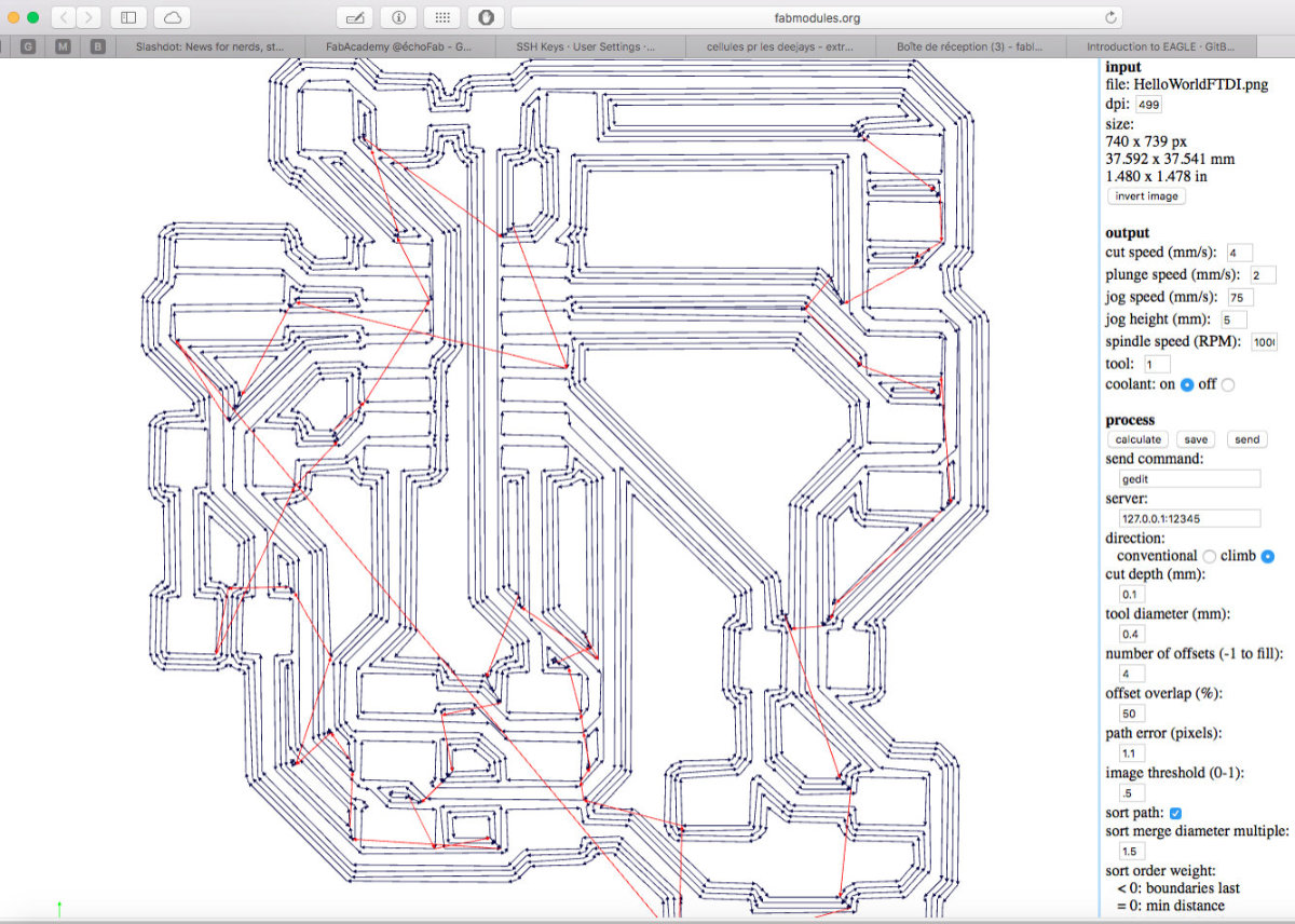
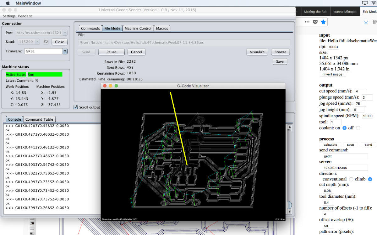
I changed the cut speed to 4mm/sec, the plunge speed to 2mm/sec, left the cut depth to 0.15 and the number of offset to 4 as Neil strongly advised. I press the calculate button, inspected the file (now it was really nice and I had the correct dimensions of about1 1½"x1½") and was ready to go to the mill. Before going to the machine, Mathieu suggested to download and install the software Universal Gcode Sender on my computer so that I will be able to use my computer instead of using the lab's. I thought that it was an excellent idea and made the install. After that I went to the shop.
This Dragon isn't so terrible after all
Although I had previous experience a long time ago with a machine that was industrial grade and mastered the g-code that controled it, I was not comfortable with this small machine. It took me the appropriate environment to really familiarize myself with it and the software. I connected the arduino to my computer, selected the baud rate (maximum at 115200) and press the open button. I then zeroed in the head with the X, the Y and the Z axis using the machine control tab. I placed the Z axis at zero with a piece of paper, resetted all the axis and moved up and away the head and made a "Return to zero" test. Everything was fine. So I sended the send command from the "File Mode" tab.
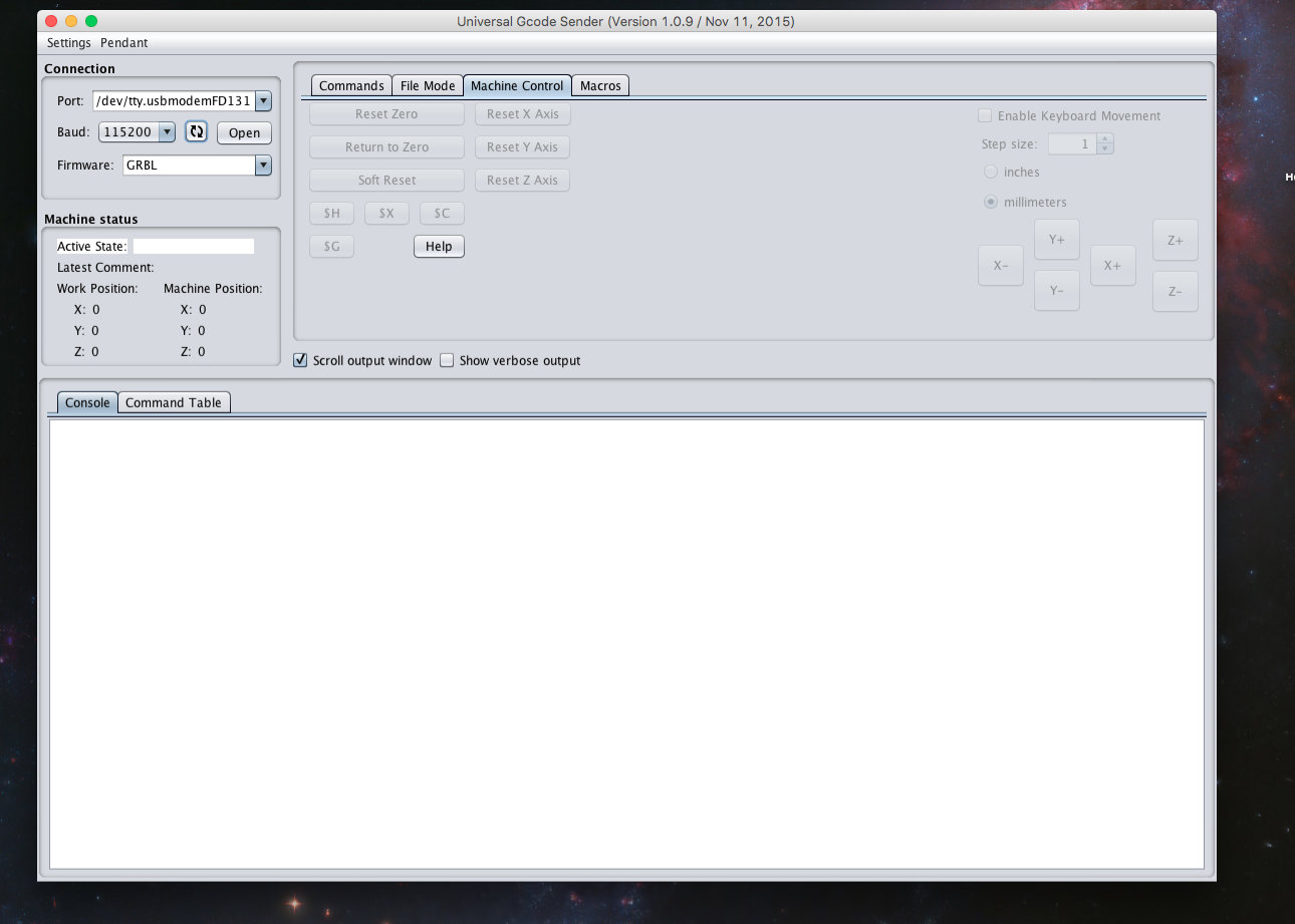
And the head went up and away from the plate.
I was puzzled. Although I was careful, this behavior was not what I expected. I ressetted the machine just in case. I logged out of the computer, rebooted and started the software again.
The head went up again!
I called for help to chack if I've done something wrong but was ok. We tried three times with the same results.
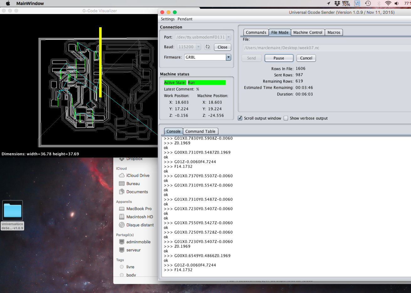
Something was fishy and we were now trying to find a solution. Mathieu tested the machine with a file of his own and it went fine. So somewhere, there was a bug in my file, lucky me. He used his computer to make a config file from my file. I transfered the file to my computer and went to the shop. I started the mill and to my relief, it was finally doing it's job. But it took most of the afternnoon to get to that point. And I still wasn't sure of the end result.
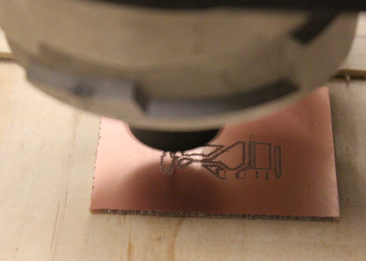
After 11 minutes, the mill came up and I had my Hello World pcb. At last! The traces are good but a little shallow. I checked the traces with a VOM to make sure that there were no shorts. They were two or three but I fixed them by cutting the contact with an X-Acto. I doubled checked the circuit again and it was ok. Since I had some time left, I tried to make another board but the plate was not level, making uneven traces.
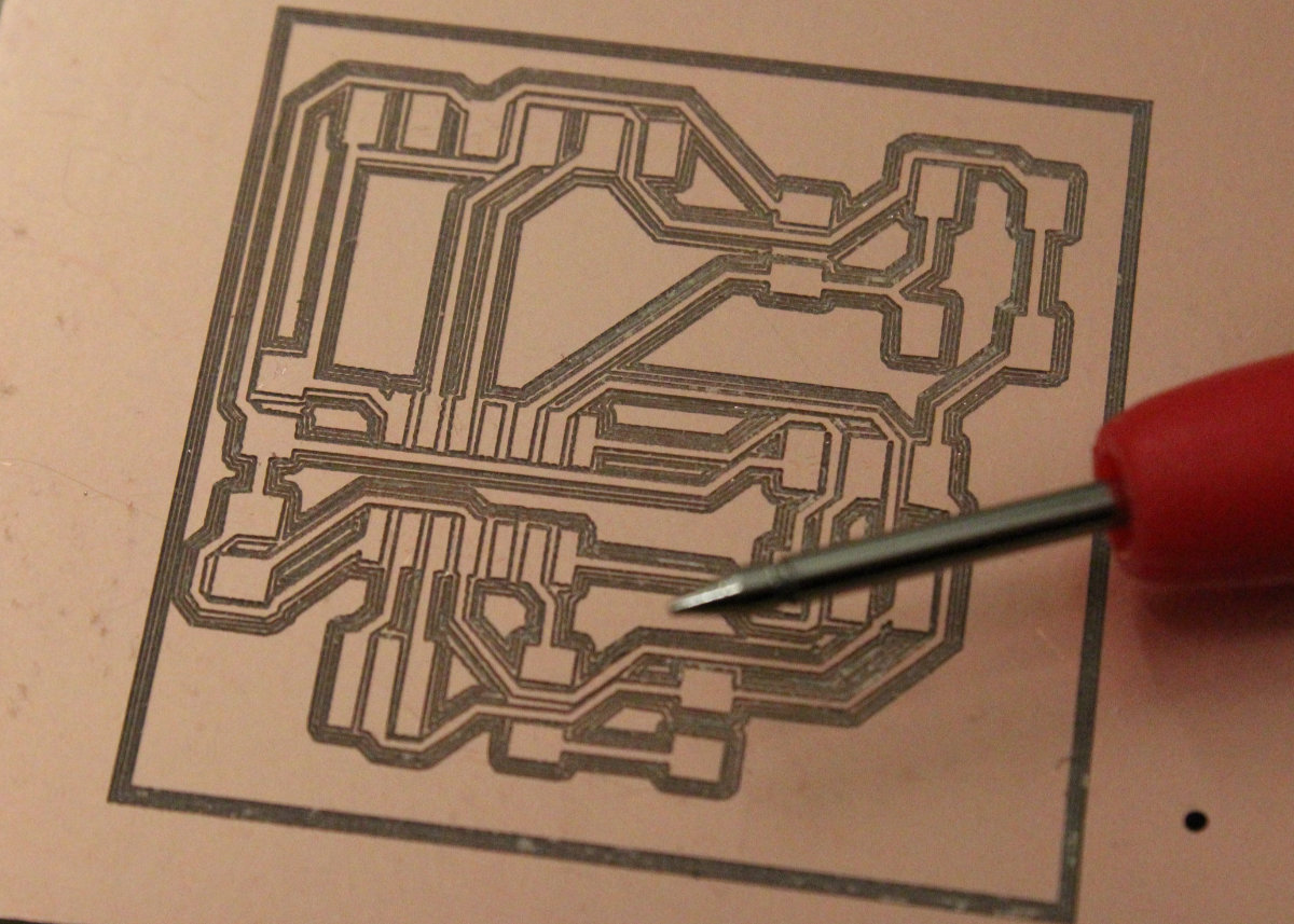
And now I finally completed my printed circuit board. Next will be the soldering of the components.
Learning is hard
Next Wednesday came and I was prepared for the next step which consist to solder the components to my board. After lunch, I prepared the tools and searched the components to be soldered, but I immediately faced a few problems. First, I stressed a little lost my steady hand. As I tried to compounded it, it became worse. I wasn't comfortable enough, the tip of the iron was not appropriate for such a delicate job. I had some issues with the temperature of the soldering iron, which was too low, and the solder stayed on the tip instead of flowing gracefully to the soldering pads. I started out at 375°C and incresed it until I reached 425° but I still have issues. Maybe it's the solder, a no-lead type that is more difficult to use. Desperate, I picked up an available iron with a finer tip and started to do some actual work. I was proceeding well until I put too much solder on the board when I tried to solder the crystal. I immediately knew that I made a bad move as I was unable to solder the crystal onto the board, the crystal body acting as a heat sink and not letting the solder melt. It became evident that I must remove the excess solder with a soldering wick, which I never used before. I started out ok, but by trying to be too perfect, the copper trace came away with the wick. The board was scrapped. Maybe it is for the best as I'm not proud of the connections that I made.
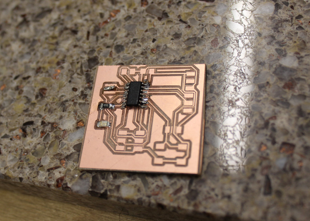
Bad move.
It was late in the afternoon and decided that if I couldn't continue with soldering, at least I could make some circuit boards for the next session. I had about 45 minutes left before the lab closed. During that time I managed to place a board, make the setup, zeroed in the origin, make the return to zero and start the milling. Although at first glance it was nice, I milled too deep. I quickly put another plate, redo the setup but started with a slightly higher Z coordinate. But it was too high, the mill was a micron over the surface and wasn't milling anything. I stopped, went back to the setup, corrected the Z axis and started again. At first it looked ok but I suspected that I was milling at the same depth. It was too late anyway and left the program run it's course. Once done, upon visual inspection I was skeptic that it was ok. I tested the traces with a VOMeter and was surprised to see that some traces that looked no go were in fact go. But I found some that weren't conducive at all. I checked the other board and found a similar problem. So everything that I've done today was for naught.
A sad end to a very long day.
Investing in good tools is always the best option
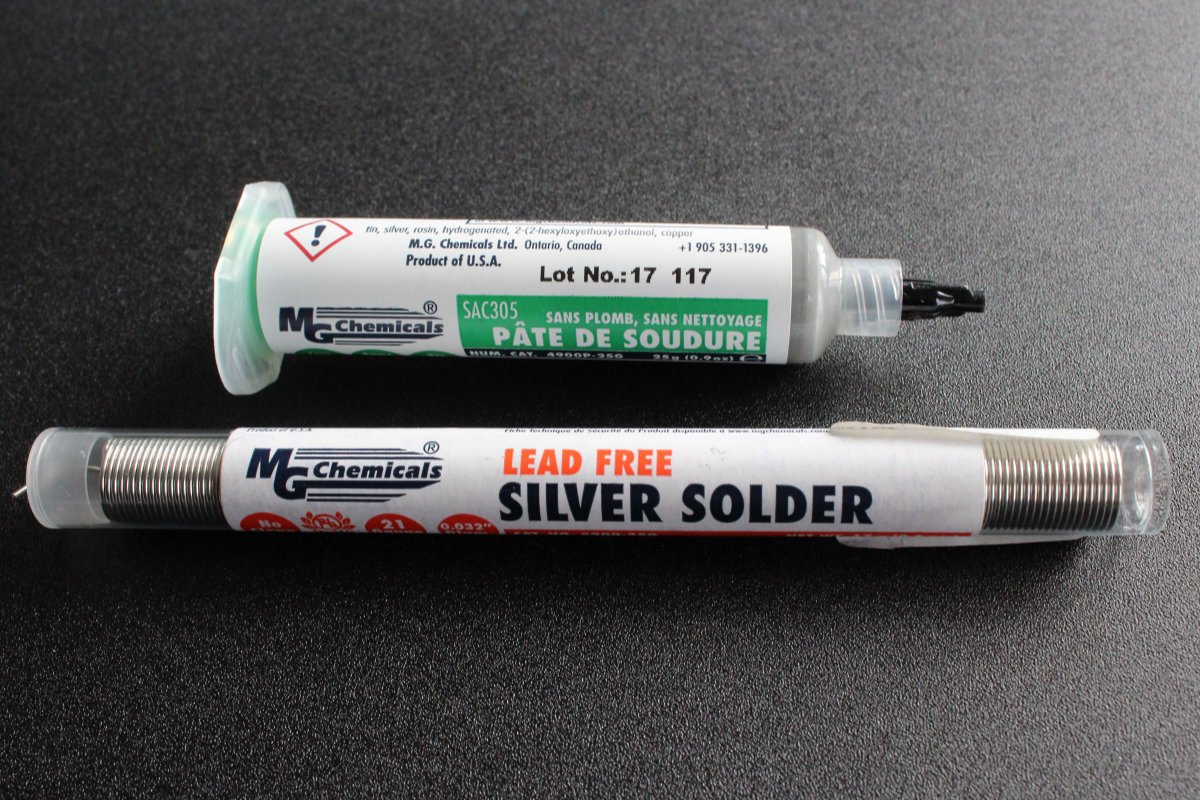
At the end of my last session I was so frustrated of my very poor performance that on my way home I stopped at an electronics shop and bought some supplies. First I chose a very fine tip for the soldering iron. Second, I picked up a soldering paste in syringe and the appropriate solder that goes with it. I was at a loss in the store as to which one to choose and decided on the Sn63/Pb37 mixture. I just made a search and it seems like a good choice. It is a mixture of hight purity alloy composed of 63% tin and 37% lead. It a low drossing, high wetting solder that has a melting point of 183°C.
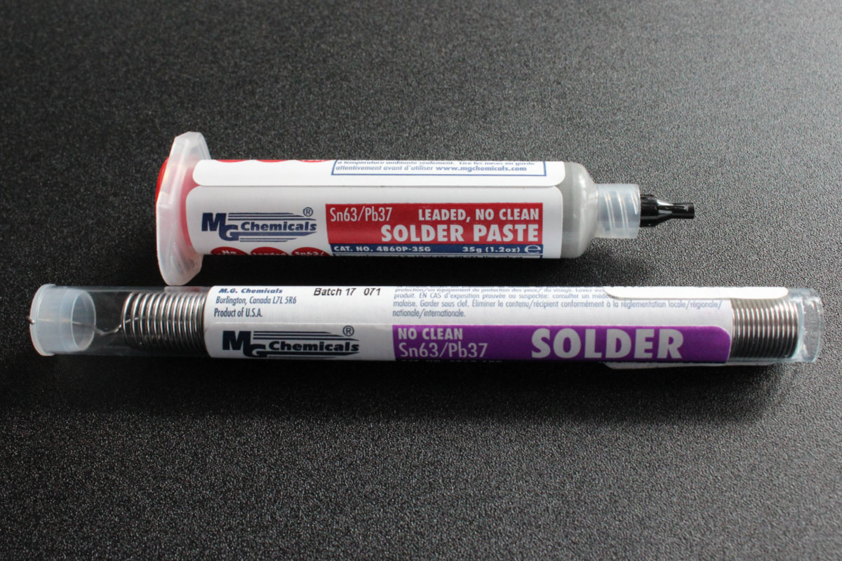
I manage to made a few pcbs one morning: one too shallow, one perfect but my new computer went to sleep mode, **expletives deleted**. I finally made two other good boards. I then prepered my soldering station and was ready to solder around noon.
What I experienced today was more in common with was I'm used to when I solder. Only this time with more precision. I started out setting my soldering station at 375°C but soon found that the solder wasn't flowing enough. I incresed the temperature to 385°C and immediately obtained better results. The soldering points are good and nice but I need to practice more. The chip was installed relatively fast and easy. The rest were put in place with no problem at all except for the crystal, where I made the same mistake as last week but manage to work my way out of trouble. I stopped only because there was one part missing that is on order. I will be able to finish the board this week and start programming.
When you discover the toxicity of one mundane metal
I was pround of what I've just bought but the day after came out a new study by The Lancet Public Health Journal. The study has an appropriate title: Lead and the heart: an ancient metal's contribution to modern disease. An enlightening except:
A key conclusion to be drawn from this analysis is that lead has a much greater effect on cardiovascular mortality than previously recognised. Lanphear and colleagues' calculation that lead accounts for more than 400 000 deaths annually in the USA represents a tenfold increase over the number of deaths currently ascribed to lead. The authors argue that previous estimates have produced lower numbers because those analyses assumed that lead has no effect on mortality at amounts of lead in blood below 5 μg/dL and, thus, did not consider the effects of lower exposures.
So what I just bought was now really dangerous not only for my health but also for all the people around me. Now, there is two choices left to me to: buy a lead free alloy or go silver: I chose the latter because the solder joints are of a higher quality.
Taking the Silver route
Next morning I was back at the lab ready for action. I've heard that soldering with silver is difficult and need more higher temperature. I metered my station at 300°C but rapidly increased the temperature to 310°C with testing by touching the hot tip with the solder. Once the temperature was corrected, I found that the silver melted rapidly around the joint, leaving a nice shiny surface that I'm sure is conducive. I made just a few solder points, the last six for the Hello Board, but those points were perfect. It must be noted that I added to my toolkit a set of soldering tweezers, including one with reverse action. This one was the main reason why I picked up this kit and it proved to be a good investment on it's first use. On my next visit, I found a lead-free flux paste and a flux cleaner to get nice clean boards. But you must read the instructions because it's recommended NOT to have skin contact with the liquid. So, ALWAYS wear gloves when using this product.
Looking for trouble
One problem has been taken care of, but there's still another one to fix. I noticed something odd while working with Eagle: when I export the monochrome image at 500dpi, as recommended in the tutorial, the dimensions are doubled when imported in Fab Modules. I noticed this problem when I was working with George while doing our boards. We tried many hacks to no avail but eventually, I transfered the resulting png file from my computer (MacOs X) to George's (Win). Suddenly, the file was at the correct dimensions. I send a message to my regional mentor asking about this stange behavior and he told me that there this was a known bug. What's more puzzling is that my mentor, Mathieu, has a Mac and never had this problem.
In case of doubt...
Within my application folder, I had three versions of Eagle and many iterations of the Hello Board. Having too many test files is not a good thing as this lead to confusion. I started to wondered that maybe starting (almost) from scratch will fix the problem, or at least locate it. And if it doesn't work, I will have a clean board and located a bug. So I erased everything, made a clean install of the latest version of Eagle (8.7.1) and place my precious schematic file in the eagle folder. I quickly redo the board plus adding a plus and minus sign to my schematic so as not to repeat my mistake again, and export the png file to my desktop.
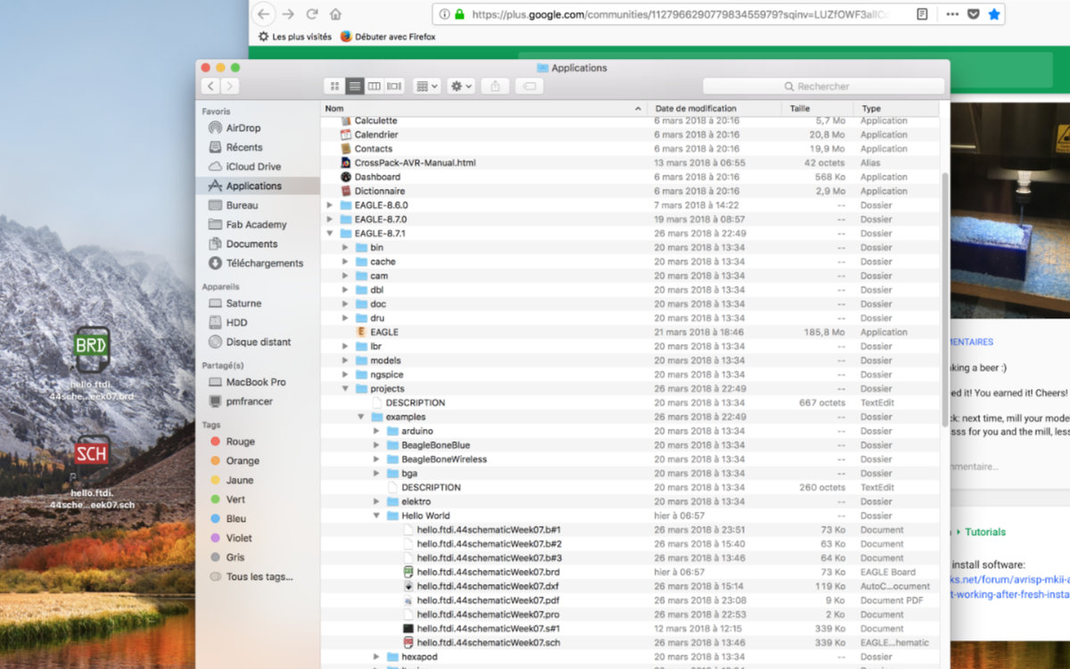
The bug is still there.
The final solution
One solution that I did find was exporting the image from Eagle in the recommended dpi settings (500) and then doubling the dpi in Fab Modules (1000).
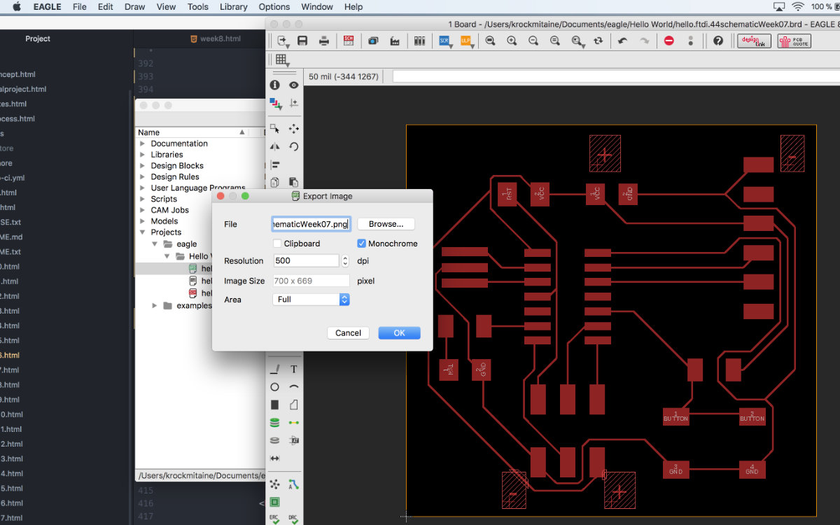
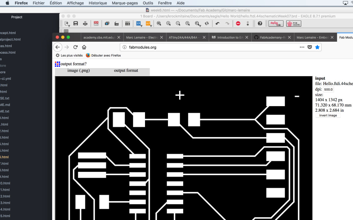
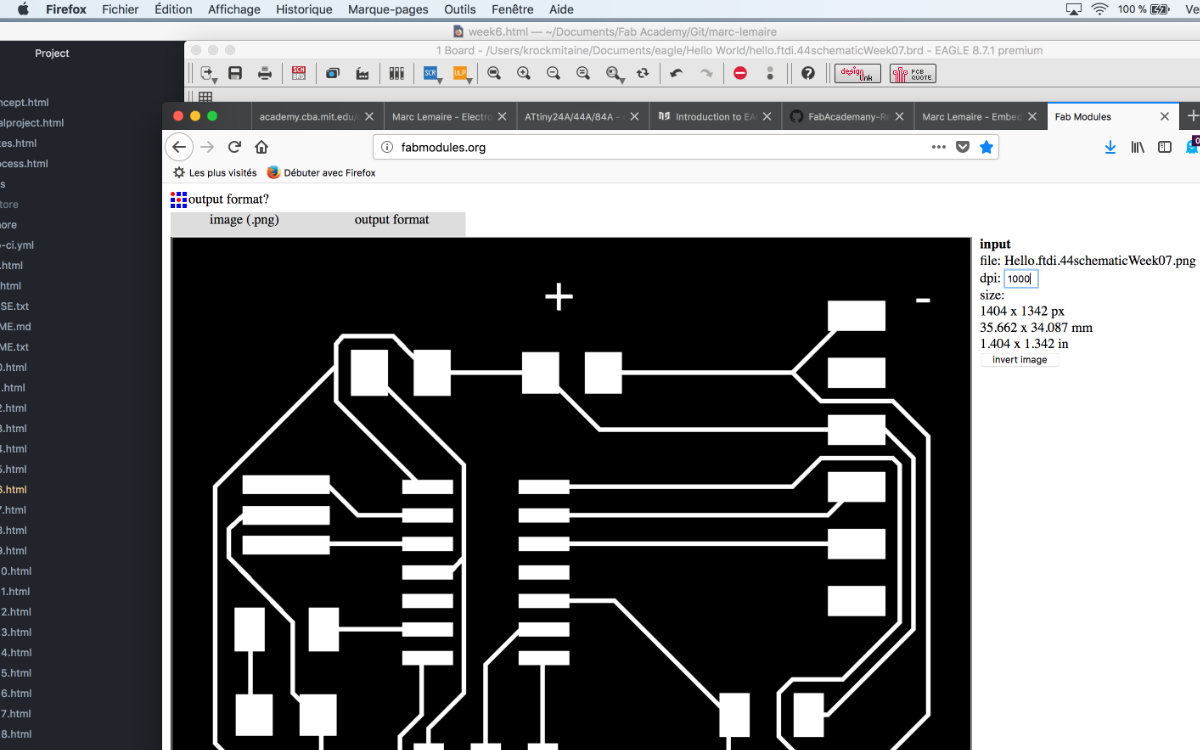
It only remains to make that file again and verify that everything is back to normal.
The final test
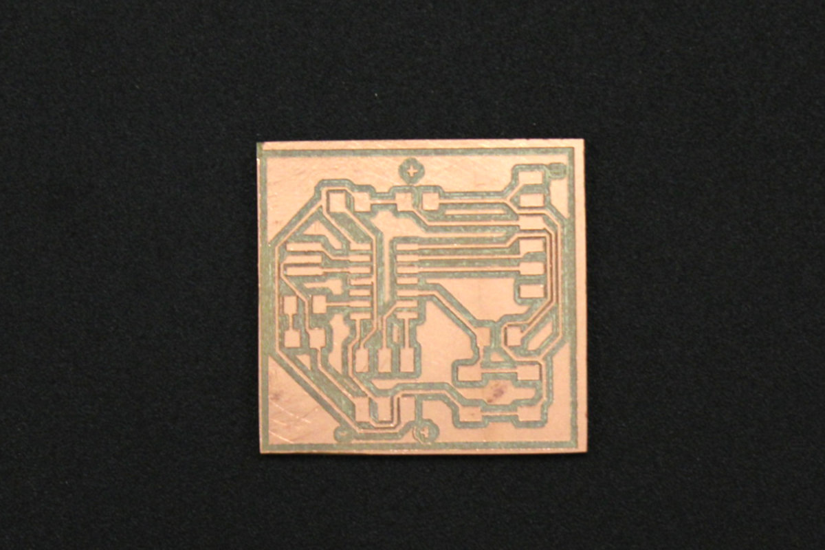
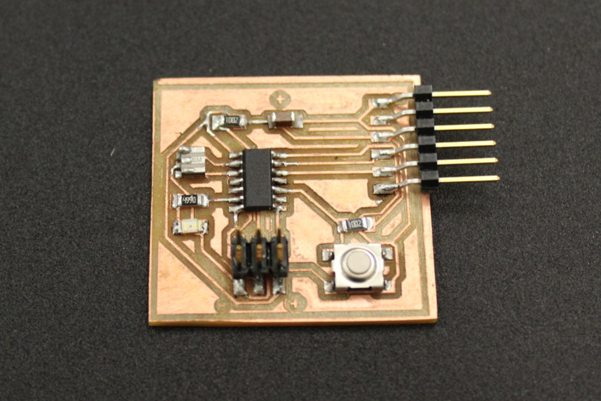
I was finally able to make my board and everything went according to plan, which is an unexpected outcome for me. The first board was not beautiful as I went too deep but on the second try, I configured the mill to go to 0.08mm. I was uneasy at first when I pulled out the board from the plate as there was much burring left over, but after some delicate sanding, the burrs were gone and had a pcb with nice traces.
One last remaining task and I'm done
Now that I define a bug and not that many people seems to be aware of, I need to warn the software maker of this problem and describe my system and the process that I've used to help them squash this bug.
Not so fast!
I thought that I was done with this task but there's still the board and the testing part that needs to be done. I went to Alec's lab to make my mold but I ended up making the board instead. On Monday at échoFab Mathieu wanted to make make a new board from scratch because nobody had a functionnal one. So we fired up Eagle and made the Hello Board from scratch using the Fab library of components. I was actually surprised at how fast we made the board. Once done, I went to the shop and milled the board. After lunch, I soldered the parts. Now I realise that I made a design, milled and soldered it in a day. Not bad! I think I'm getting up to speed with electronics production.
Once everything was done, Mathieu connected the board to his computer and the light went on as expected.
But upon uploading the code, the arduino ide stopped with the message that it can't upload. I tried to locate the problem with one fully functionnal board but I can't locate it.
Later on, Mathieu found out that there was a bug in the schematic that we've done. Although we were two, and double ckecked the schematic, there was one path that we missed and that was the reason the board wasn't functionning.
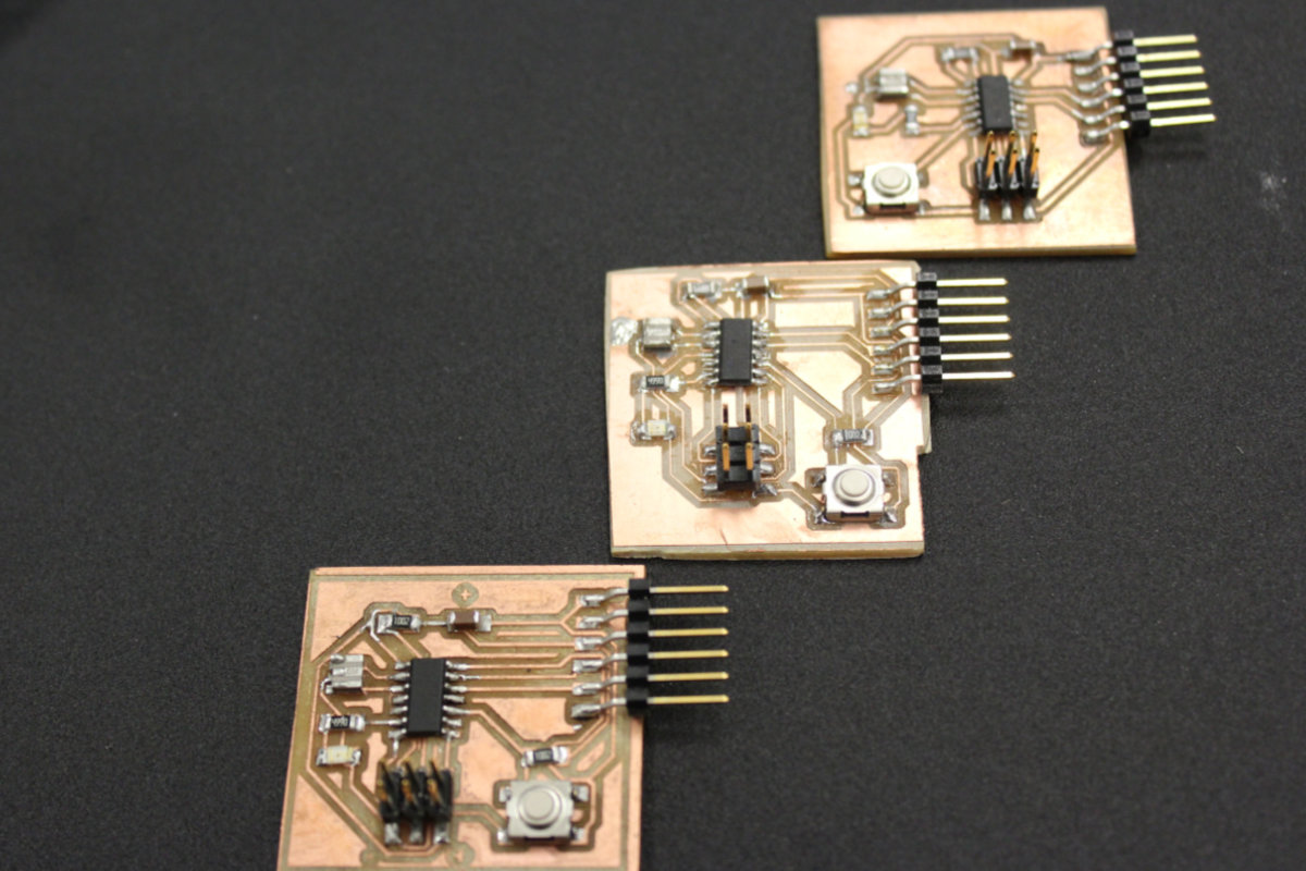
So back to the milling machine and I made another board and soldered the components. But somehow, all those boards were non-functionnal. My tutor then told me it was time to move on and come back later. I had no other choice but moving along hoping that this will not come to haunt me.
Another try, and fail...
By now, after a fouth attempt it's becoming a pretty boring story, and not a particularly entertaining one for me. We had so many difficultiers making one board that our instructor made a functionning sketch. By now, the milling machine is working fine. George made four circuits of the Hello Board at the same time! One day we met and made our board together. I was particularly optimist about the outcome as the board and schematics were tested. I made my board, taking care that my soldering was nice, that the led orientation was correct. I had a tough call concerning the external clock as the traces are narrower than the part. Being too close, I had to cut with a knife some copper otherwise the resonator was grounded. While cutting, I pulled off some copper from a trace and I had to improvise to make a jumper cable. Tough call but I made it. After soldering the chip and the resonator, the rest of the components did not represented any challenge and were soldered to their respective places.
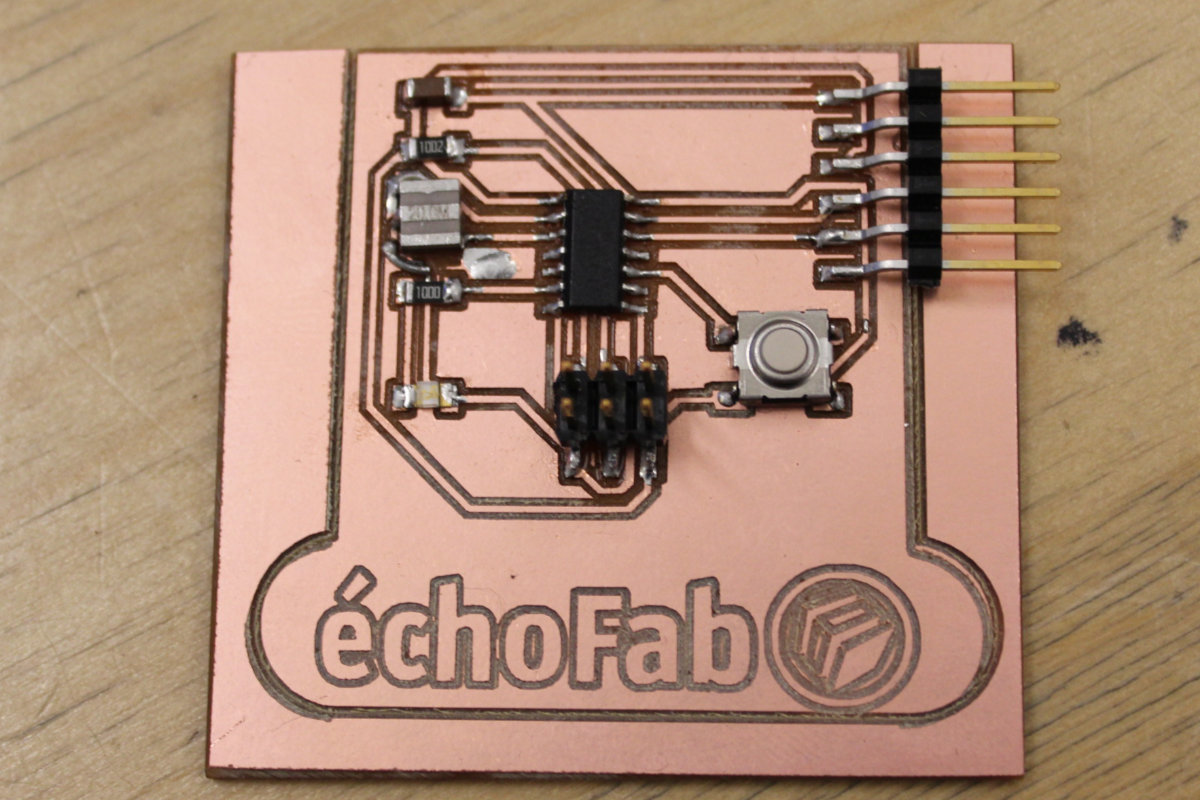
When you have this sinking feeling that something is not right
So the board was done. Now it was the time to connect and push the code to the ATtiny. The connections were done with the FabISP and a FTDI cable. For once, the Arduino IDE didn't made me miserable and I was able to push the code.
Concerning the code, I used the Mathieu's code. I verified my schematic against his and modified it for my setup, which was setting the buttonPin and the ledPin.
// set pin numbers:
const int buttonPin = 10;     // the number of the pushbutton pin
const int ledPin =  6;      // the number of the LED pin
// variables will change:
int buttonState = 0;         // variable for reading the pushbutton status
bool led_on;
void setup() {
  // initialize the LED pin as an output:
  pinMode(ledPin, OUTPUT);
  // initialize the pushbutton pin as an input:
  pinMode(buttonPin, INPUT);
  led_on = true;
}
void loop() {
  // read the state of the pushbutton value:
  buttonState = digitalRead(buttonPin);
  // check if the pushbutton is pressed.
  // if it is, the buttonState is HIGH:
  if (buttonState == HIGH) {
    // turn LED on:
    digitalWrite(ledPin, HIGH);
  }
  else {
    // turn LED on and off:
    if (led_on) {
      digitalWrite(ledPin, LOW);
      led_on = false;
      delay(50);
    } else {
      digitalWrite(ledPin, HIGH);
      led_on = true;
      delay(50);
    }
  }
}
The verification process went really fine. To my surprise, the uploading process went as it supposed to do. I saw the led light turned on, but I immediately knew that something was wrong. The light the led gave off wasn't bright blue but a sickly blue light, as if I had put a 500 ohm resistance, which it wasn't (100ohm). I press the button to see the actuaction of the code, but the feeble light gave out and the led died right there. I was so quick I never had the time to think about taking a picture.
So I guess it's back to square one for me. But at least there's a silver shinning: Goerge's board is working perfectly. We worked together, put the same components on the same board, helping each other out and giving tips. He manage to program his board and make it do the programming. As we compared our technique, the only thing that differentiate our process is that I used flux. My hypothesis is that the melted flux has made connections between traces, once the electricity was feeded in, the board litterally shorted itself out. For the next, and hopefully last, board I will not use the flux paste.
Follow the guide!
Go read the follow up on this assignment, Programming the board, in the Embedded Programming week
