Electronics Production
Week 5
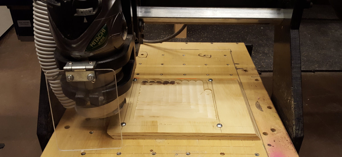
We started this week assignement with high hopes. With this week presentation, I learned new ways to produce PCBs. Having done some decades ago when I was young, with chemicals and pen tracing, it was a messy and, I found out, polluting. We now produce PCBs with a milling machine, bypassing the breadboard step. Having done some at BennyFab, I was never satisfied with this method of prototyping as I discovered that when you do breadboard, you must always be careful when you connect the components to the breadboard with the flimsy wires and connectors. A slight mouvement and you can lost a connection and have to hunt down the location of the problem.
As it is a group assignement, we decided early on to settle on one model of the programmer and produced as many units as possible, taking into account that we will lost some during the soldering process. We had an introduction course on how to use the machine and it's many peculiarities. This machine has a DIY pedigree, and it shows. The connection between the computer and the mill is via an Arduino that transform the digital signal to the RS-232 serial cable.
We also learned that we have to prepare as many small boards as possible because the machine can't make many boards at once. We could take the chance but if we don't succeed, we lost the entire plate.
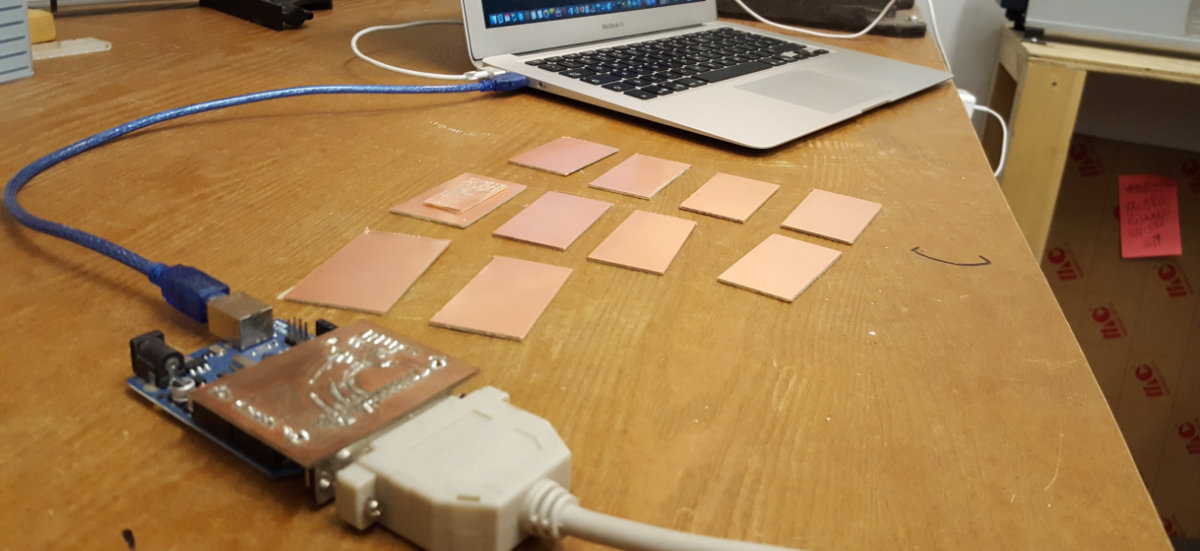
Software and hardware have limitations. No end stops security, almost none for the humans around (only the plexiglass in front of the spindle). If the connection is lost with the computer, the machine stops and you lost your production.
Not good.
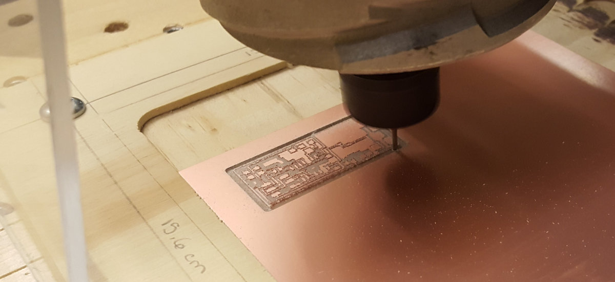
After these many warnings, we prepared the machine and tried to make a PCB. The first result did looked good from afar: we had pathways, but had Z axis problem (too deep) and some burring issues. Upon close inspection, we saw that the pathways were wiggly. We had to remove the first sample for inspection and keep it for our reference.
The second attempt wasn't successful at all: the plate was not level and one side of the PCB still had some copper left, making bridges between pathways. I was really concerned that we couldn't produce our PCB in a consistent manner. We called it a day on this sour note.
The next day
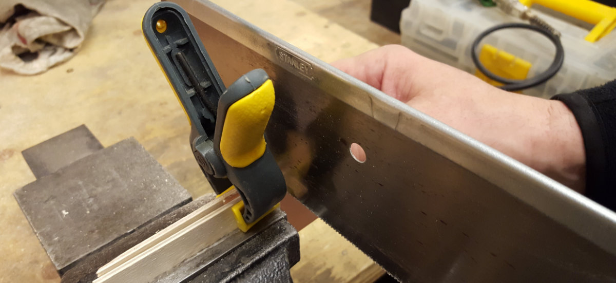
Next morning, with the help of Geoffroi we decided to prepare small plates for each programmer. After a small search in the shop room, and reaching for two small scraps of wood, I made a sandwich of two pieces of wood and used a mitter saw to cut a copper plate into smaller elements.
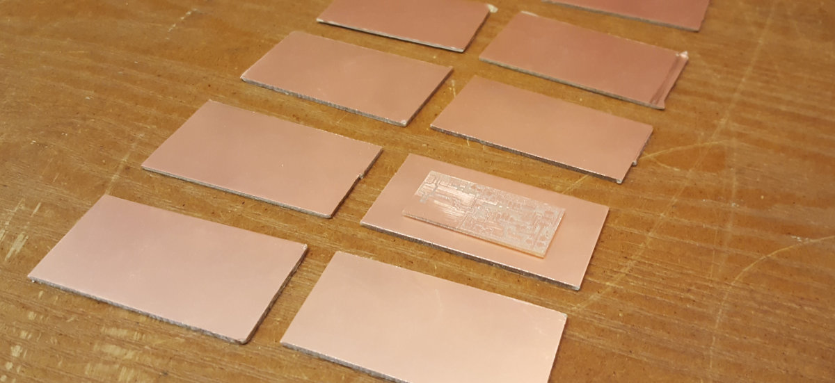
We were now ready to make our own PCB. We prepared the machine, configured the software and started the machine. By this time, George was there as well. We setted up correctly the reference point and started the program. The milling machine went into action without a problem, so by itself it was a small victory. But we didn't produced a satisfactory sample. More trials and always the same problems surfaced: too deep, pathways not connecting. Or almost not. Burring issues. We had to check each of our production and became bogged down with the configuration of the milling machine instead of producing our samples.
We were able to produce one item that, upon inspection, didn't looked good but all it's circuits was ok. The problem was that the next one, with the same configuration produced a different result.
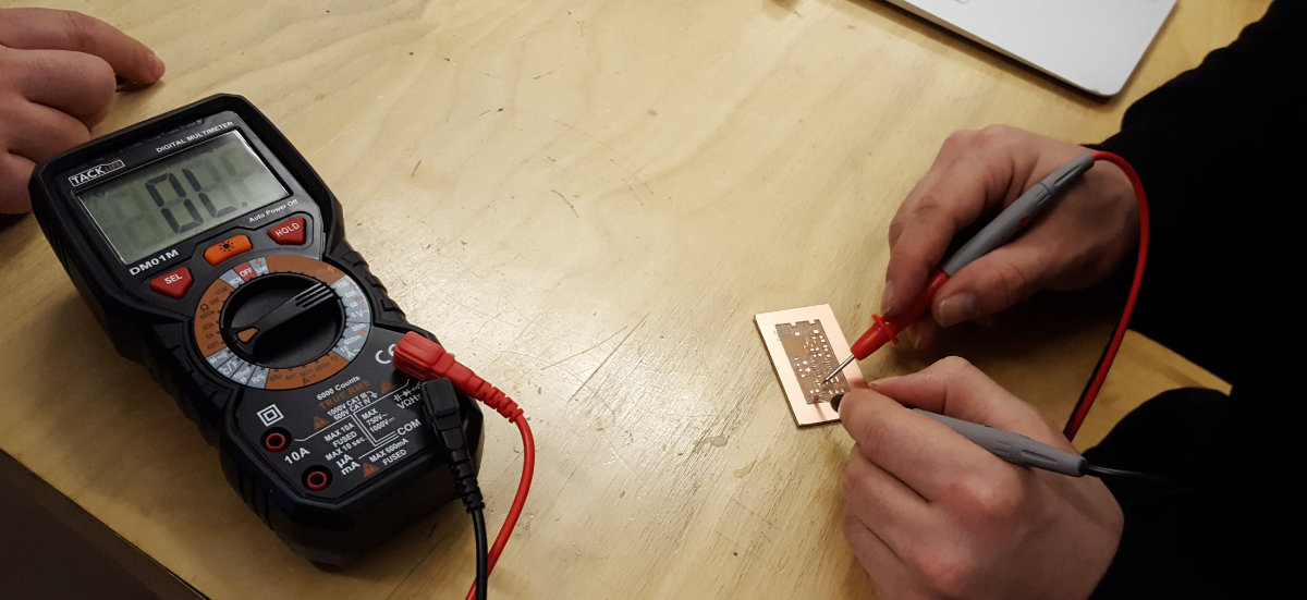
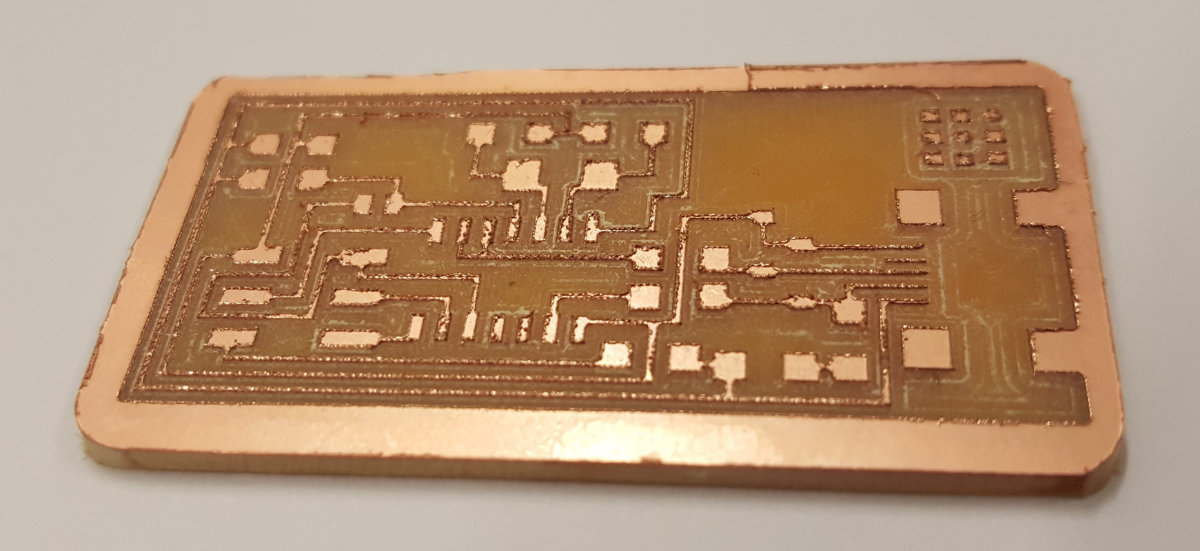
Eventually, Mathieu came up with an elegant solution. Since the machine is not precise and can't make repeatable results, we will change our board model to a larger one with generous pathways and less stringent tolerances that will be more easy to produce.
Let's get physical
On Monday, I came with a nice surprise: the boards were made by Mathieu because the machine didn't performed as expected last Thursday. Mathieu's investigated our problem and after investigating the problem, he located the problem and he told us that we were almost on it, but not quite.
So, I had a pcb, parts and a soldering iron. It's not my first time that I'm using a soldering iron. But I've never done with so many tiny parts. Also, I have a physical weakness: I do not have a steady hand. Never had unless I became zen-like. Since I only had one board, I didn't want to destroy it by accident and lost precious time.
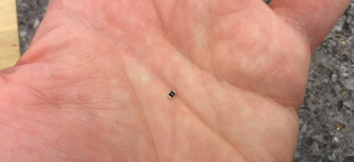
Analysing the board, I came to the conclusion that I had to start with the toughest of all: making the contacts of the mini-usb connector. I made myself comfortable with my surroundings and learned new ways of doing solder. Like nowadays, flux solder are sold in syringe, less messy and more precise than the traditionnal tin can. You solder directly to the pcb: you no longer have to drill holes and cut wires on the other side once you've done (I hold this idea on the same level as sliced bread). Use a stone as a safe surface for your solder. And you can use glue to hold these tiny parts in place before applying solder.
When ready, I started to solder my port. It's really difficult to solder at this tiny and it's a challenge to my soldering skill. But on the first pass, I solder those channels and after inspection with a volt-ohm meter, I declared them ok!
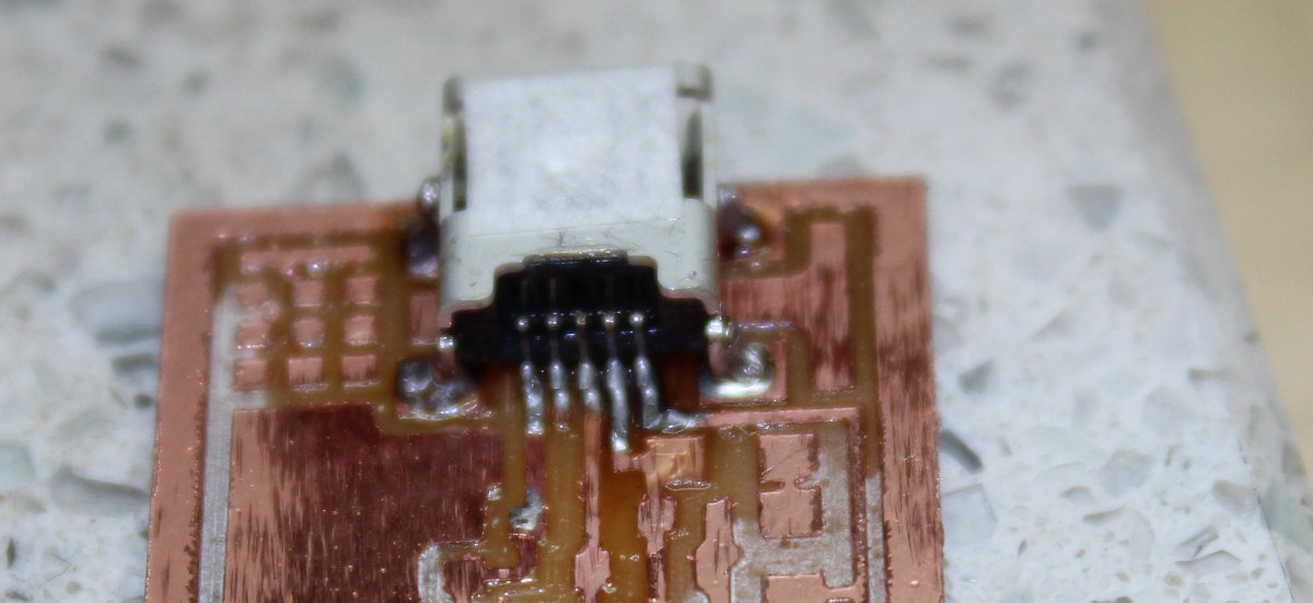
Once this task done, I next soldered the programmer in place. With the help of the pcb scematic, I tested the connectivity of all the connection and they all passed.
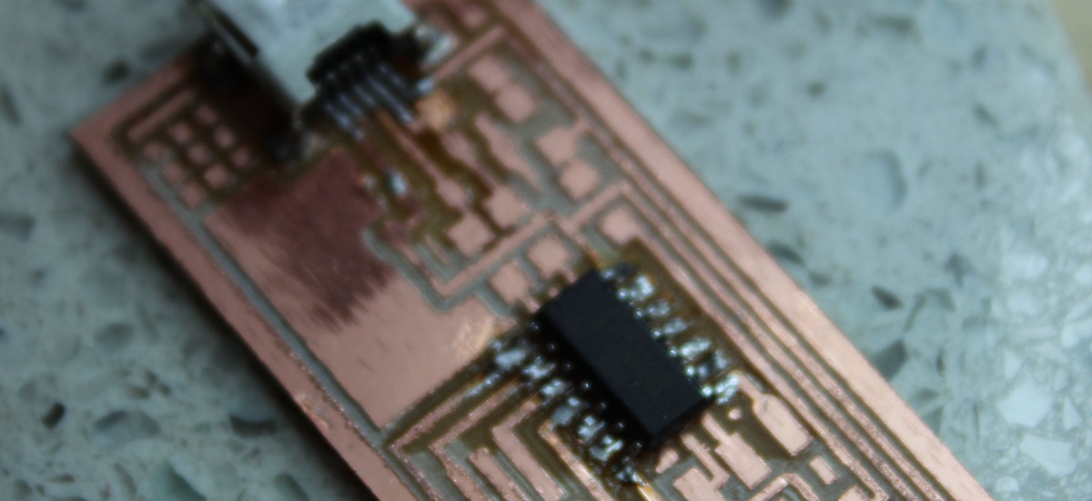
I then started to solder a resistances then realised that I had to make a scenario for the soldering sequence. So I started to make my way starting from the mini-usb toward the front. I was careful about the placement of the diode: the real tiny line indicates a negative, or cathode and must be place according to the plan. Each time a diode or a resistance were soldered, the connection was checked with the VOM meter.
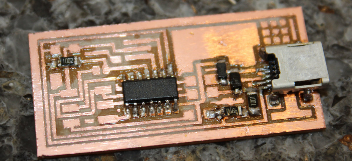
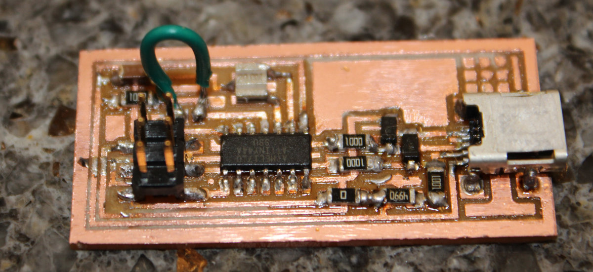
Slowly, I made my chip. The jumper was done but wasn't happy with the way it looked.
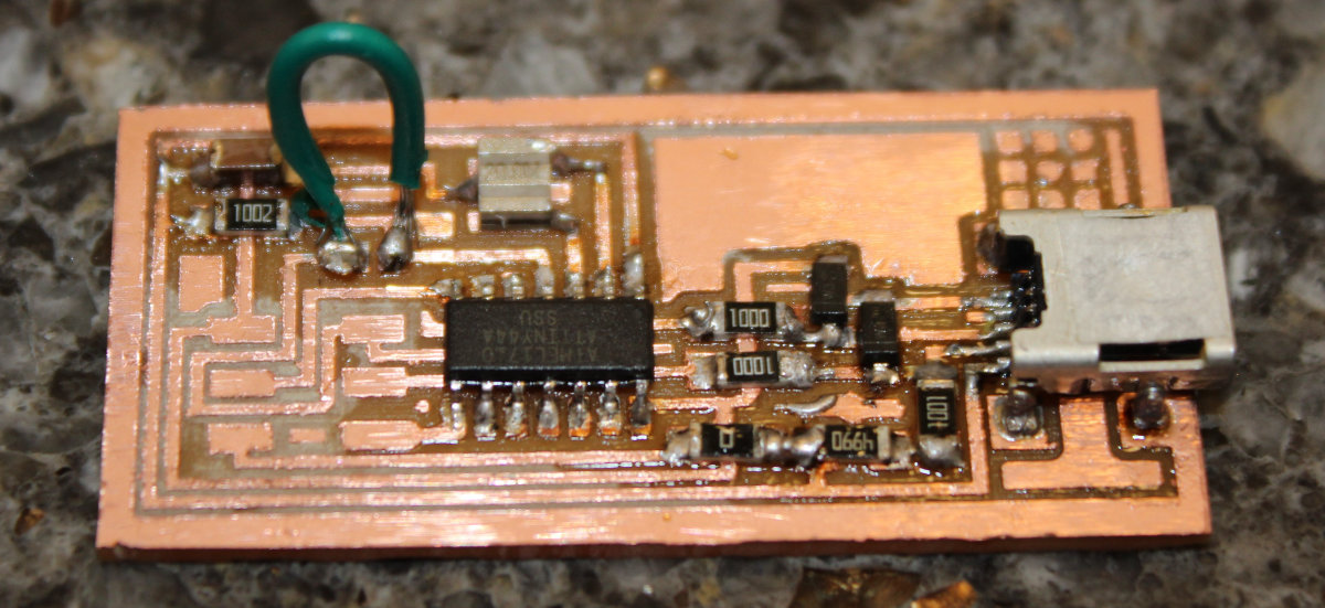
Finally, the connector was done and my programmer board was complete, but untested.
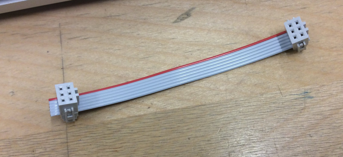
One last component needed by the programmer is a cable connector. I cut a small lenght of ribbon cable and press fit the connectors, being careful to assemble them with the same orientation.
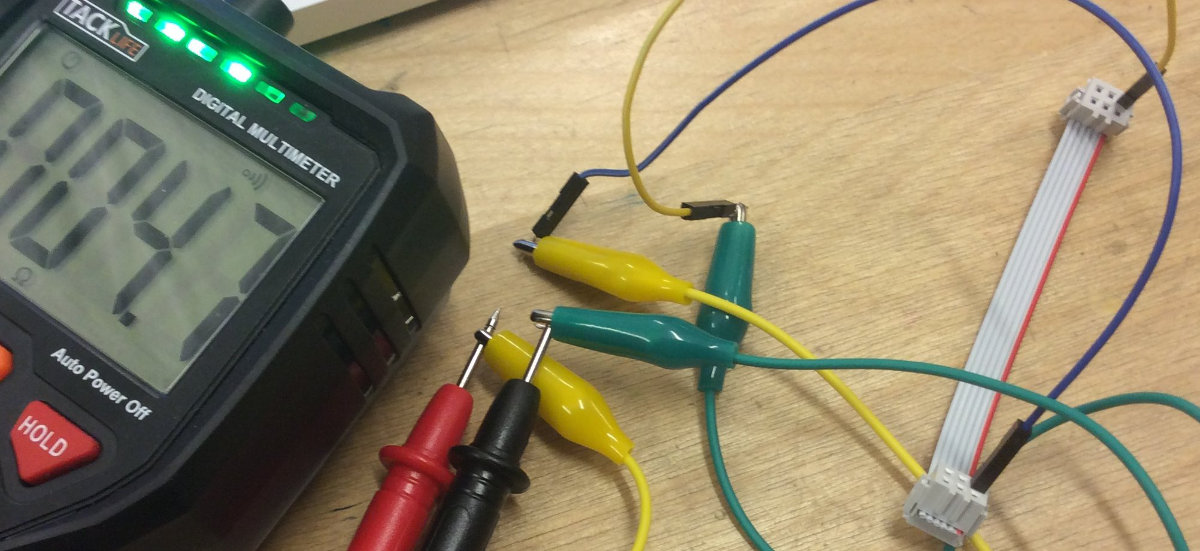
I then checked to see if everything was ok.
Testing
Whith everything done so carefully, I was ready to connect the board to a computer and see if everything was ok. So I connected and... the usb drive was disconnected, indicating a short somewhere. After an inspection, this time by Mathieu, it was discovered that the jumper cable, the one that I didn't like in the first place, was the guilty party. I simply dissoldered it and replaced it with a 0 ohms resistance to act as a temporary bridge.
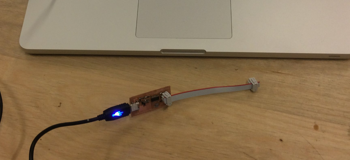
This tiny board will do great things.
Lessons learned on soldering
Soldering is really difficult when you do not have the proper tools. In the lab, there is a big heavy duty magnifier lamp with a fluorescent tube. I though that this would be a big help but I rapidly changed my mind. Once adjusted to your setup, I had to be careful and not touch the lamp otherwise it starts wobbling and with the magnifying effect, I get dizzy.
I was thinking for the next soldering session and in no way I wanted to repeat this experience. I searched the Internet for a solution and found a tool that seems promissing: a headband magnifier with led. This tool will greatly improve the quality of my soldering.
The FabISP, finally done
I was never able to connect the previous board. Neither my teamates. So we changed the board model and made this one instead.
Just in case, because we had lost so much time trying to make a functionnal board, I made many boards for me and George. I soldered the parts and it went straightforward. Note: follow carefully the instructions here!. I considered the board done after a visual inspection and checking all the connections with a meter.
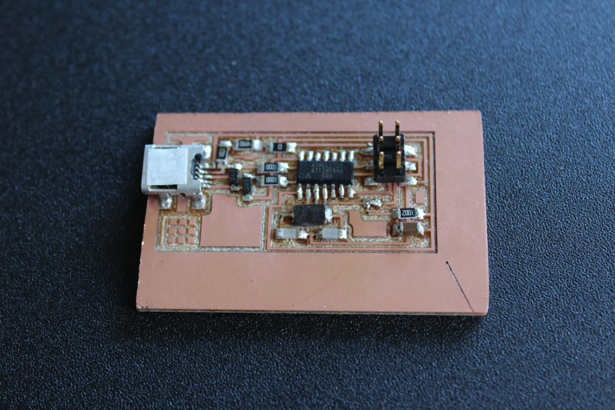
I was really nervous when I first connected my board, as I was afraid of another failure. But I made the necessary connections by hand, doubled tripled checked every connections that I made before finally powering the board.
I passed the smoke test!
Arduino as ISP
I used Alec Matthewson's work on the FabISP as a guide, carefully connecting RST, MOSI, MISO, SCK and the VCC and GND.
I uploaded the ARDUINO ISP sketch, included in the Arduino software. Then it was time to modify the makefile. As per Alec's recommendation, I modified the appropriate line for my setup and hashed the previous two lines.
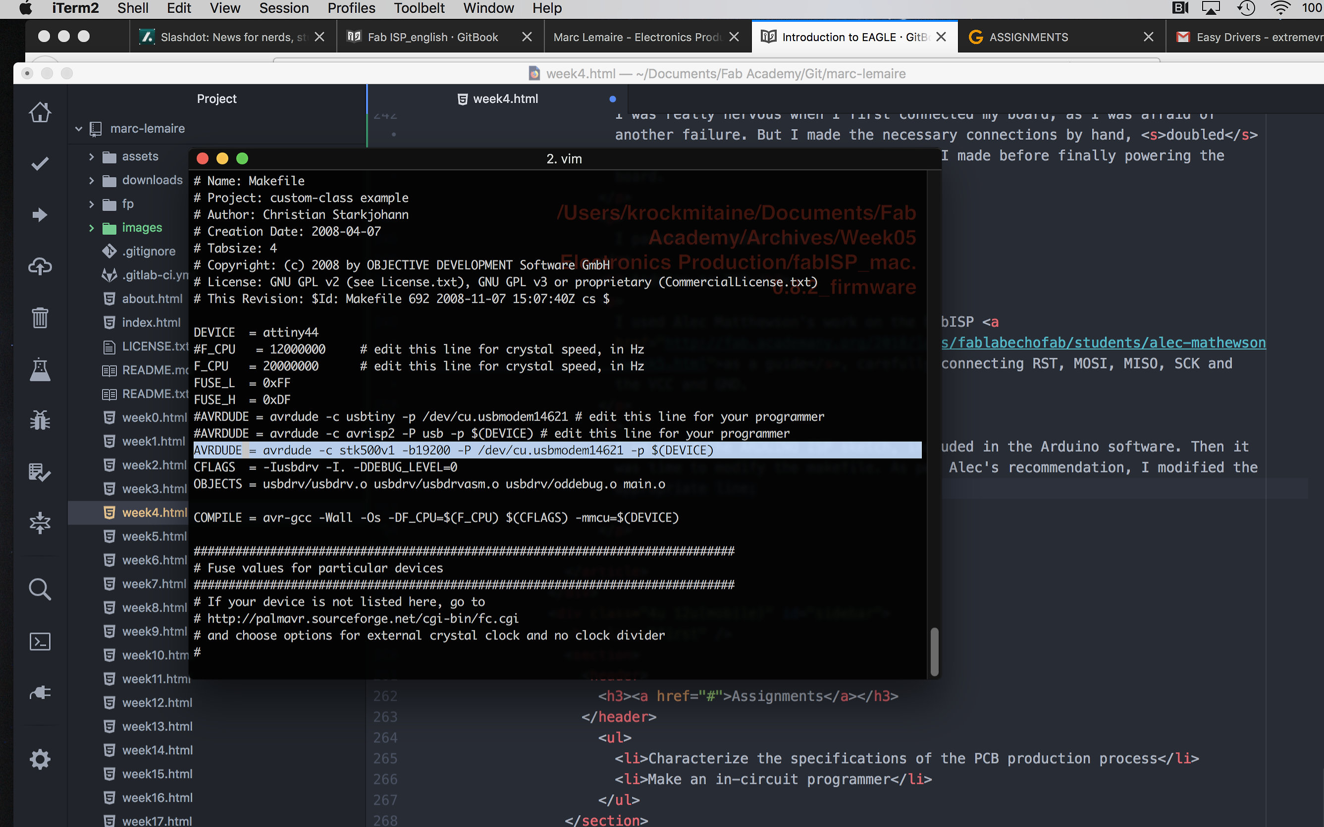
Make clean
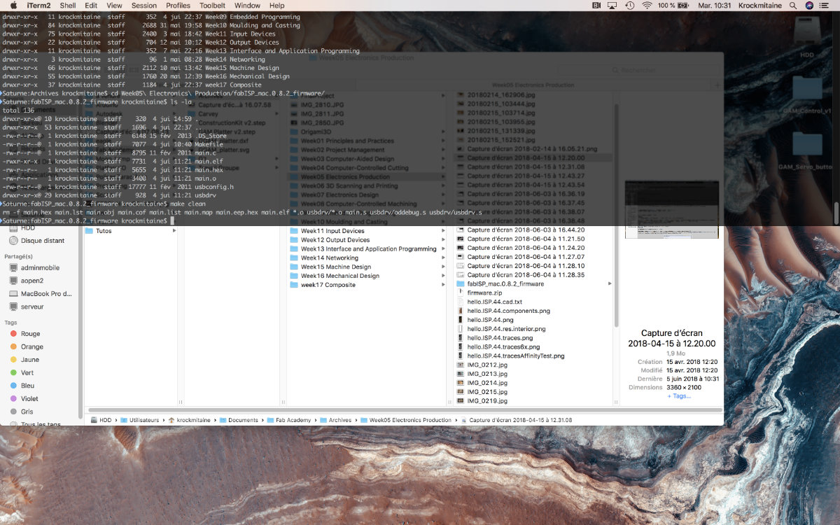
Make clean went without any problem
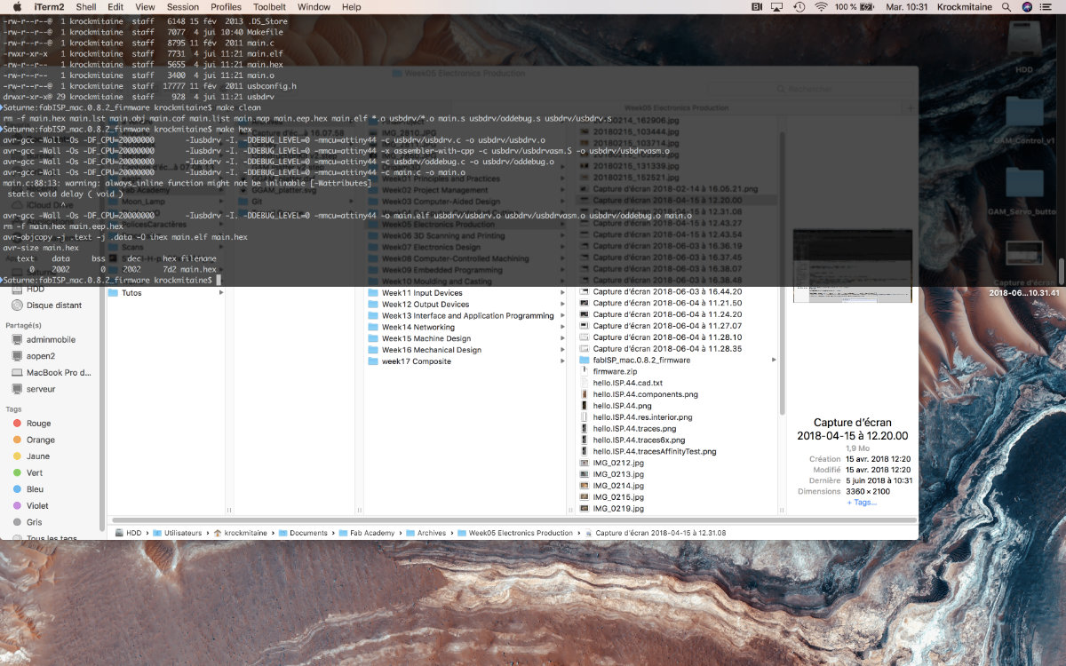
Make Hex
A second success
Make fuse
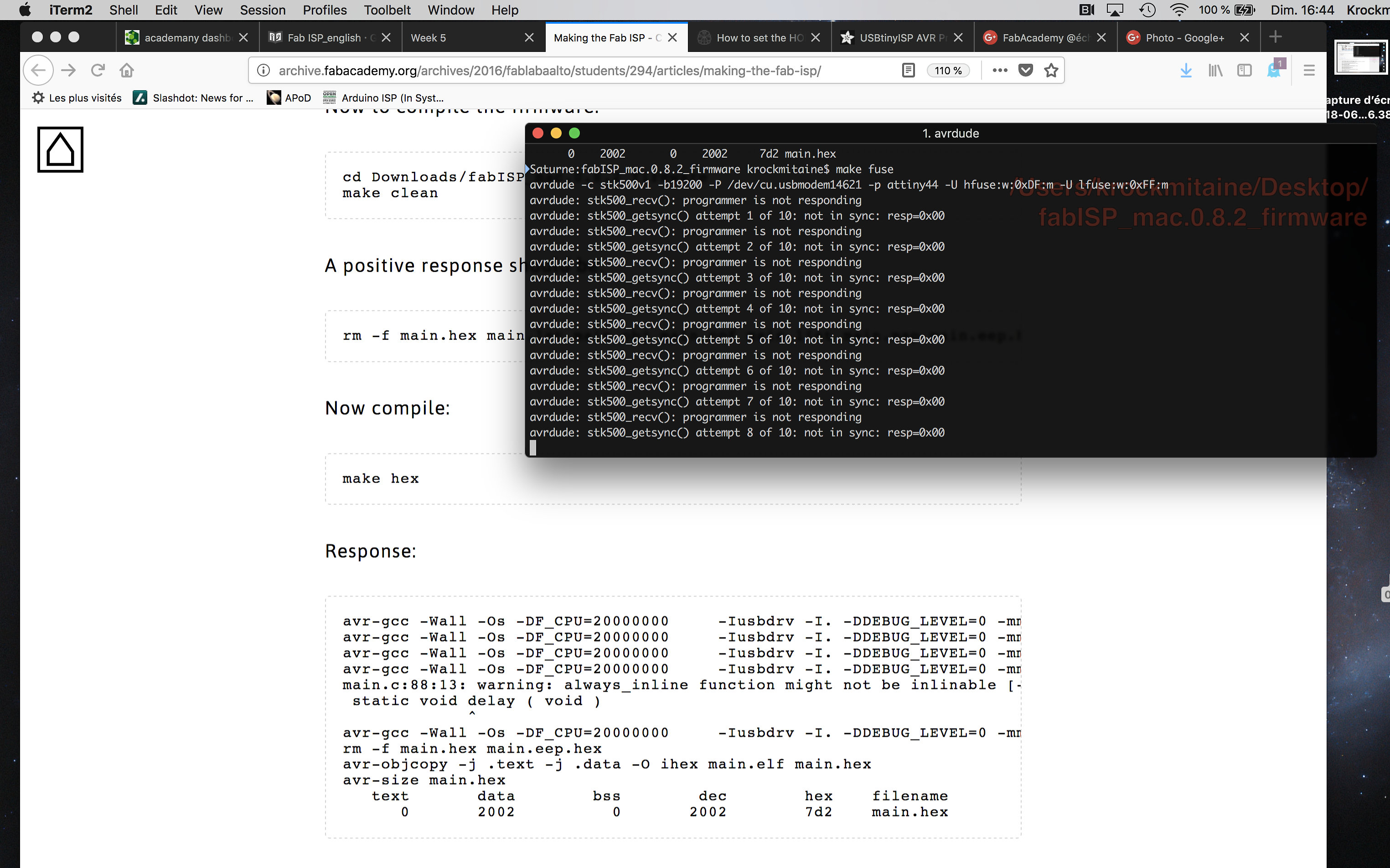
Oh Oh!
This one step didn't go according to plan. I received a "not in sync" error. I verified everything, tried again but always came up with the same message. For once, I put everything on hold and waited for the next day for help at the lab.
The following day at the lab, I repeated my process, again with the same error. As my instructor suggested, I changed the Arduino board. Then I was really puzzled as I started to get error messages on the provided ArduinoISP skecth provided! Trying to isolate the problem, I uploaded the Blink sketch to see what's going on. The sketch uploaded but there was no blinking led!
I then changed tactic, switching my Mac to a Windows machine at the lab. I then uploaded a blink sketch and the board responded with a blinking led. So, back to square one and try find what's going on.
Serendipity
While browsing the Week 4: Electronics Production tutorials here, I stumble upon this Note: This step needs to be done while the Arduino is still not connected to the board you need to program, or you will get an error. ...and I've been doing all this while my board was connected! So, I disconnected all the wires and uploaded the Arduino ISP sketch to the board. I then switched back to my computer.
When all goes according to plan
I then went back to Make clean, Make hex. I then hold my breath and typed Make fuse
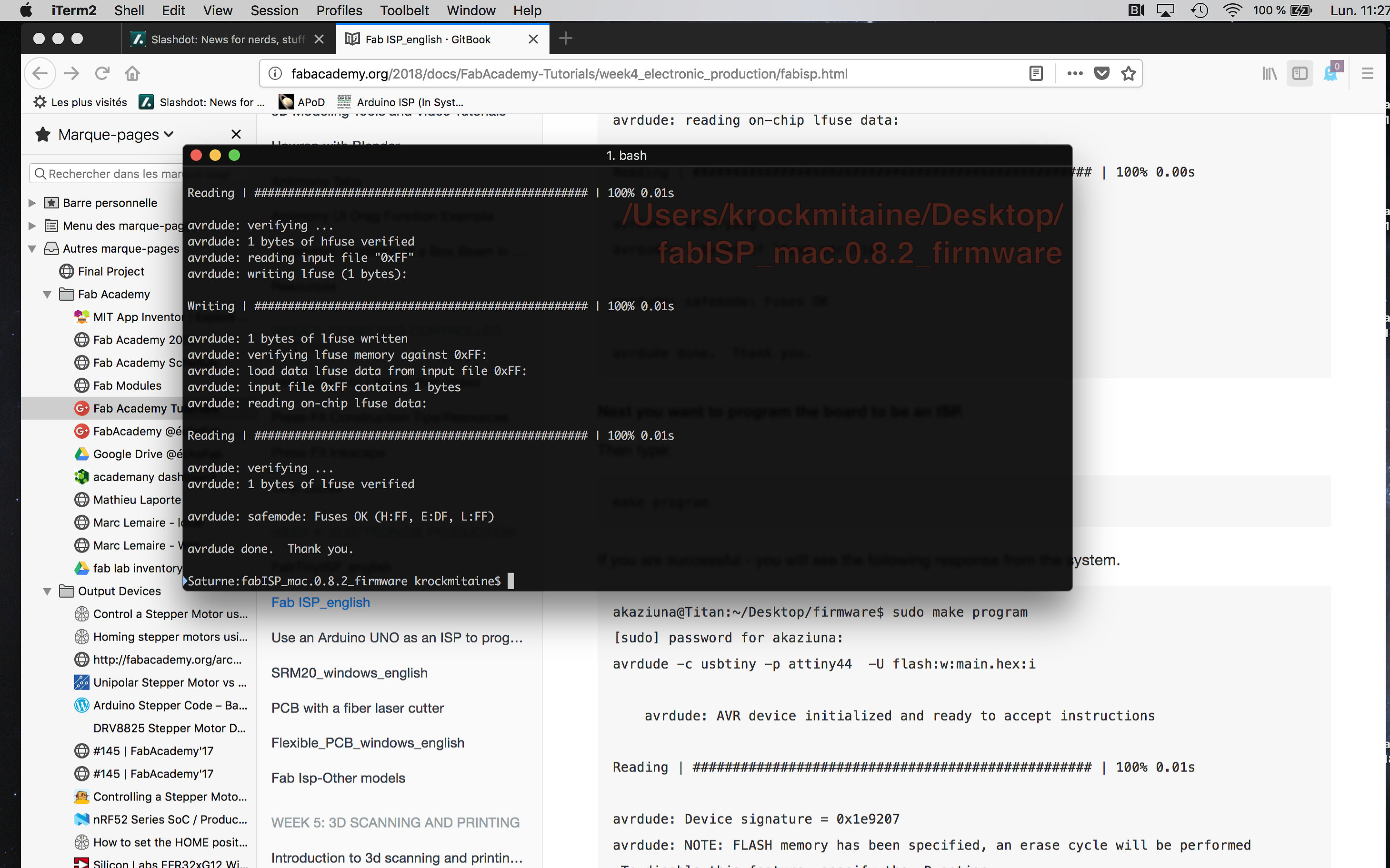
I went up in joy! Was so happy that at last, all that work paid off. So happy that I almost forgot to type the last and most important step:
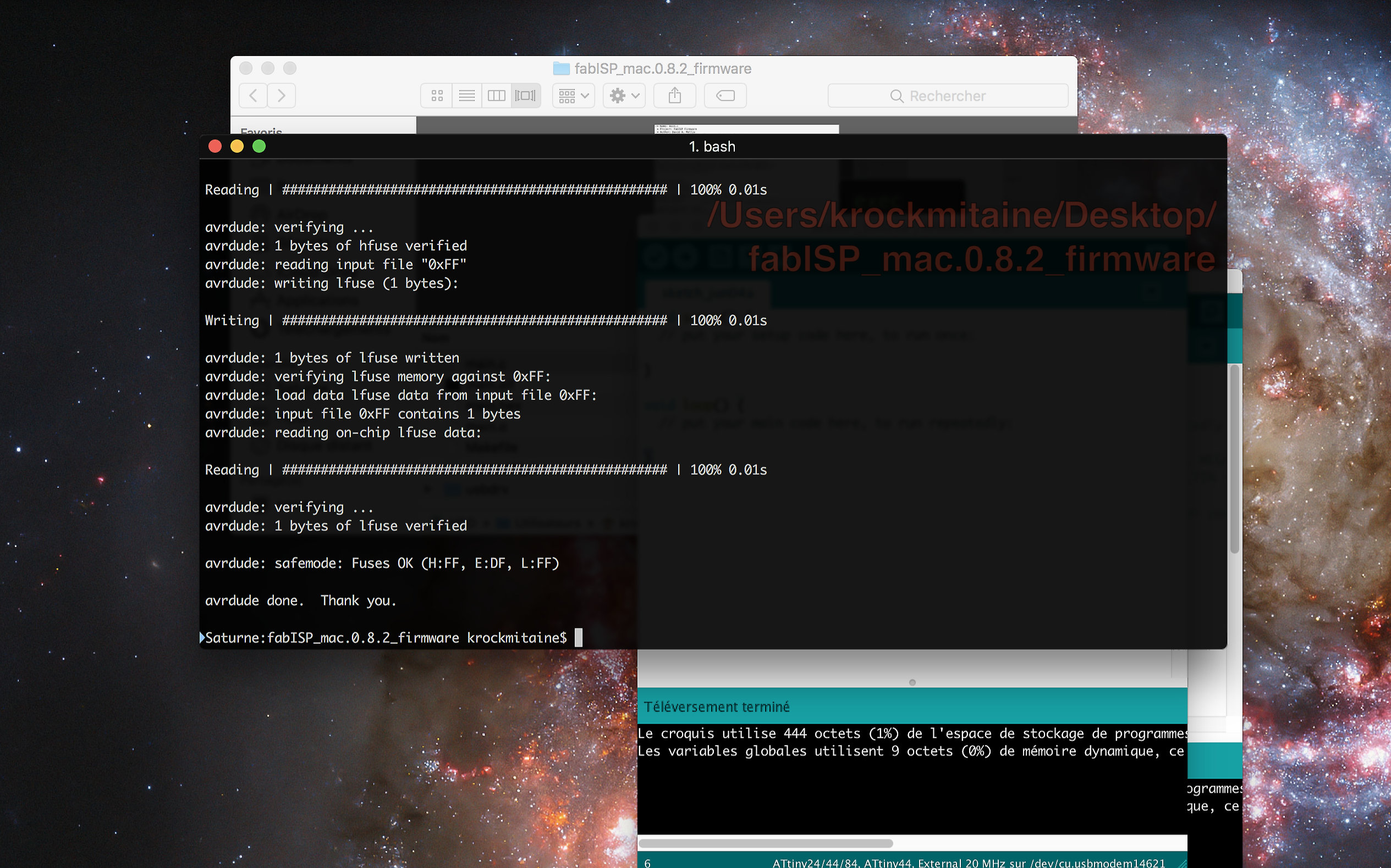
Make program wrote with no trouble at all! Yippeee!
Then for the first time I saw the FabISP in my usb ports.
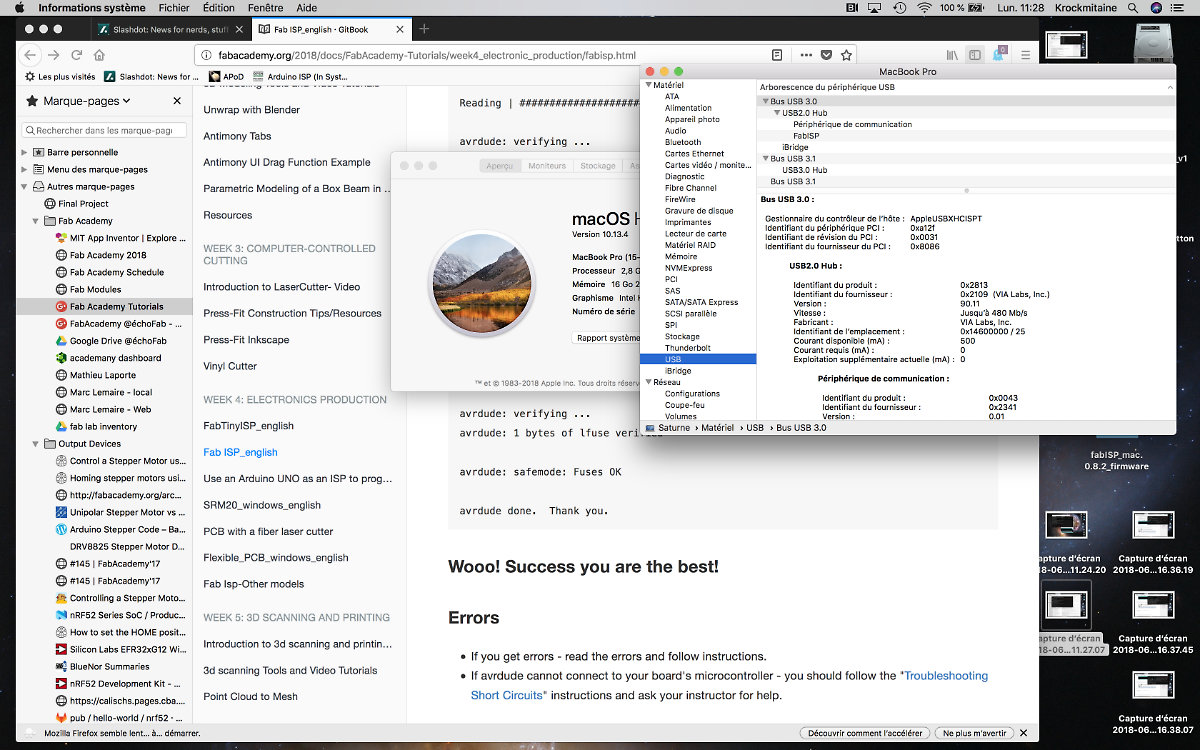
One last task remained before finishing the FabISP: remove the bridge so that I don't reprogram the FabISP by accident.
DONE!
Last comments
At last, FabISP is working and I can go on other assignments. After so many frustration I was elated. I hope that success will be followed by many others as there is still many other tasks to do and soooo little time.
