Attending the Fab Academy in Barcelona, I document each week of intense learning as I come across new digital fabrication techniques.
This documentation is as much a report of what I do as a reflection on why I do so, and will hopefully guide me back to Oceania to spread and make good use of the knowledge gathered along the path.
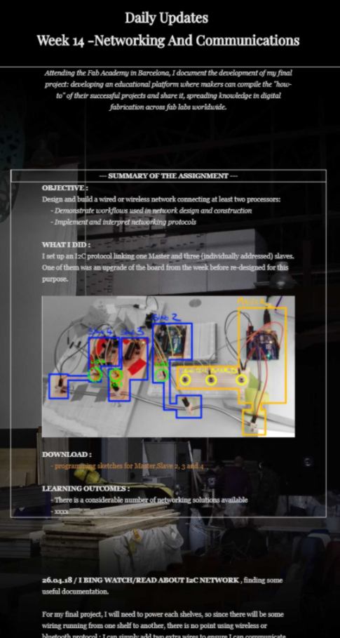
--- summary of the assignment ---
objective :
Design and build a wired or wireless network connecting at least two processors:
what I did :
I set up an I2C protocol linking one Master and three (individually addressed) slaves. One of them was an upgrade of the board from the week before re-designed for this purpose.
I also designed and fabricated a set of two slaves PCBs and one master PCB to set up a similar I2C network.
download :
Learning outcomes :
26.04.18 / I binge watch/read about I2C network , finding some useful documentation.
For my final project, I will need to power each shelves, so since there will be some wiring running from one shelf to another, there is no point using wireless or bluetooth protocol : I can simply add two extra wires to ensure I can communicate with all my microcontrollers.
An issue I might have to overcome is related to the distance between microcontrollers : the I2C protocol was intended to be used within a small range : for laptops, mobile phones... and it might not work at long distance. Looking into it, I found some readings where this protocol has been used for microcontrollers located a couple of hundred meters apart. There is a trick to it. I simply keep it in mind for now.
There is a plethora of information about the topic : Sparkfun has a good tutorial and covers it in depth, comparing other protocols. The wire library is available online. There is also this very well made tutorial that sheds even more light on the topic.
What I intend to do is duplicate my board, and have 4 wires (GND,VCC,SDA and SCL) going from one board to another, all connected to a master board. How the master board will receive and push its data to the slaves is still unplanned - for the purpose of this exercise, I will use an arduino.
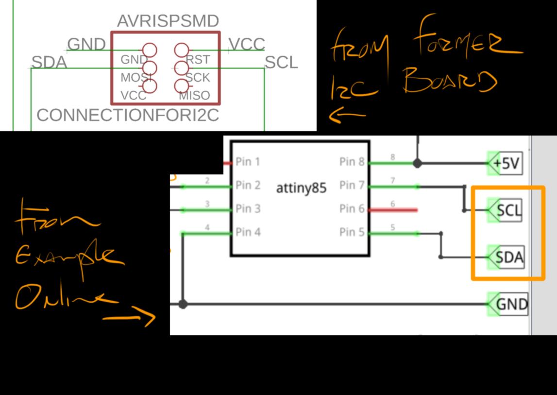
I noticed that during the class yesterday, this network was set up using the ISP headers of the board. I know that it is possible to do so with ATtinies due to their pin configurations. But what about ATMEGA328P? Unfortunately I cannot find anything that points in this direction online. What I can do, however, is to setup a 3x2 header that will be connected to the 4 connections I require.
I open Eagle and modify my board accordinly. I also correct the pins for my servo and buttons, and give myself a little more room to solder the oscillator and its couple of capacitors :
With an instructor we have a quick catch up and demo about I2C, reinforcing the basics :
27.04.18 / I mill, solder and stuff my new board, then set it up with the old one and an Arduino for I2C network protocol. On the way, I got some new microcontrollers and extra toys :
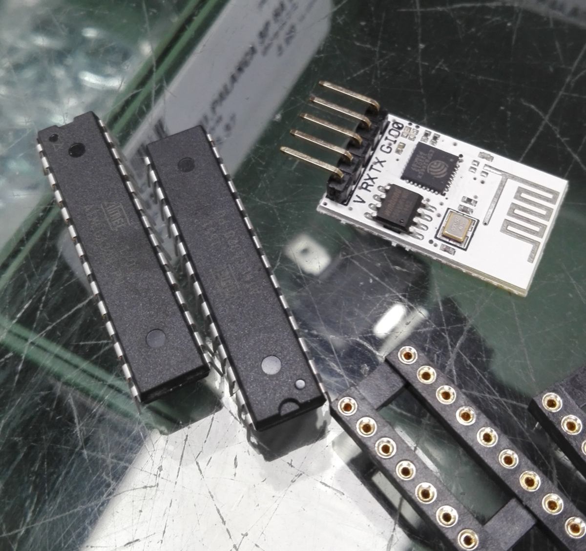
This time I bought some sockets so I can re-use my microcontrollers for other boards and projects in the future.
To bootload these ATMEGA328 (which differs from the ATMEGA328P), I follow this workaround. I then set things up according to this tutorial.
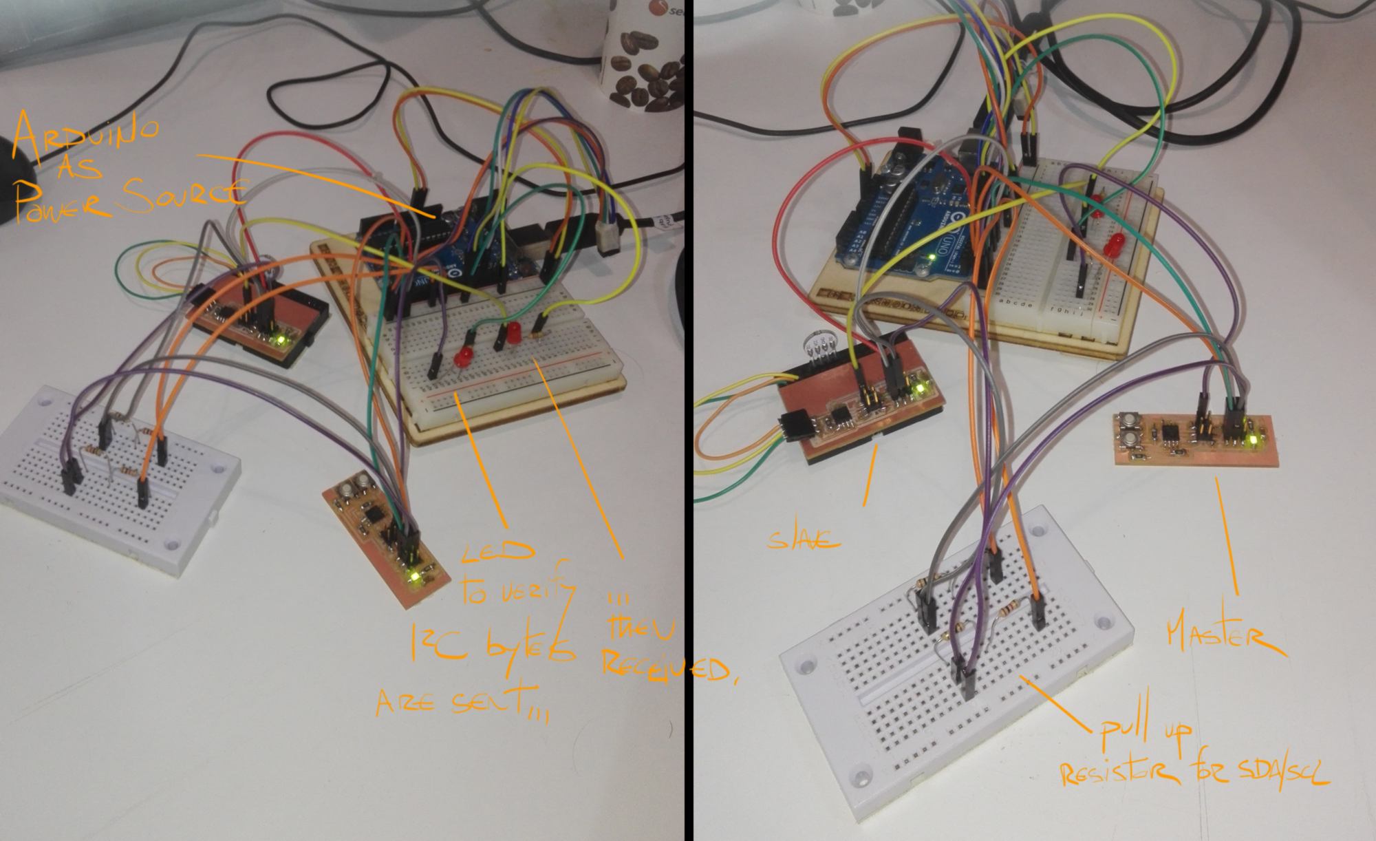
I set up all my boards ready for I2C network :
I plan on finishing this project over the weekend. However while discussing my setup with Guillem, and bringing forward the potential issues related to distances, he comes up with another - actually many others - option :
The conversation goes this way :
And this is how I end up with a couple if ESPs in my pocket to play with during the weekend. What I get is a whole module with everything on it. If it is a successful test, I will have to replicate this board and modify it (getting rid of components such as usb connections) that are not required.
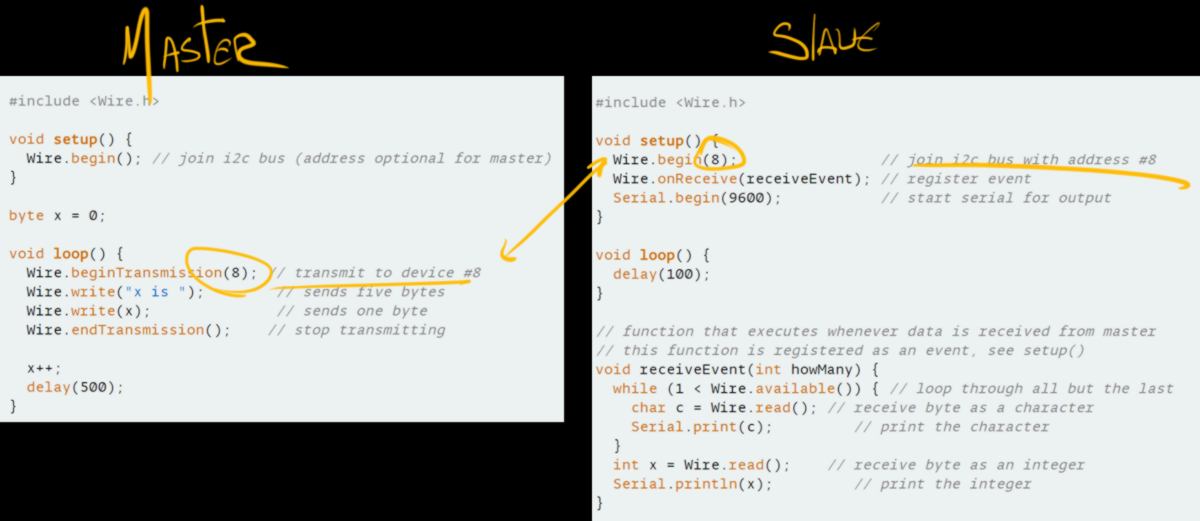
28.04.18 / I2C day today, I attempt to load some code on both chip from this tutorial, one as a master, the other as a slave. Since I do not have a dedicated programer with me I will use an Arduino to bootload and program my boards. I receive an error message while bootloading:
avrdude: Device signature = 0x1e9514 (probably m328) avrdude: Expected signature for ATmega328P is 1E 95 0F Double check chip, or use -F to override this check.
I read in this forum that you can happily lie to the ARDUINO IDE to bootload an ATmega328 :
"If this is your problem, you can probably temporarily change the "uno.build.mcu" in boards.txt from "atmega328p" to just "atmega328" and burn the bootloader. Then change it back, because the bootloader will happily lie to the Arduino IDE and claim to be a 328p."
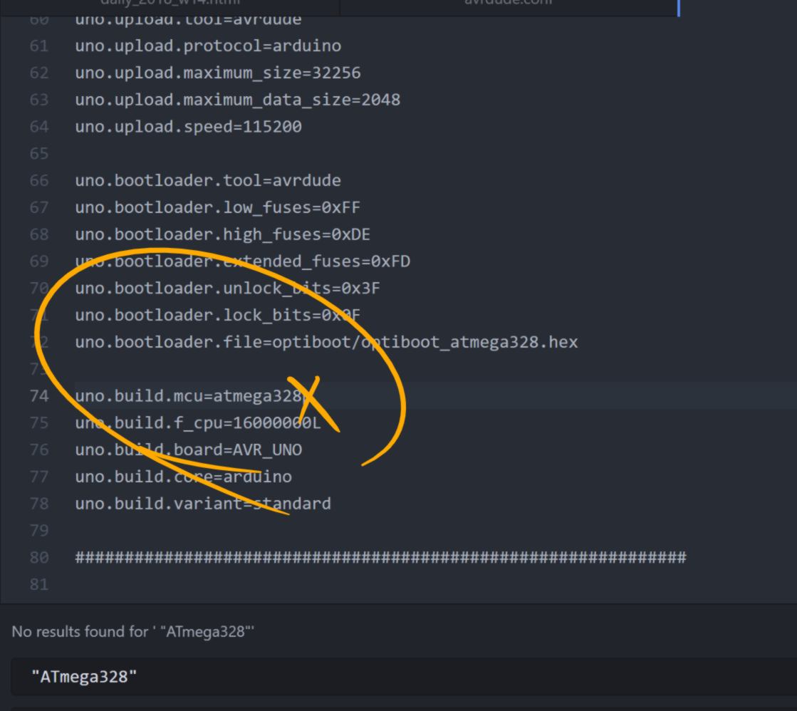
Let's try it. The chip gets bootloaded. I load the slave program while I am at it, then revert the boards.txt back to its former version and upload the master program.
I then have a look at the serial monitor of the slave microcontroller. In this code, the Master is programmed to send 6 bytes of data every half second. Once that message is received, it can then be viewed in the Slave board's serial monitor window :
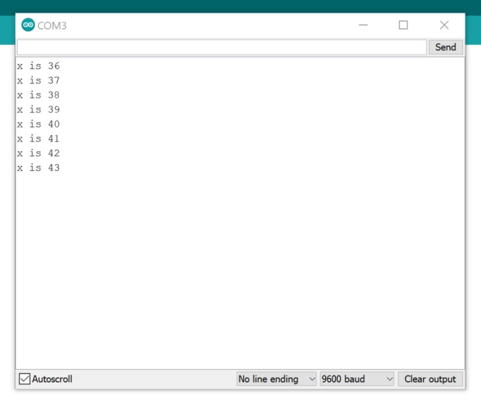
This is working well. The data sent are also uniquely addressed, meaning the Master microcontroller is sending data to this particular microcontroller (called "8") :
This is important since I am going to add an extra slave shortly. First though, I will change the behavior of the slave. I wish to get a NeoPixel to light up as a result of a command sent from the master. I am goin to modifiy both codes.
Firstly I write a code where a button changes switches a Neo Pixel on and off. I merge the button tutorial with the simple neopixel tutorial.
Then I modify both master and slave code to integrate this update, and upload them (switching the boards.txt file everytime I upload the ATmega328). No NeoPixels turns on. I check the serial of the slave, which returns some random numbers :
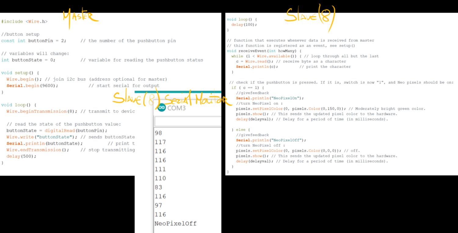
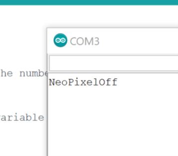
Well I realise I am actually sending the word "buttonState" through I2C. Not quite the objective here. I get gid of the double apostrophe and load the code again. The result in the slave console is minimalist :
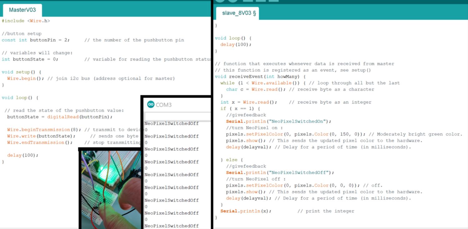
To test my code, I need at least one side (either Master or Slave) that is functional. I revert back to the original I2C tutorial. I can easily verify what my Master sends through the slave serial, so I add the part of my code related to the button and use the variable generated as data sent through the I2C. I works. I then add my if statement to the slave code, triggering the NeoPixel to be switched on if the slave "reads" a specific value (here"1). It works:
The next step is to add an extra microcontroller to the setup. I first need to modify my master code so it sends input to another microcontroller using another button, and duplicate my slave code :
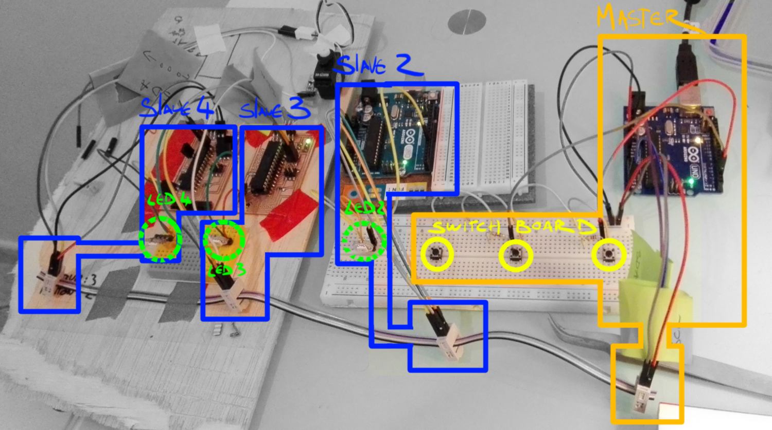
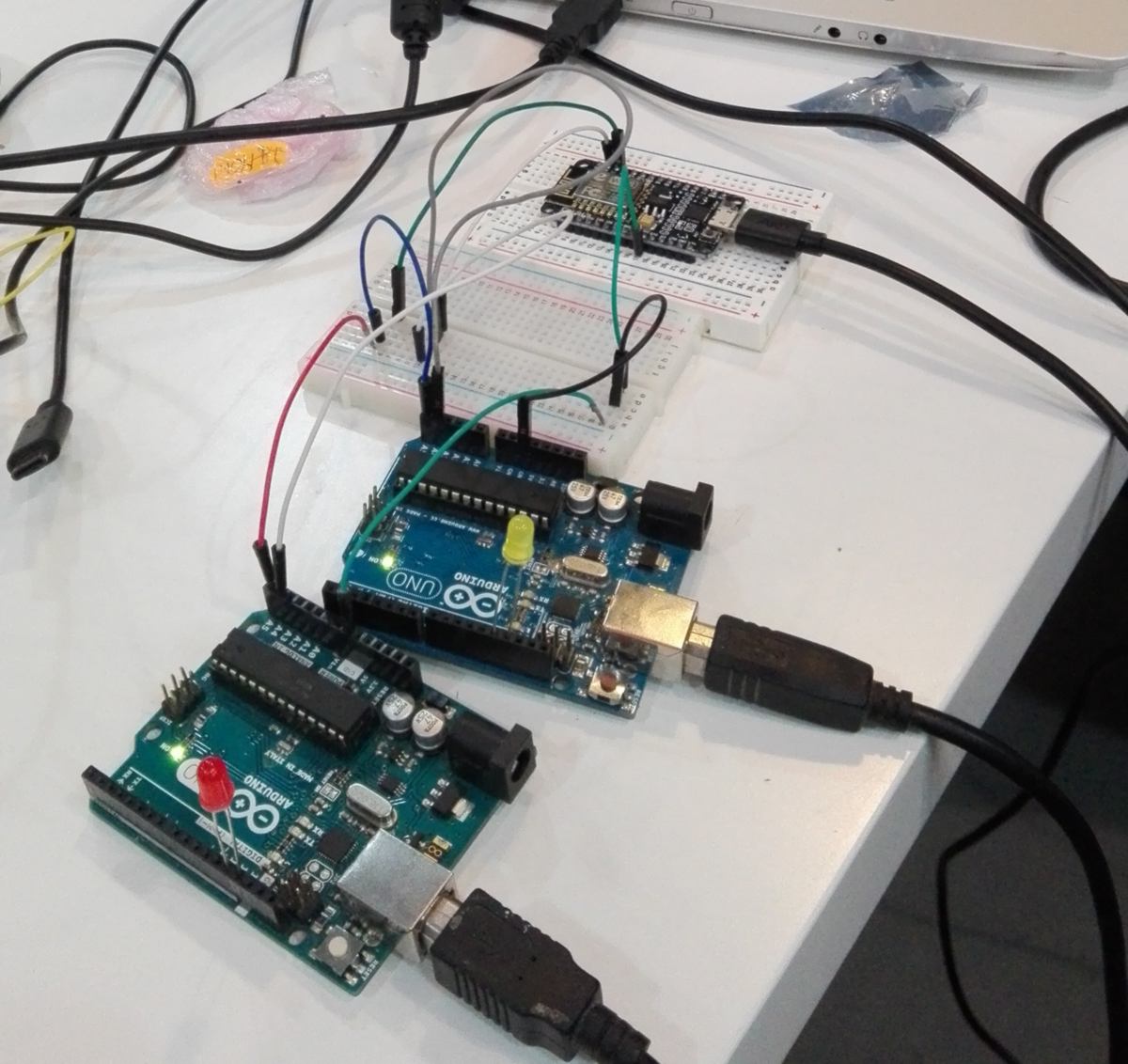
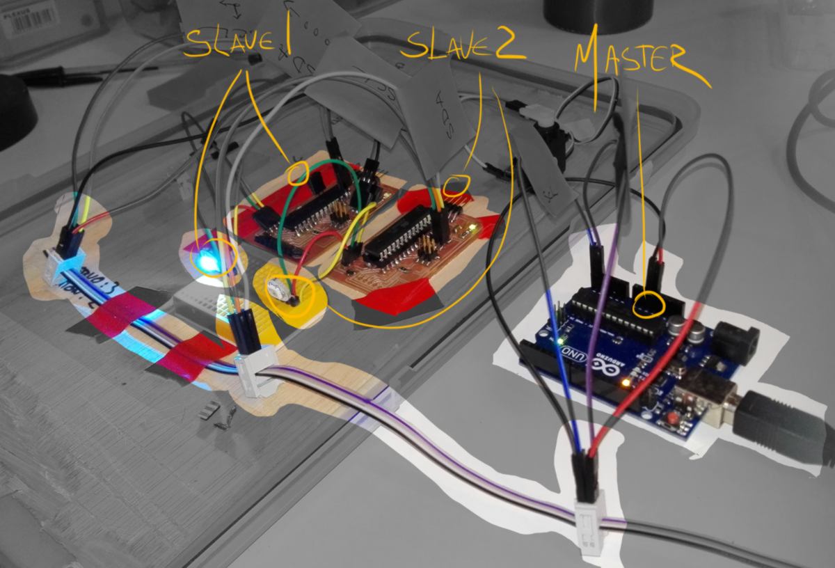
I then attempt to connect all my microcontrollers together, but when switching the USB on on my computer, the lights slowly switches off. Since I also use the arduino as a programer, there is a fair amount of wiring on the table, and I might have made a confusing mess somewhere. I do a bit of clean up, and here is our first network using I2C protocol :
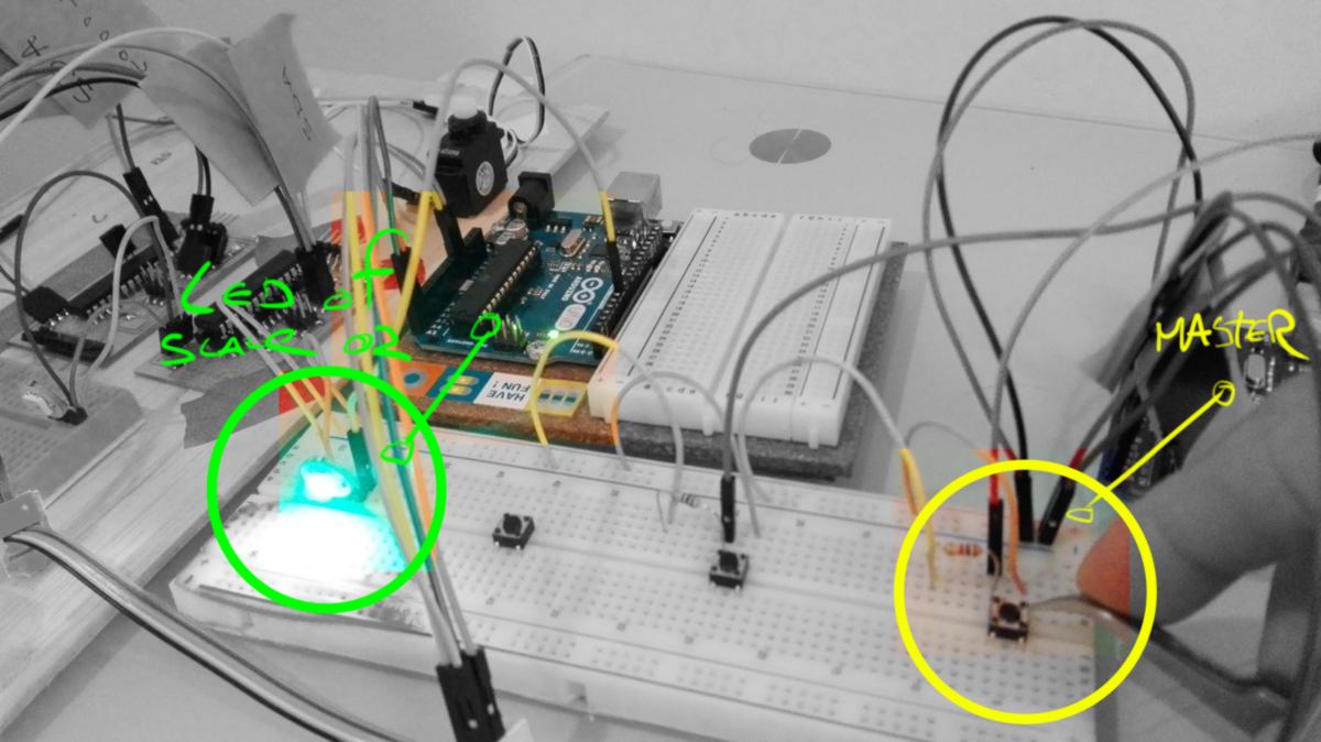
I have yet to upload the sketch for slave #4 (microcontroller on the left-hand side). However the setup works, I added an extra arduino as a slave to prove the point that I2C allows connexion between many devices at once.
On Monday, I will test how far away can these devices be located.
Until then, I add an extra "summary" section to each of my assignments to make life easier for my tutors :
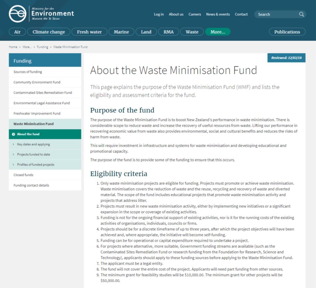
I also look at a Waste minimisation and Innovation fund, closing in 40 hours. I am considering applying for a container to fit the Precious Plastic kit. I will let this one slip away, since I have noticed a larger "waste minimisation fund" opens tomorrow which gives me 14 days to act. It is also a national fund, meaning it might be worth discussing with other labs in New Zealand about this project.
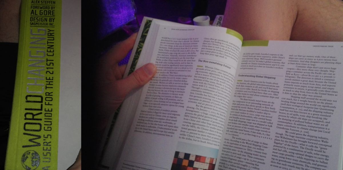
30.04.18 / Over the weekend I go back to an exhibition I went to before, and find an interesting book. This book was located on a shelf in a room that was part of the exhibition. This room was a representation of a kitchen in a post-oil era, sending the audience 30 years in the future. The book itself has already been released though, and was full of very interesting comments and projects that are happening now, also mentioning the Fab Network :
Back at the lab, I attempt to connect all my slaves and my master using a cable reflecting the distances between learning kit of the shelves. Each node will be 60cm apart :
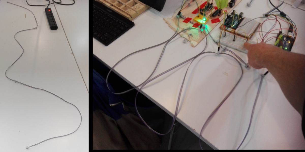
It works just fine.
The suggestion brought upon by Guillem sure sounds appealing, but rather than looking into another protocol, I would rather deepen my understanding of the I2C protocol, and dedicate some extra time to the development of the digital interface. Bye for now, wireless network.
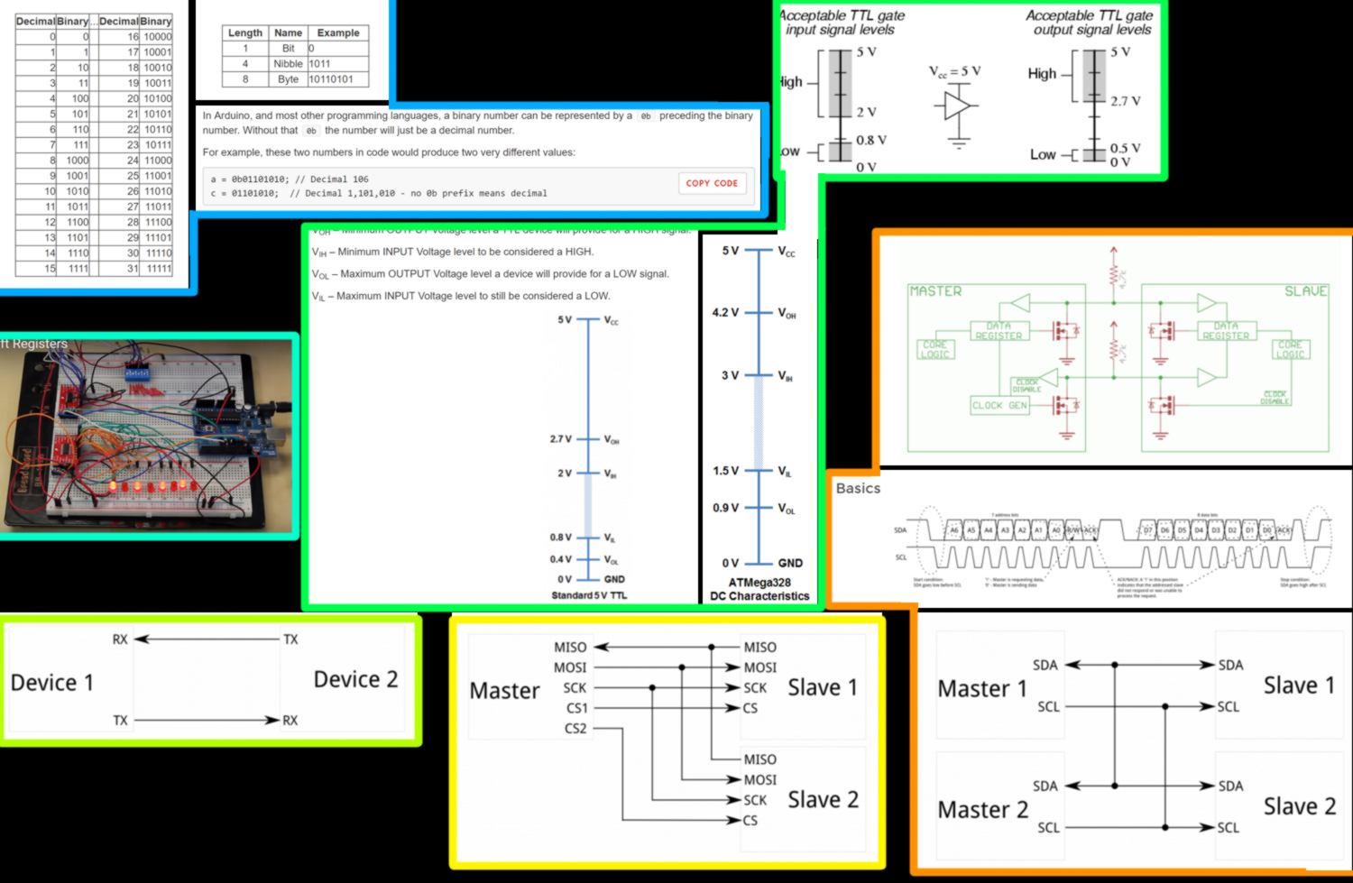
Before moving on I am having a proper read at the Sparkfun webpage about I2C. I learn about binary (which includes a definition of the very quirky word "radix"), shift-registers (very nice video), logic levels, SerialPorts ( inherently suited to communications between two, and only two, devices), SPI (good for high data rate full-duplex, but allows for only one master in the network and requires 4 pins by default plus an additional pin per extra slave), and of course I2C.
I am surprised to hear that resistors are required on both communication lines for communcation to be enabled. One paragraph is particularly relevant to my setup:
"Resistor selection varies with devices on the bus, but a good rule of thumb is to start with 4.7k and adjust down if necessary. I2C is a fairly robust protocol, and can be used with short runs of wire (2-3m). For long runs, or systems with lots of devices, smaller resistors are better."
Perhaps my concern about distances was unfounded.
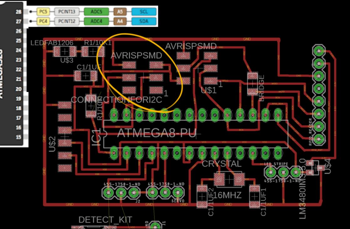
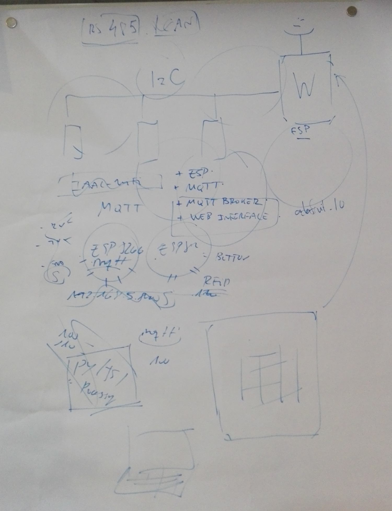
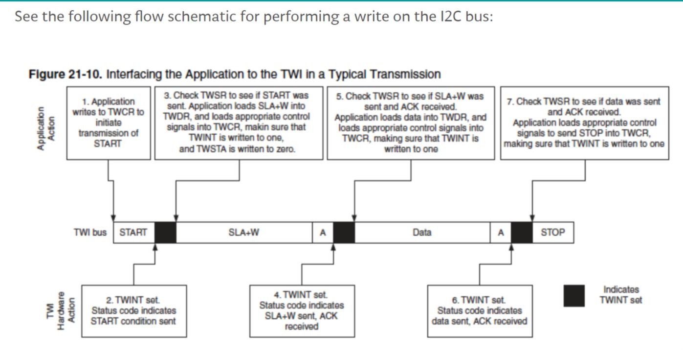
My last read is the Wire library detailed reference, which : " attempts to {...} give the Wire library the documentation it needs and deserves." I learn that on the ATmega, there is a specific piece of hardware, the TWI, that will handle the communication. Some of the documentation is still a bit cryptic but knowing what the general concept is (see diagram below) I get an understanding of how the TWI reacts to the call of different variables.
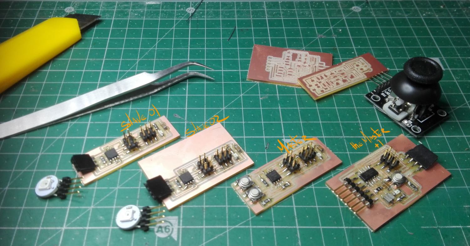
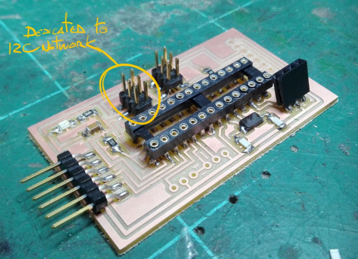
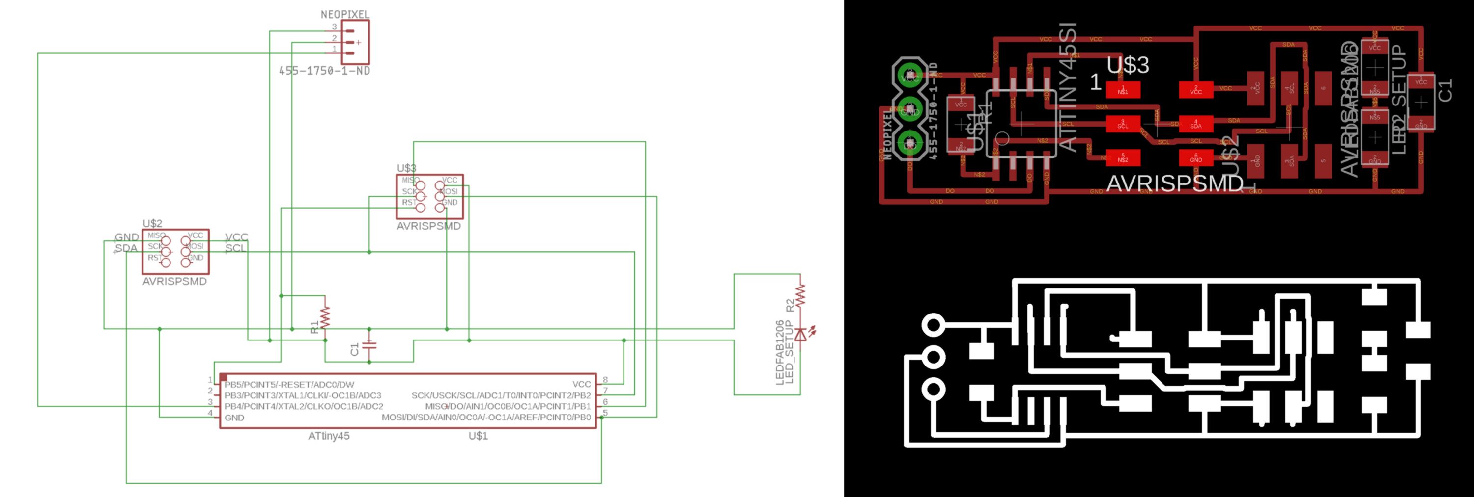
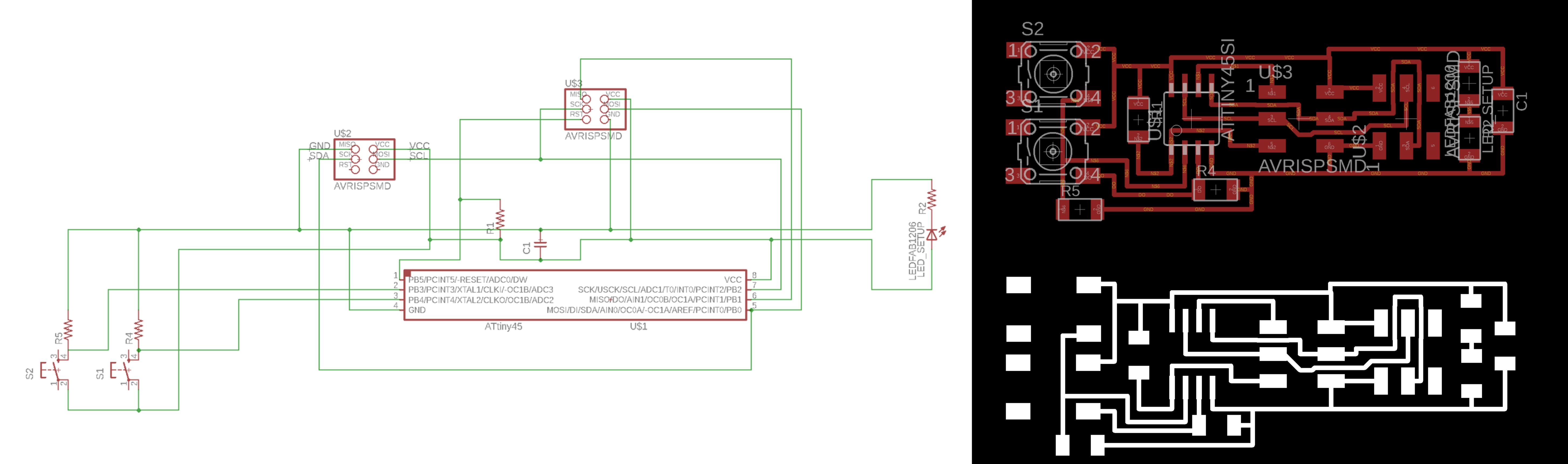
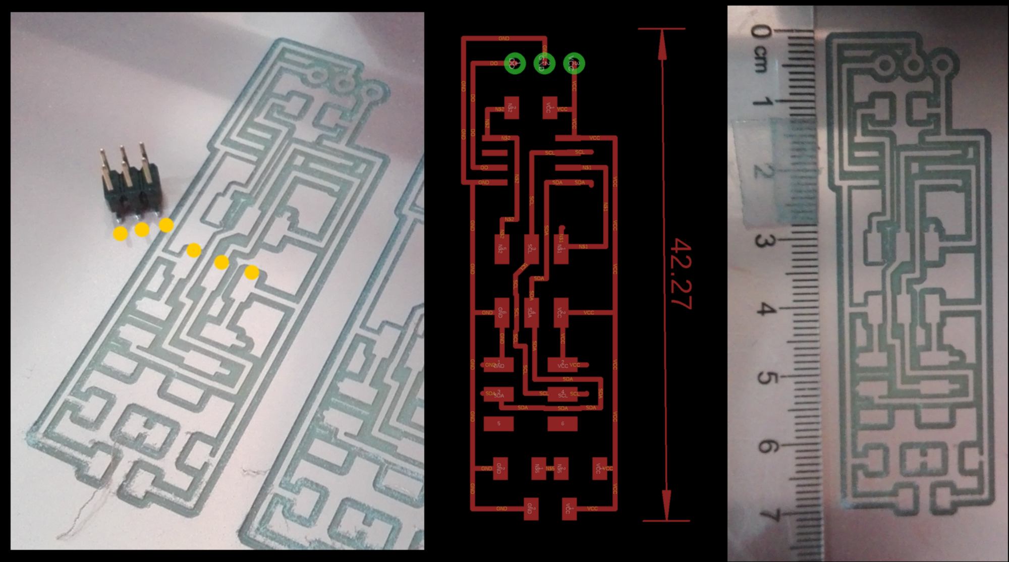
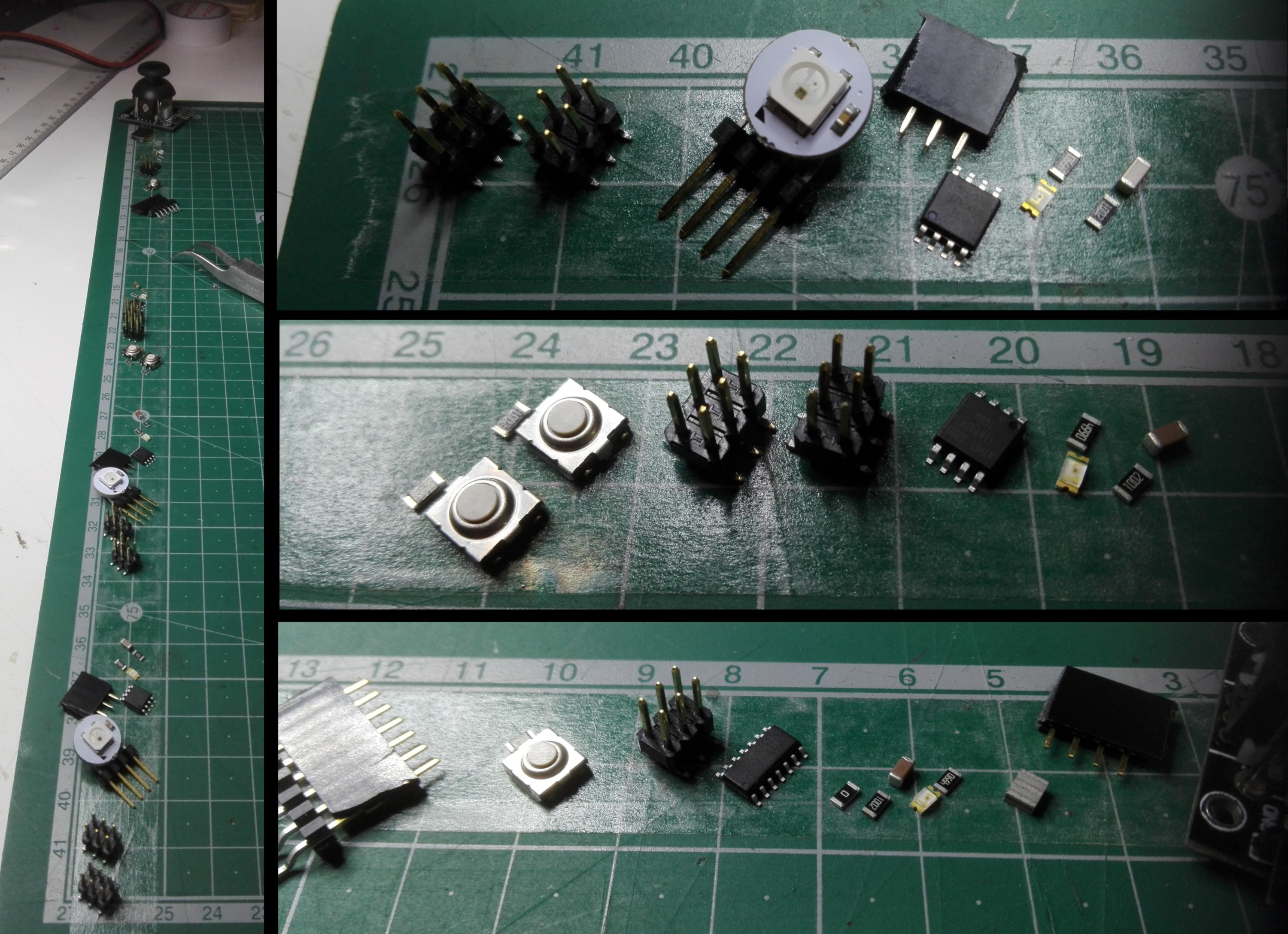
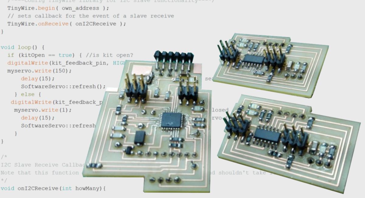
27.05.18 / Last minute addition! I design two PCBs : one master and one slave, to step away from any arduino. I find some documentation and start designing the PCBs :
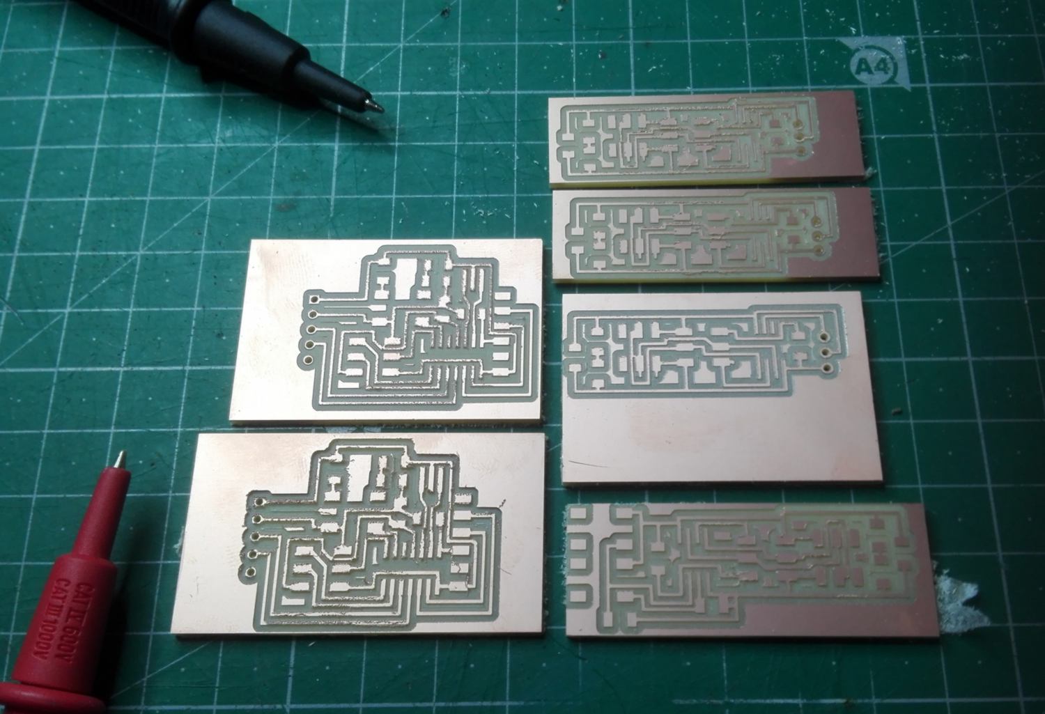
28.05.18 / Last minute addition! I mill a batch of boards :
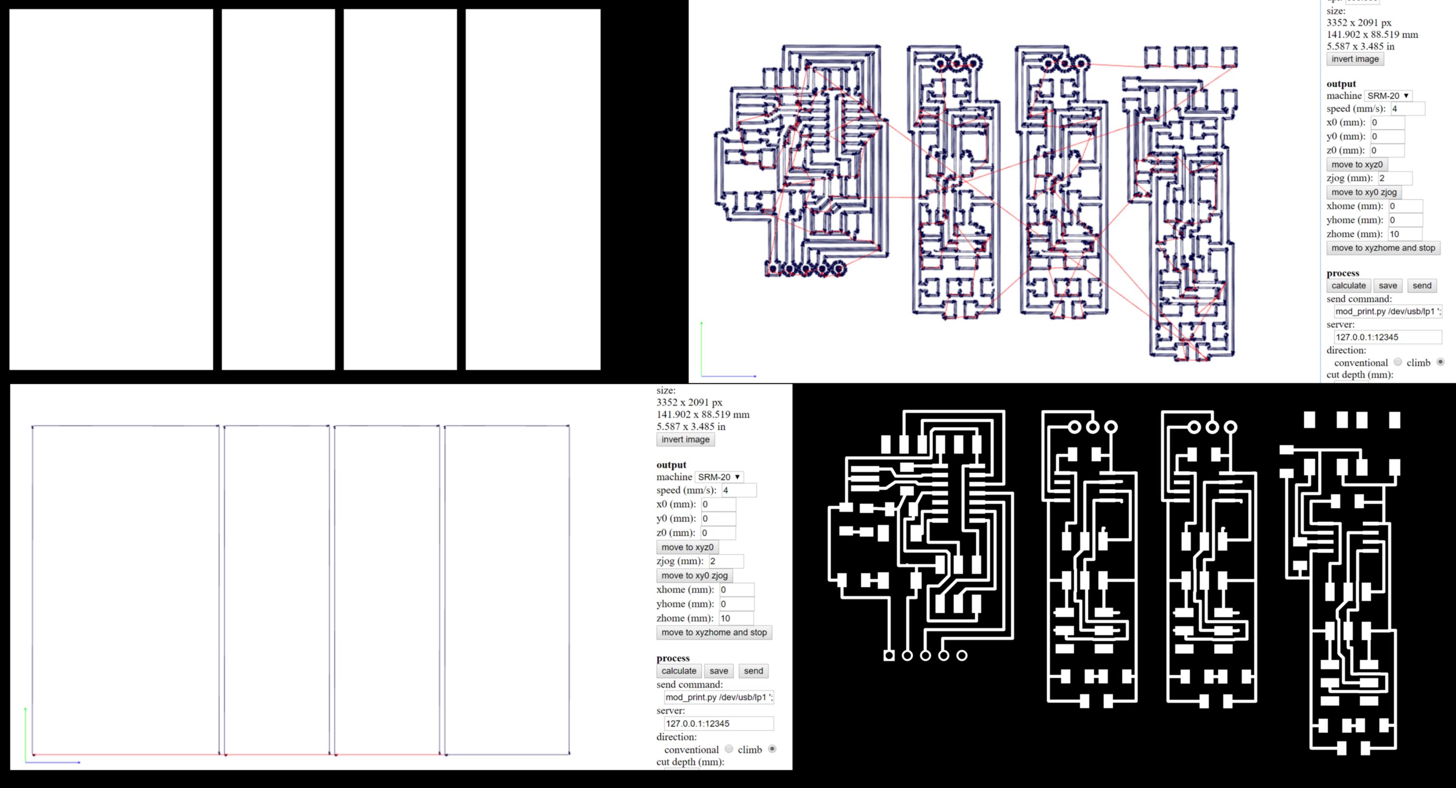
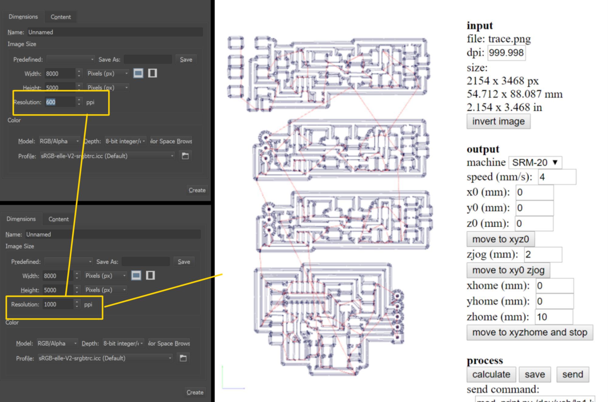
Half way there, I check the dimensions of the board, which look gigantic :
In the process of merging all .png together, I used a blank image with a different definition! I correct it, and start a new batch :
Unfortunately the tracing on two of the boards (at the bottom of the picture below) have been badly traced. Since I have set the origin in Z lower, the end mill has scraped the traces with the toothholder :
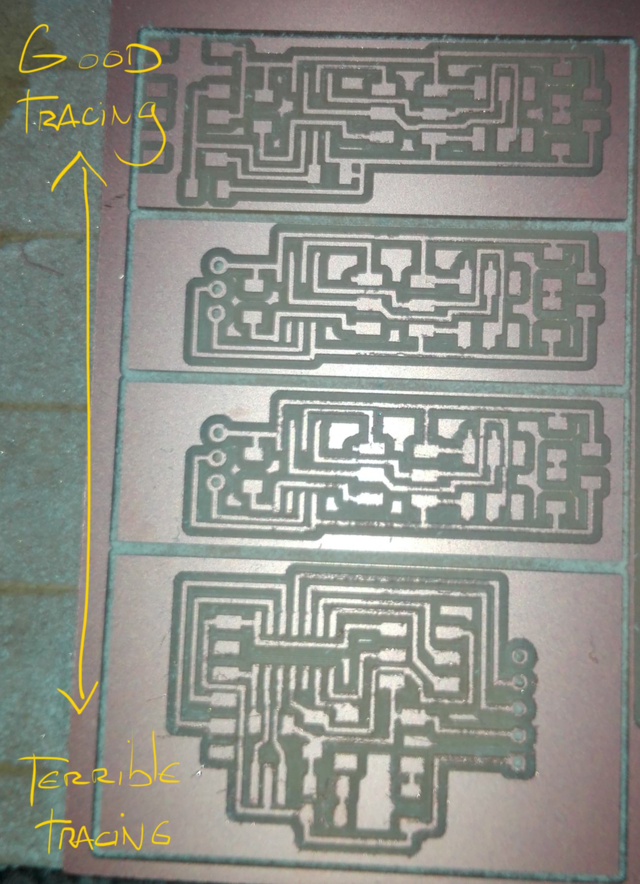
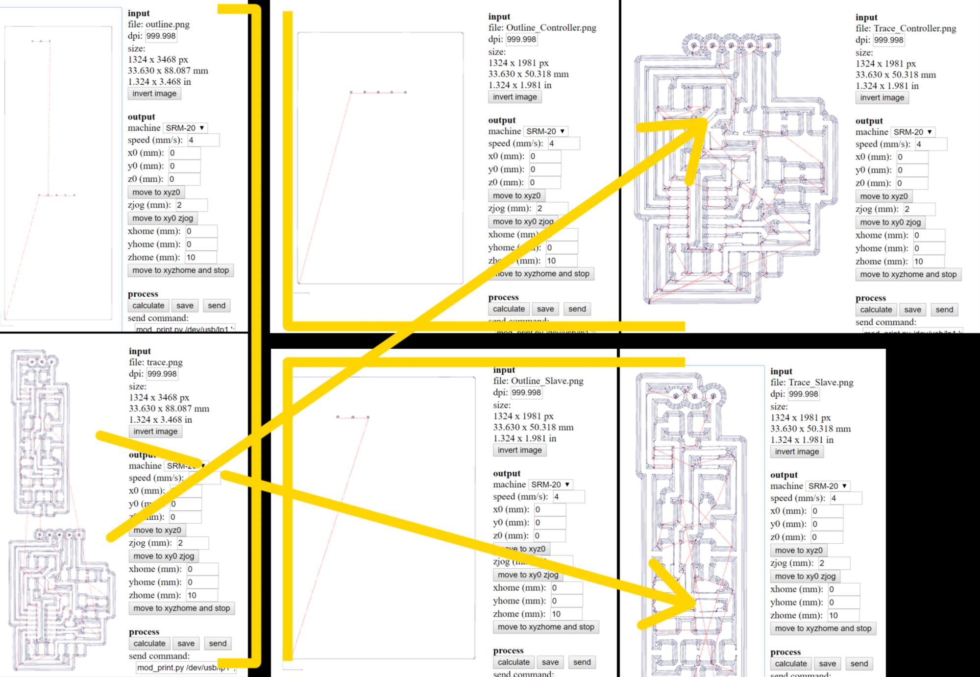
I plan on re-cutting the two boards at the bottom. I prepare the file. However, on the right-hand side of the PCB, the height difference between the front and the back of the bed is even more pronounced. I decide to split the file in two (one per board) and cut them successively, adjusting the z on the lowest point for each of them :
I send the files for milling. In the meantime I have prepared the table for soldering :
29.05.18 / Last minute addition! Today I will document a step forward in the right direction. However I won't fully finish setting up the network today, leaving it for another time.
The cause of the issue I bump across comes down to the following : the library I previously used to set up the I2C network, Wire, is not supported on the ATtiny45. Therefore I have to kiss the easy upload-and-play procedure goodbye. The code previously written for the ATMEGA328 will not be of much use, which is a drawback since I will not know whether issues are code or hardware-related.
Some bullet points of the day :
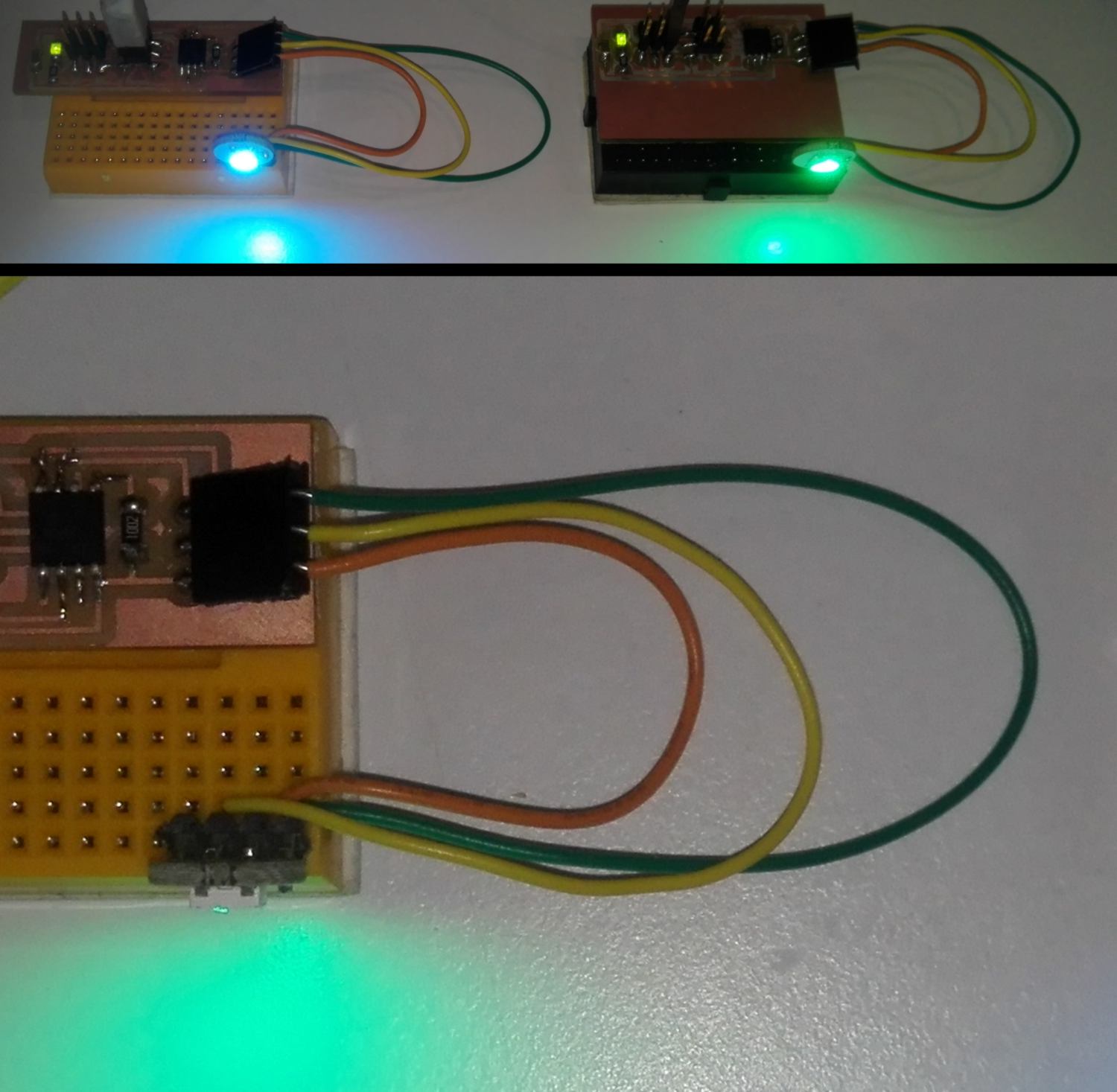
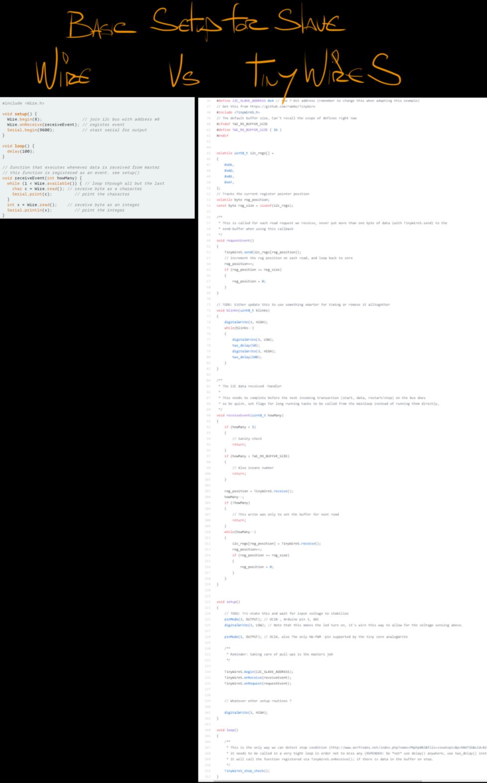
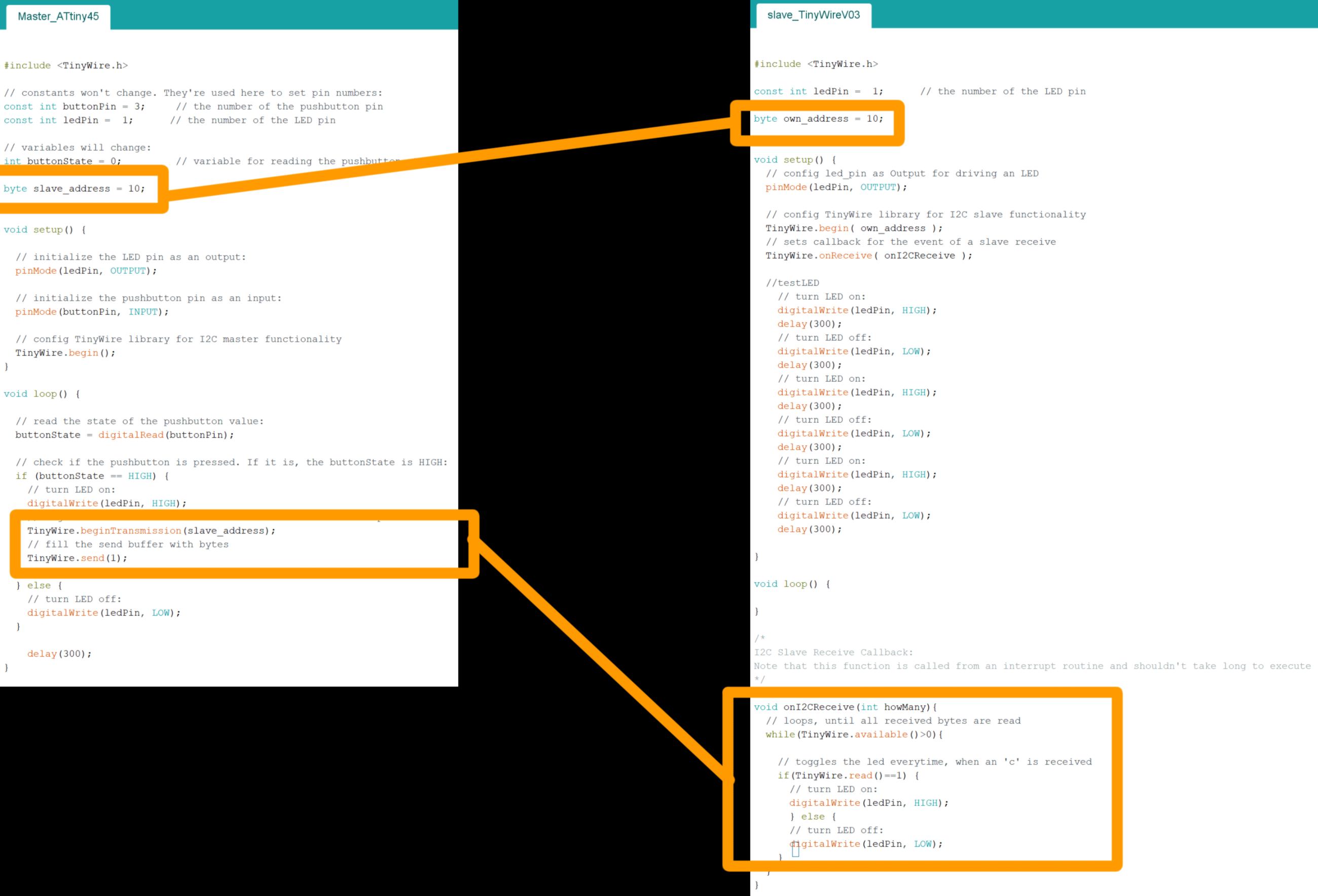
Ideally it would be even better to get a breadboard out, a ATtiny45 fitting on it, and re-design the PCB from there rather than constantly plugging/unplugging wires and programmer. By this time though it is the end of today, and we are left with our setup designed for testing purpose :
I do not think it would take long to do so. However I will leave it aside for now and focus on finishing the other board for the interface programmation as well as my final project. I hope to be able to come back to it later on.
20.06.18 / Last minute addition! My story with I2C network is not over yet. Actually it takes a central place in my final project, and after making specific board for it, based on both ATMEGA328P and ATtiny44, I succeded in creating a network between them :
You can read more about it on the final project webpage .