Attending the Fab Academy in Barcelona, I document each week of intense learning as I come across new digital fabrication techniques.
This documentation is as much a report of what I do as a reflection on why I do so, and will hopefully guide me back to Oceania to spread and make good use of the knowledge gathered along the path.
--- summary of the assignment ---
objective :
Redraw the echo hello-world board, add (at least) a button and LED (with current-limiting resistor), check the design rules, make it (if you have time this week, test it). Optional: simulate its operation. Measure its operation.
what I did :
I designed a board inspired by the hello-world board, adding a switch button and two leds. I programmed and tested it successfully.
download :
Learning outcomes :
01.03.18 /Today, a team of student is presenting researches about adobe printing. This team has developped this technique for architectural purpose, designing a set of bricks with thermoregulating properties :
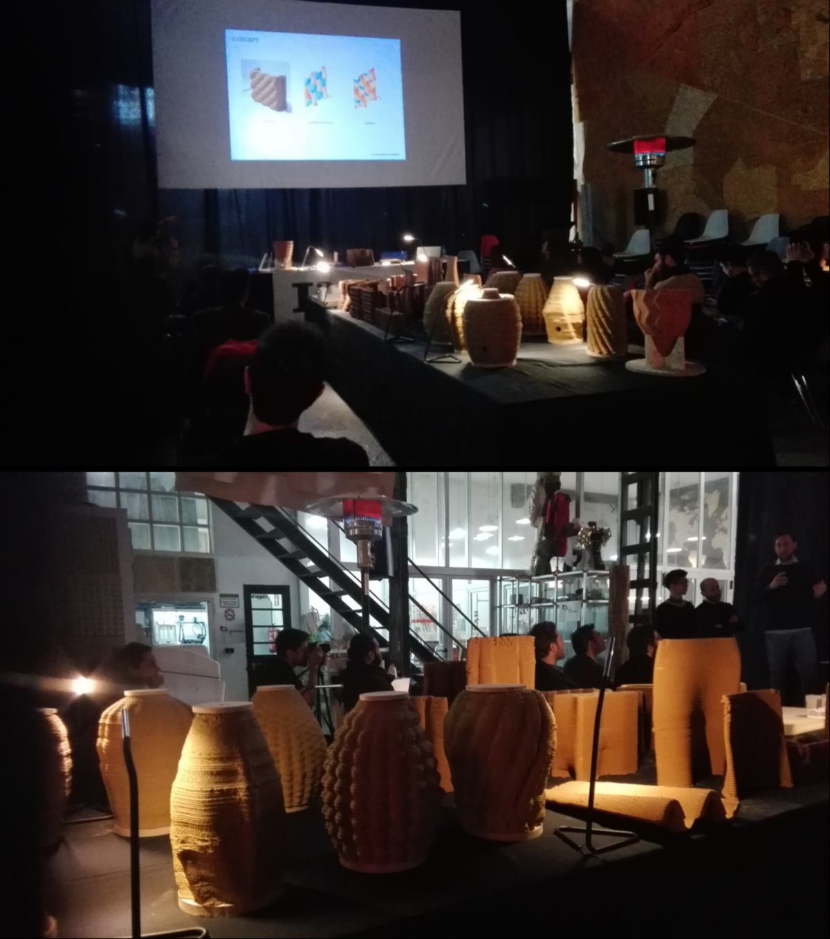
This is an excellent presentation about one of the advantage of 3D printing : the ability to design the internal structure of a material to confere specific capabilities, here thermoregulating ones. In practice, they designed bricks with pockets of air embeeded in it, and by varying the ventilation level and thickness, these bricks regulate the temperature inside buildings. The same change of inner structure also provides more support for beams or other horizontal structural components.
Adobe construction has been used for a long time, and 3d printing offers the ability to design with it with a much higher precision and, once set up, much less manpower. I am looking forward to see these technological improvements used in practice, expanding the use of a material that can be recycled many times over.
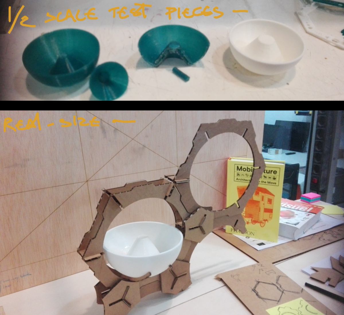
For now, I am reverting back to PLA to carry on with the prototype of the plant container. the reduced-scale prototype with added support has printed well but the water is not siphoned properly. I cut the model in half to diagnose the issue :
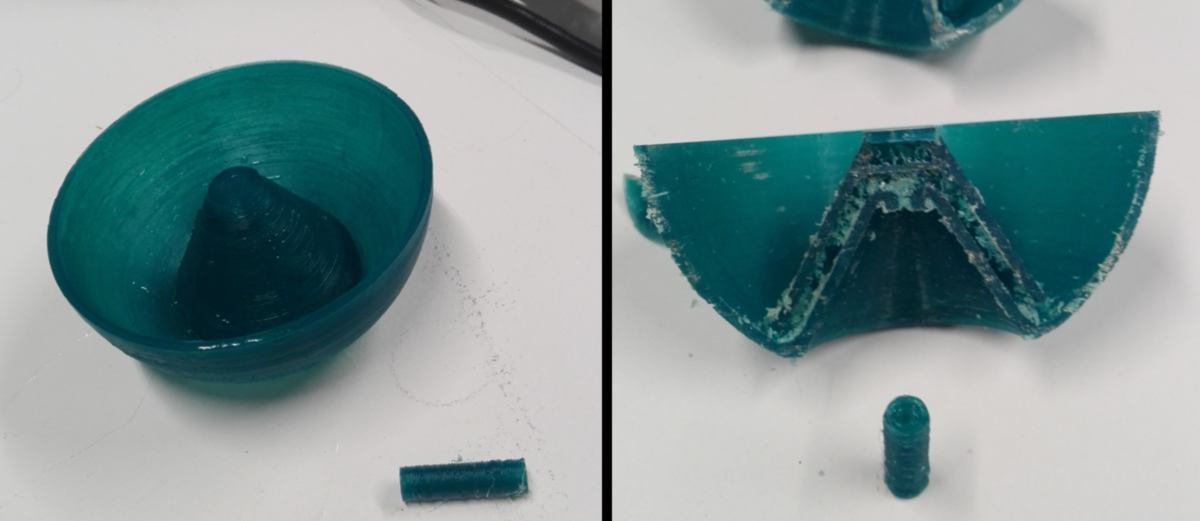
Due to the scale, the channels are cluttered with filaments, making it difficult for the water to flow. I adjust the design, making these inner channels as wide as they will be in the 1/1 scale model and send a new print :
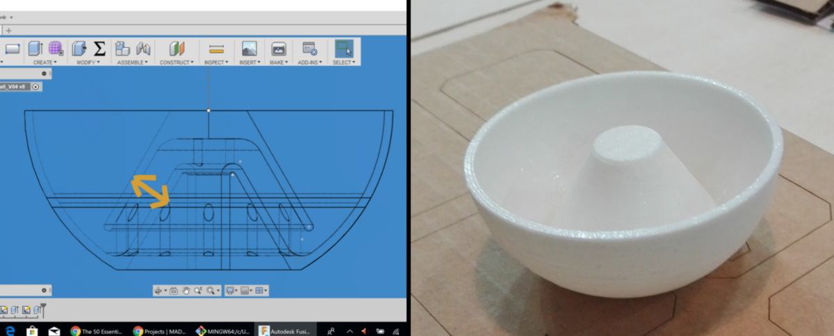
With this modification, the siphon system works properly, meaning that the siphon will work in the real-size model. Before I send it to print, I make a last addition to the design : an anti-splash system. The input of water will come from another container located right above it and will hit the container straight in the middle. For now, the middle is flat, therefore the water will spash everywhere, which will be messy and lead to water loss in the system. I find a bit of inspiration online and humbly design a first test :
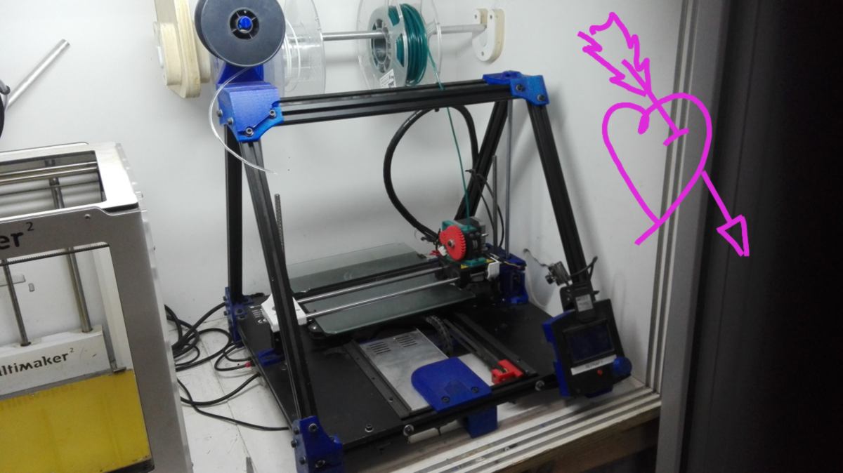
I want to acknoledge how resilient the 3d printer below has been over the last few weeks. I have learned how to manage filament switch, recalibration of the plate, basic network issues, and more. It does not take a $3000 printer to learn about 3d printing. The most important ingredient is to be nice to the technician in charge of it. Mikel has been incredibly patient, bearing with my many mistakes, thanks to him.
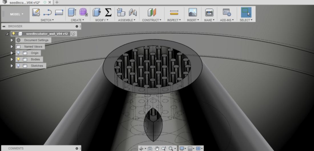
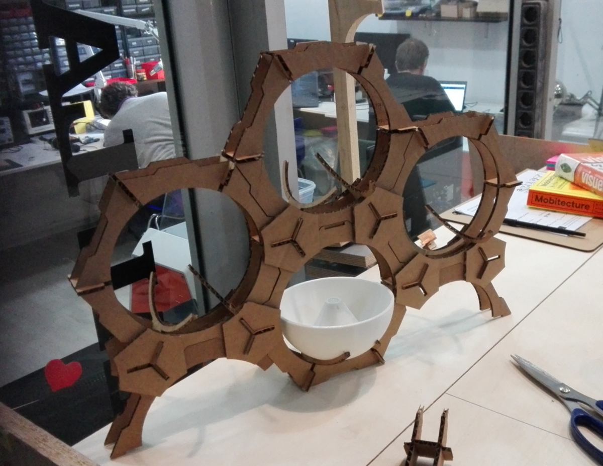
After many test-pieces I finally add a real-size 3d printed model to the cardboard wall :
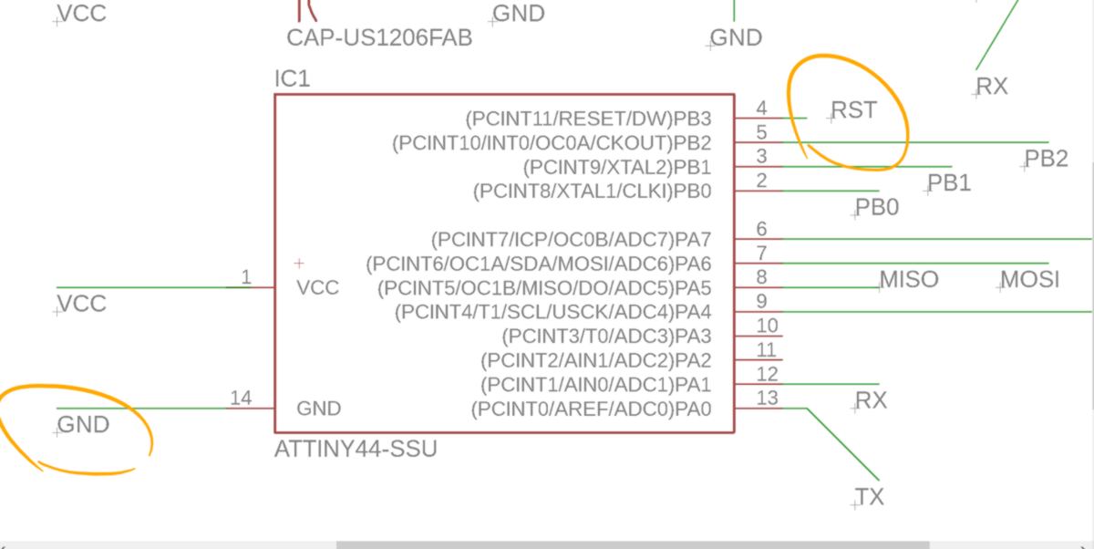
02.03.18 / Why Eagle? Naming a electronic software by the name of a bird of prey is a mystery to me. Existential questions aside, I begin the design of the board, supported by my tutors and other students.
It all begins at schematic level, where I select each component from the fab library downloaded from our lesson. I follow this tutorial ot import the new library. Rather than connecting them visually, which will result in a messy web of tangled lines, I label them appropriately to make connections :
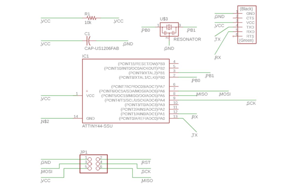
For now, my goal is merely to copy the board offered as an example. Once done, I switch to the board view, where all my element are at scale and connected by airwires. I need to turn these airwires into proper traces, which is usually a puzzle. I look for an automatisation of this task, which makes the job easier :
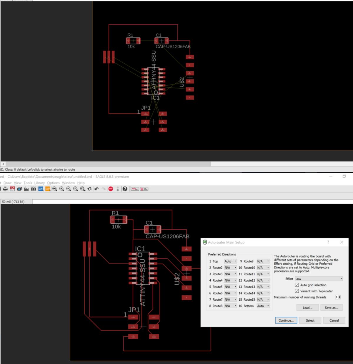
However, I realise after that that I had forgotten an element, and I have to use the maunal tools to re-trace the board. I also realise that I can optimise the traces by spinning around some elements.
I am being reminded of design rules about PCB, and defines the width of all traces and minimum clearance between them. Remembering the test piece we cut two weeks ago, I enter 16 mil, which is slightly larger than the width of our 1/64 cutting tool, as a basic value for all elements. I also discover the ability to add a grid adapted to these measurements:
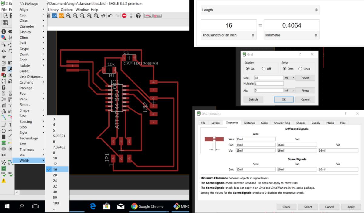
Later on, I will even switch to 20 mil to make the soldering stage easier.
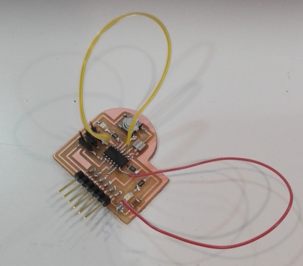
As a second step, I add additional elements to the board. Eagle enables me to switch back to the schematic view and add a switch, an LED and its resistor, as well as an extra LED + resistor bundle, which will light up when the board is powered :
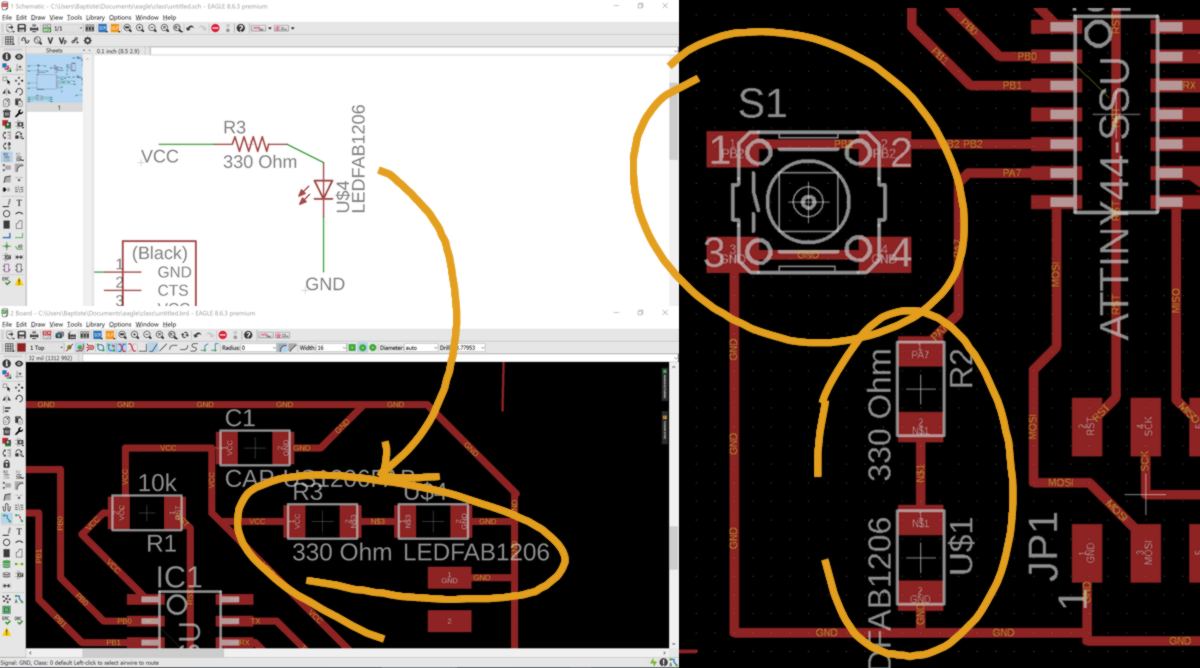
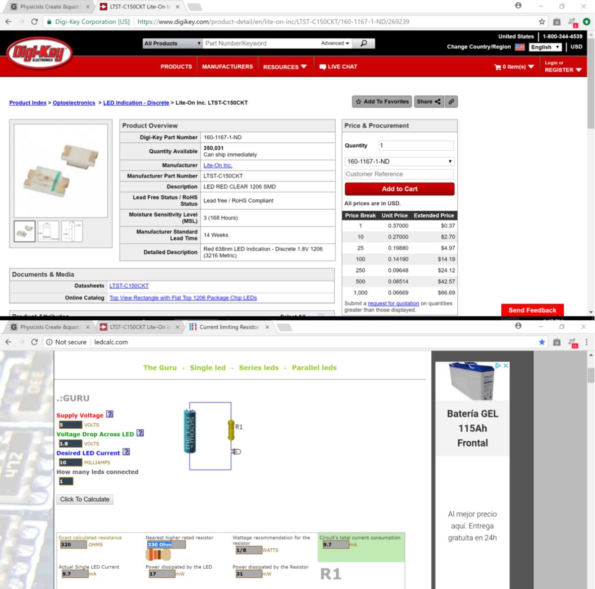
About the resistors, I calculate their resistance online, using the digi-key reference of the LED and a website offering a generic calculator based on Ohm's Law. It recommends the use of 330 ohms, but I know we do not have them here, so I will end up using resistors with 490 ohms, the closest value available, so as to not blow up my LEDs :
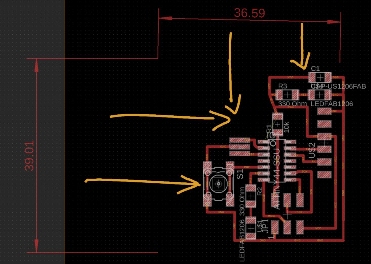
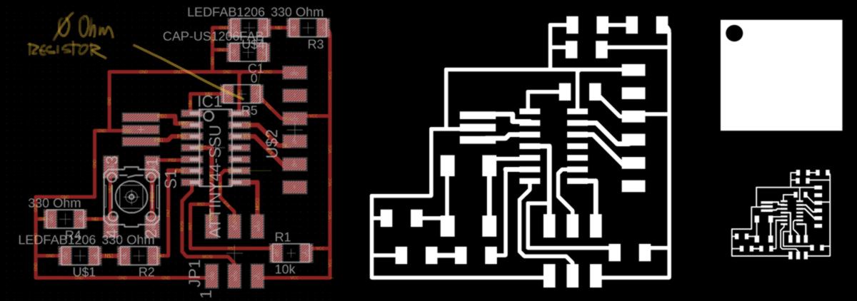
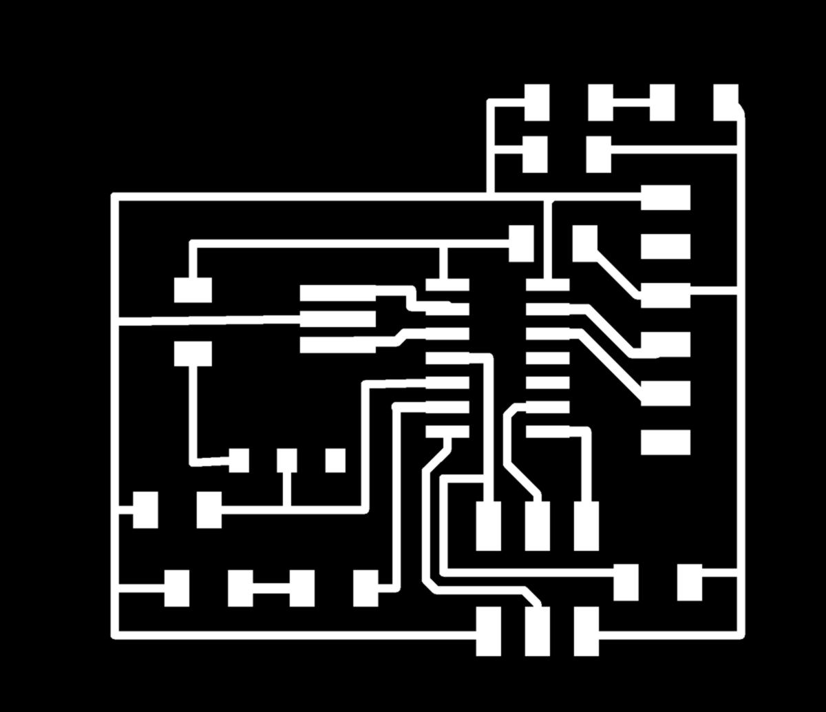
Before export I optimise the size of my board:
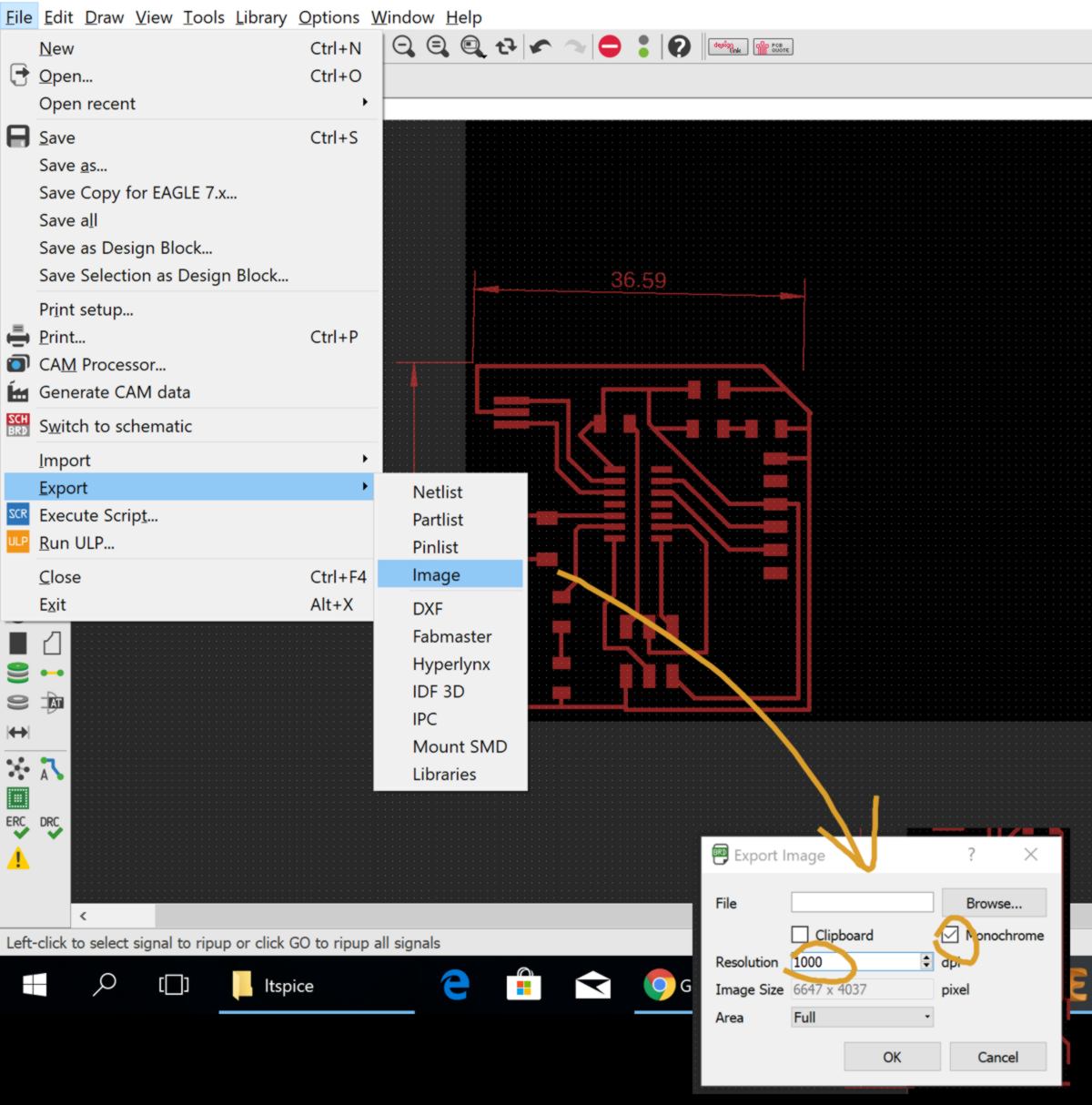
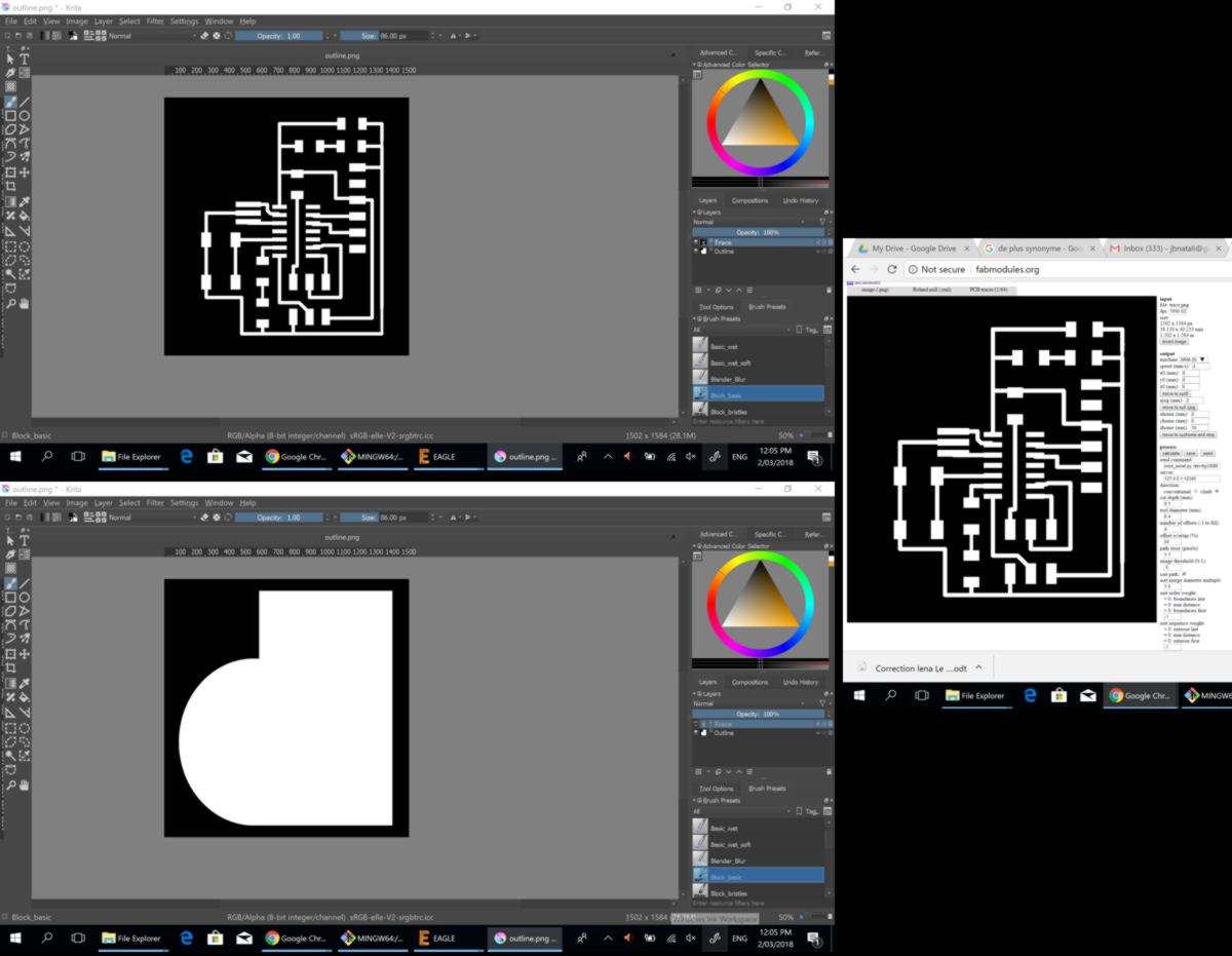
I can now export it as an image with a high resolution, selecting only the first layer where all traces are :
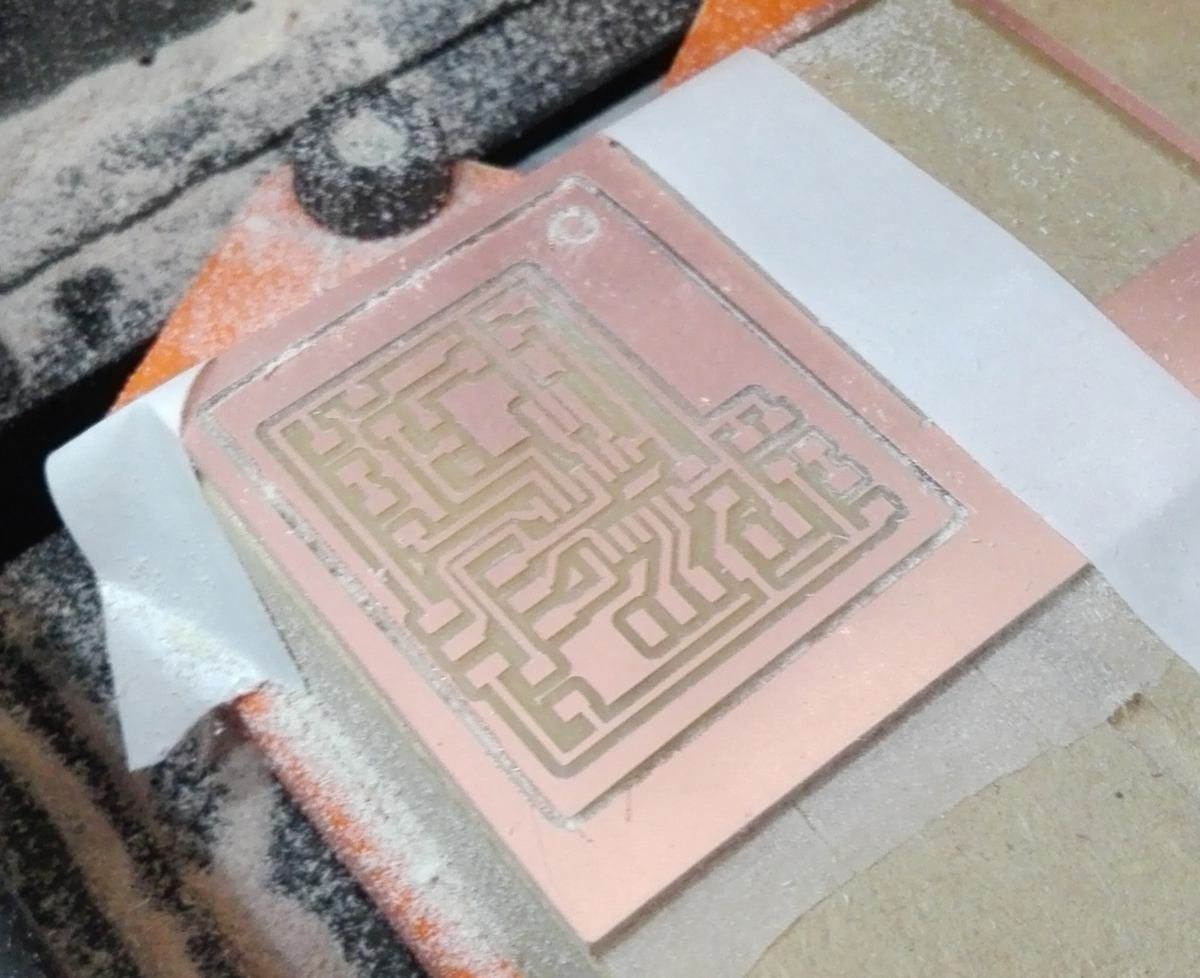
In Krita, I create an extra file based on the one I just exported. This file will be used to cut out the board. I will then use fabModules to generate the g-code required by the precision milling machine. It is identical to what we did one week ago :
I then, following the exact same workflow as two weeks ago, mill the pcb, collect and solder all components. One fun fact was that the 1/64 end mill at the very end of its cut, stayed stuck on my PCB, the machine heading back to it neutral position on its own. It somehow did not influence the quality of the cut, which actually went slightly through the board - our board are, as I discover today, thinner than the one set up by default in fabModules.
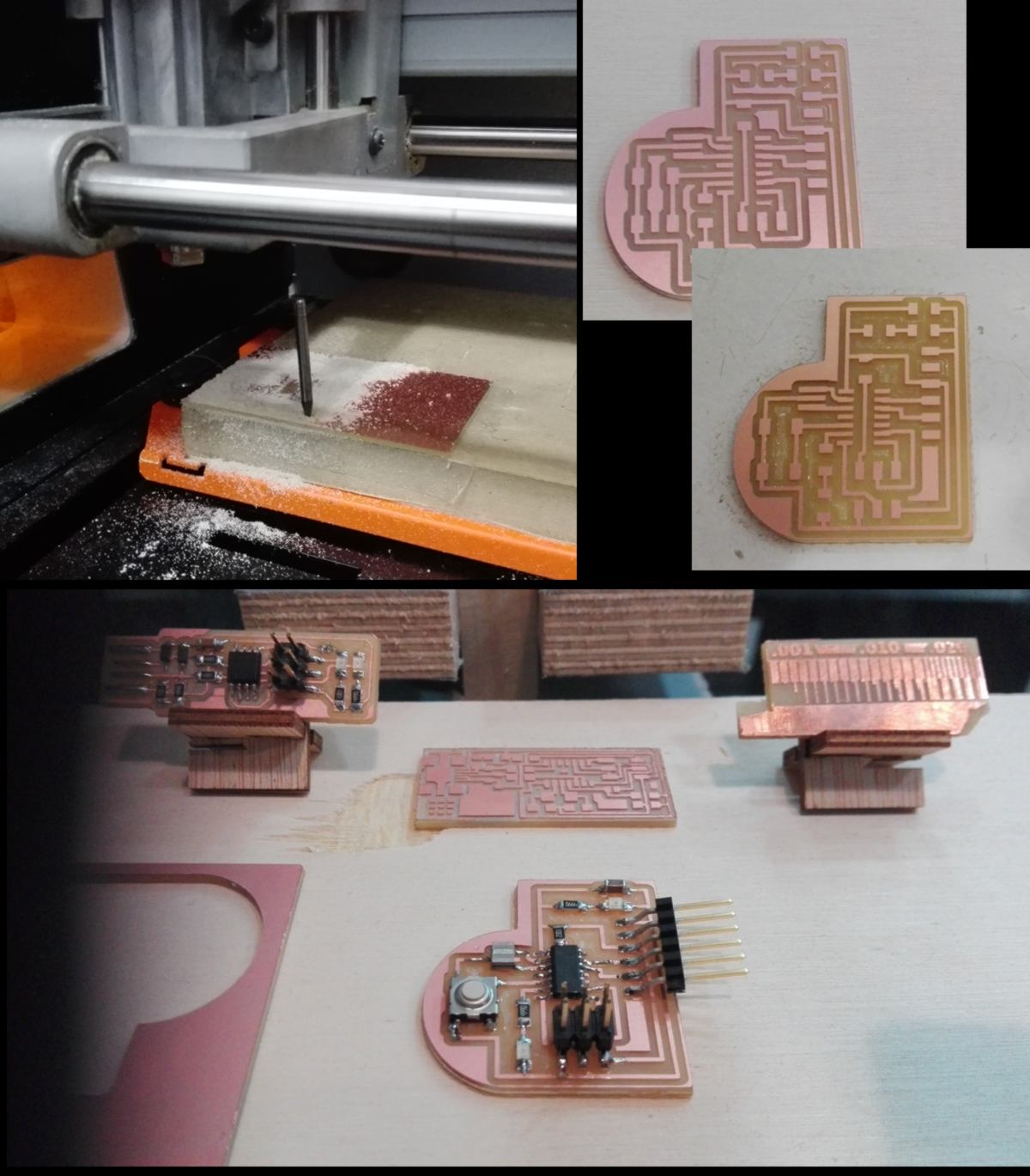
For now I will leave the board on my desk, waiting for next week to test it out.
05.03.18 / Testing the board from last week, I receive a few unexpected warning messages from the terminal. There will be a fair amount debugging today...
Arrived early, Andre and I have trouble finding a method with all ressources needed to test our board. We end up collecting different tutorials from former students and define our approach for today :
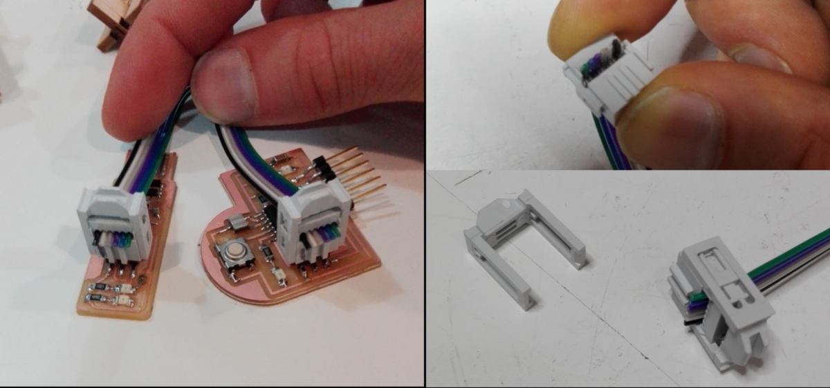
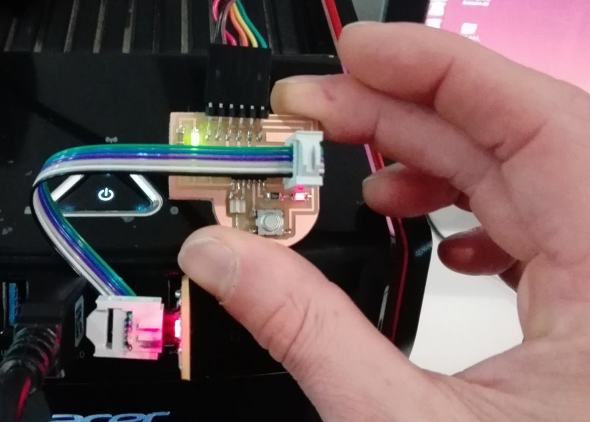
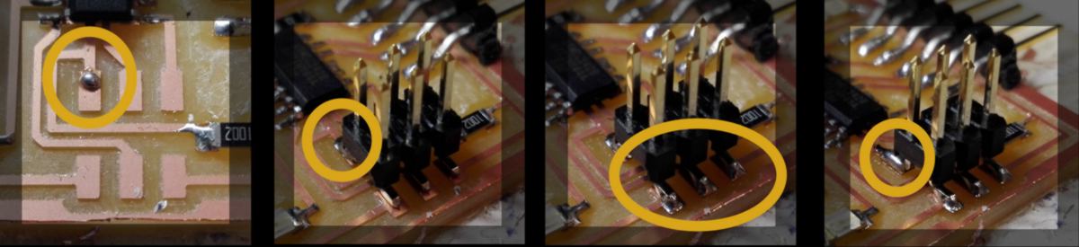
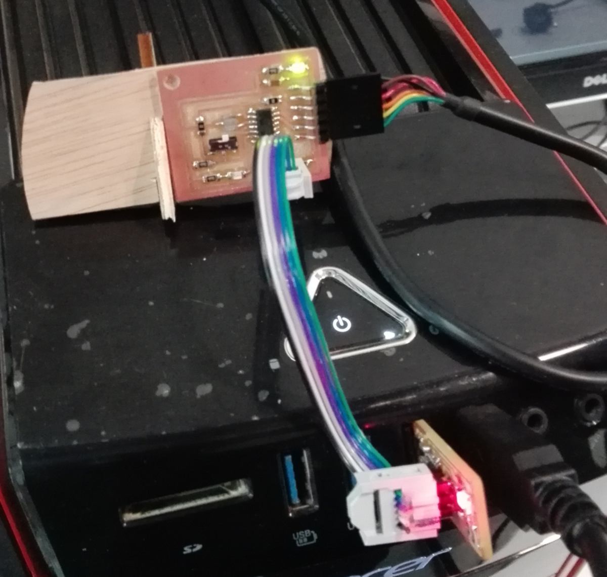
Firstly, to use the programers made two weeks ago, we put together a couple of cables for the ISP header. The uber-important aspect of this tiny fabrication is to remember where the ground is. Black cables are usually used as a guideline. I design mine with this in mind, also ensuring that the ground is located by the logo and name of the manufacturer :
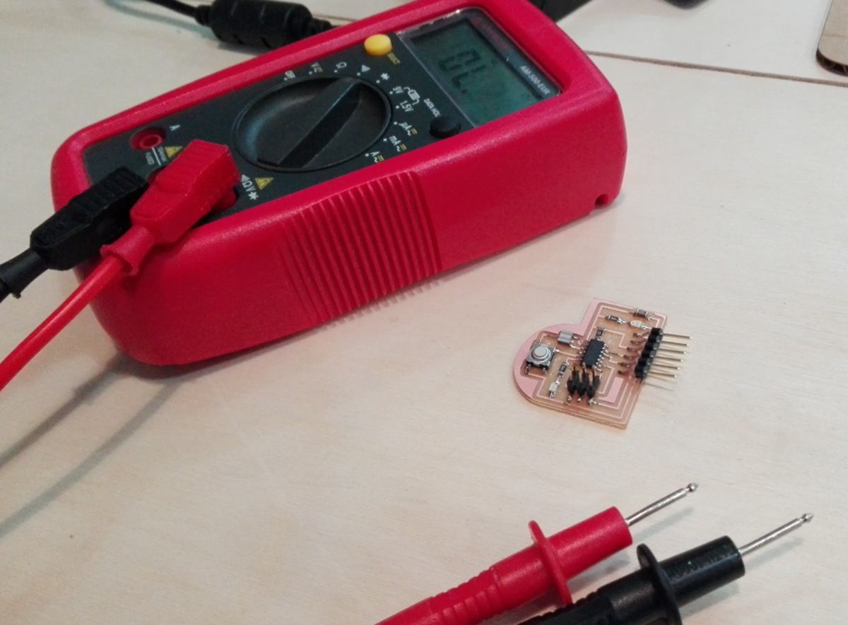
Secondly, I scan my board for short or open circuit using a multimeter. I cover all connections starting from the microprocesseur outwards, then move on to other components. I use the digital render of my board from Eagle as a reference :
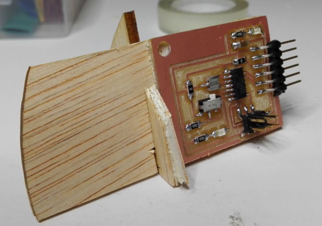
I then connect my programer and the board to the computer. Since I do not want to use my Wacom to do any programing, I will switch computers a few times today, experiencing both Linux and Mac environment. The extra LED that I added to the design lights up, providing me feedback. The board is correctly powered :
I know begin to go through the following commands, having loaded the three files required :
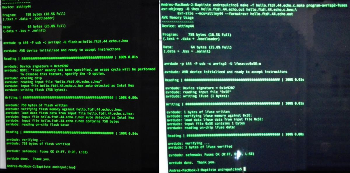
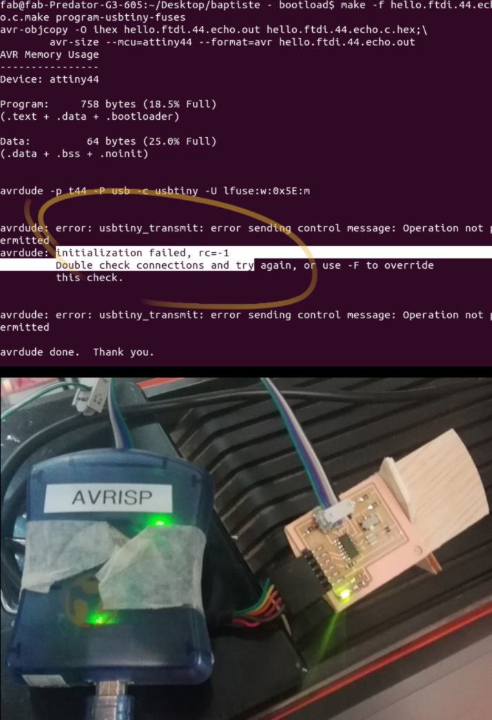
I first double check that both boards are detected by the computer, then begin to enter the command lines. At the second stage, I happen to get a warning :
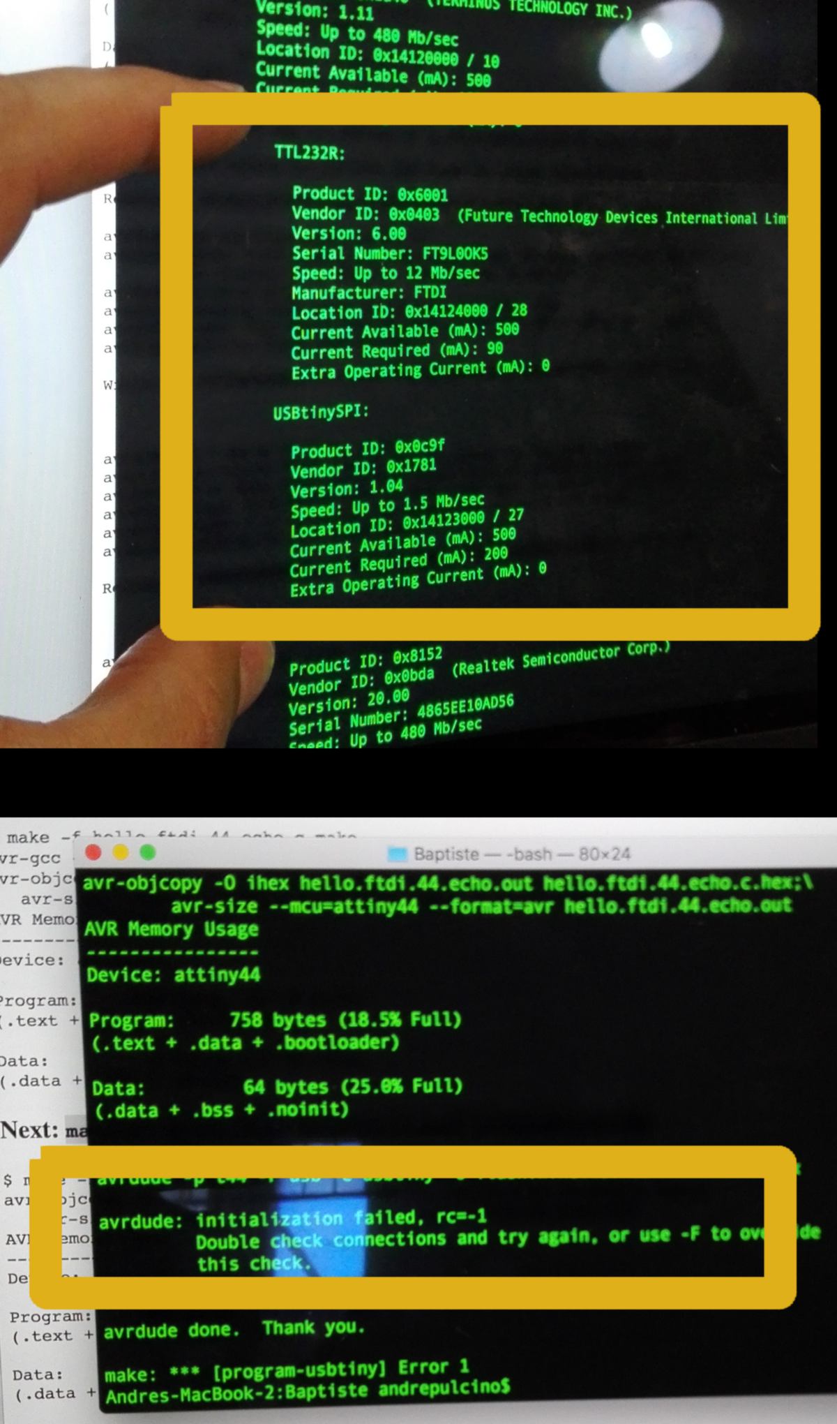
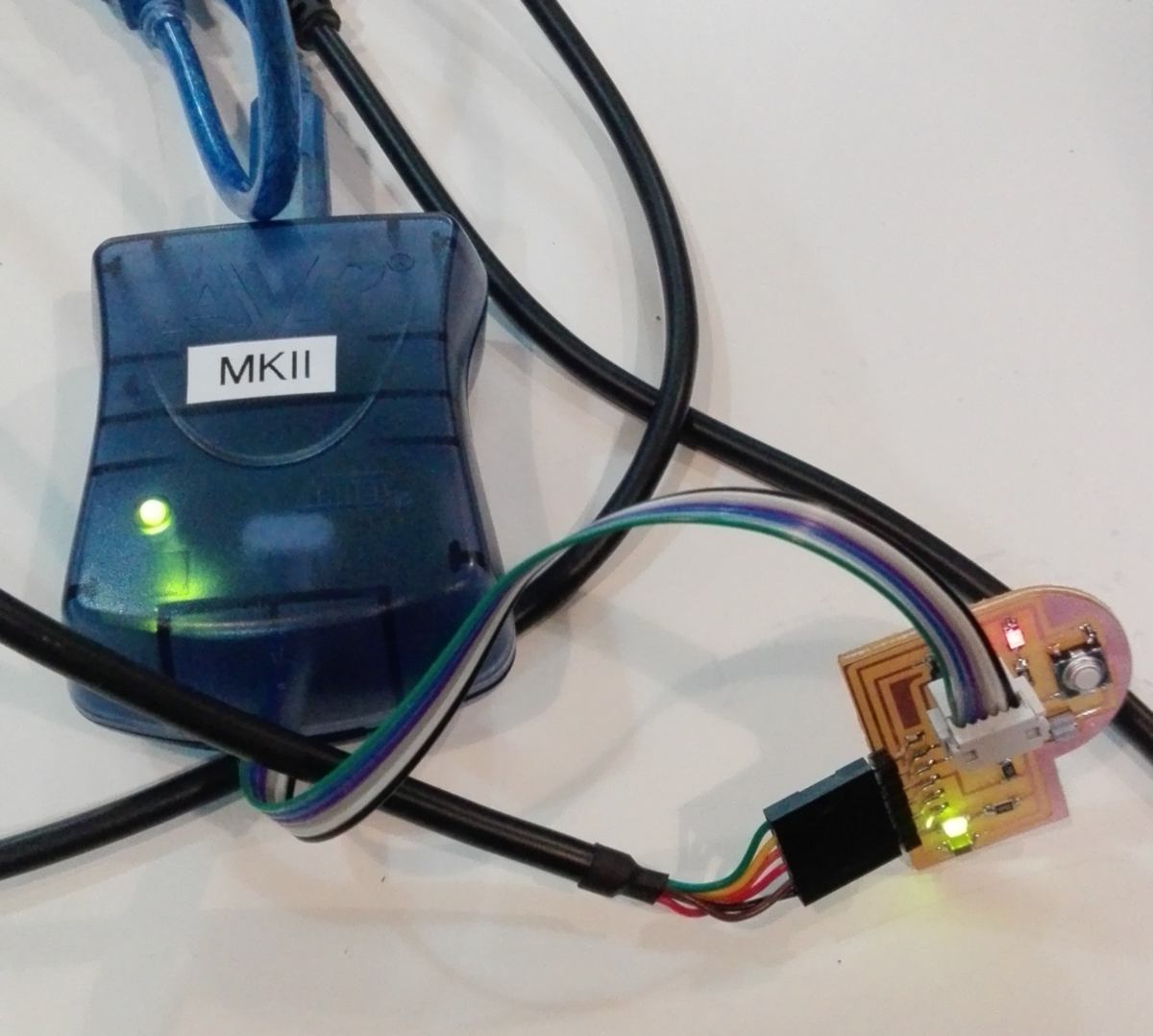
To verify that the problem comes from my board, I use another programer and repeat the process. This implies modifying the command lines slightly to trigger programs adapted to the new programer, here an avrisp2 :
I end up with the same warning. After considering different options, I head back to the schematic of my board and compare it with the Hello board provided by Neil. I am stunned by the blatantness of the mistakes : when wiring my board in the schematic, I have missed two connections :
It gives me the opportunity to craft some airwires, tinning and soldering a couple of connections to connect these different points and finish my test :
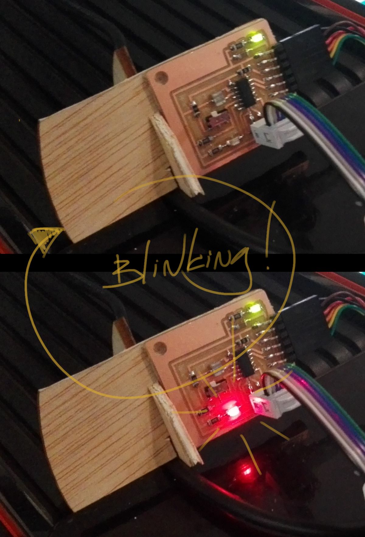
I then test the board out again, this time flashing the board successfuly :
I must re-design my board tomorrow. This mistake has given me an idea to alter my design and add some fun to it. This week, we will also begin to use the CNC machine, therefore I work on the green wall system, laser cutting a few more modules to have a better idea of what it will require. This time, I order my cut so pieces at the centre are cut before the outer pieces, and so on :
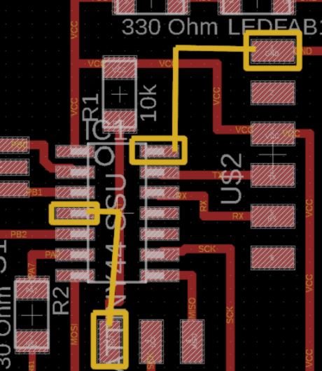
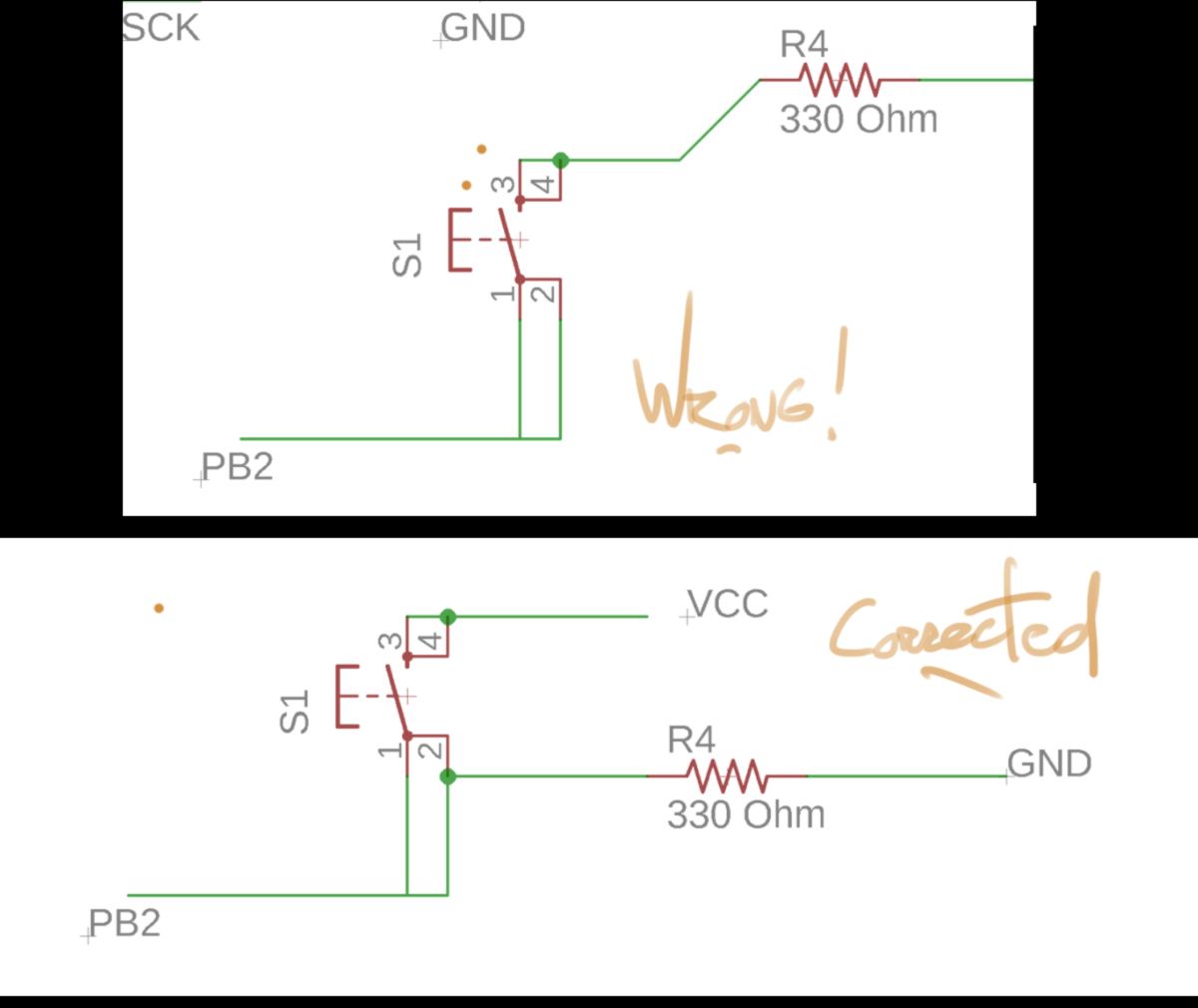
06.03.18 / A few corrections in my electronic design are required after yesterday's findings. To begin with I add the missing connections in my schematic drawing :
I then add an extra resistor to the switch (A), under recommendation of my tutors. Accessing the VCC of the microprocessor has become quite difficut so I also add a 0 Ohm resistor to allow the VCC trace to jump over another one (B):
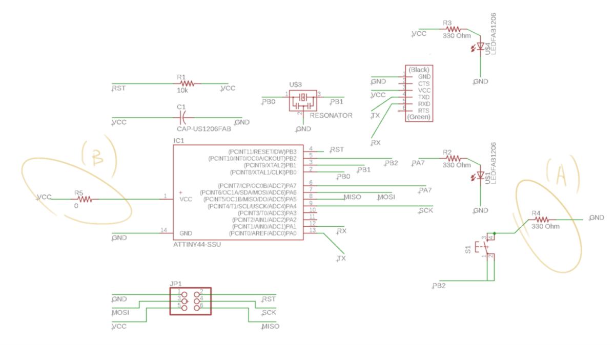
this is how the corrected design look like :
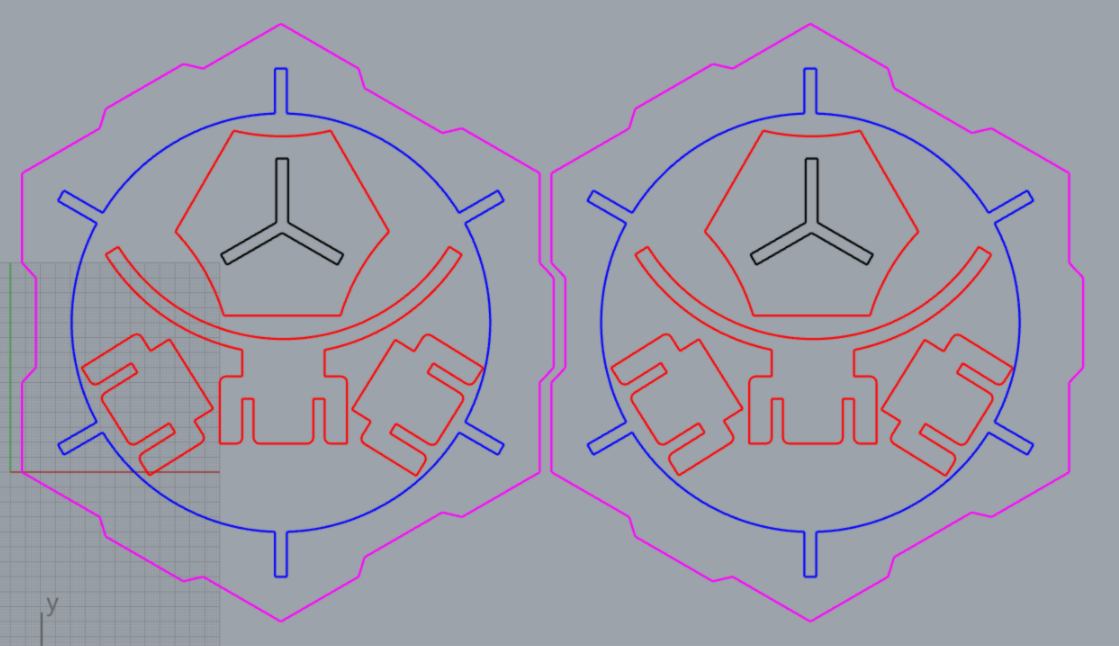
The CNC week approaching fast, I begin to prototype the base of the green wall, containing a receptacle for the water and fish. I test two different type of support, varying shapes to find the one offering best resistance to vertical and horizontal forces:
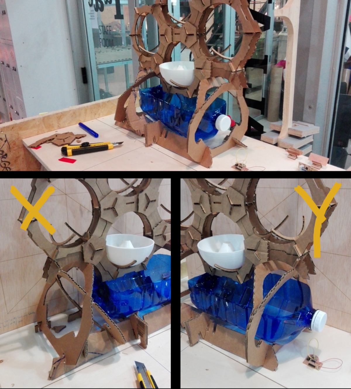
As aesthetic as the Y shape is, the X shape is superior, offering resistance in both directions.
I take this last evening before class to go through all links put online by our tutors. I find the sparkfun website very useful, and some important exercises are described by former students to better understand dynamics and power.
More importantly, I get to understand what are the implications of the way my switch and its resistance are set up, thanks to Steven Chew :
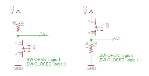
My set up falls under the second case, therefore I must carefully follow the logic dictated by this setup for future programming.
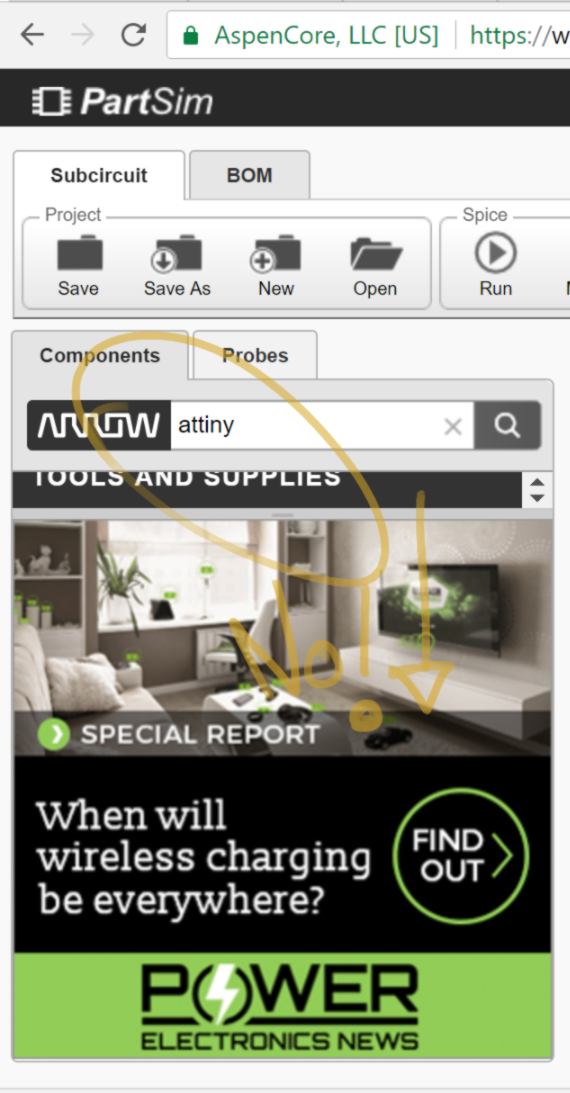
Looking for another method to simulate my board, I look at partsim . The design of the online tool is really sharp but the location of the advertisement makes it impossible for me to use the drop down menu :
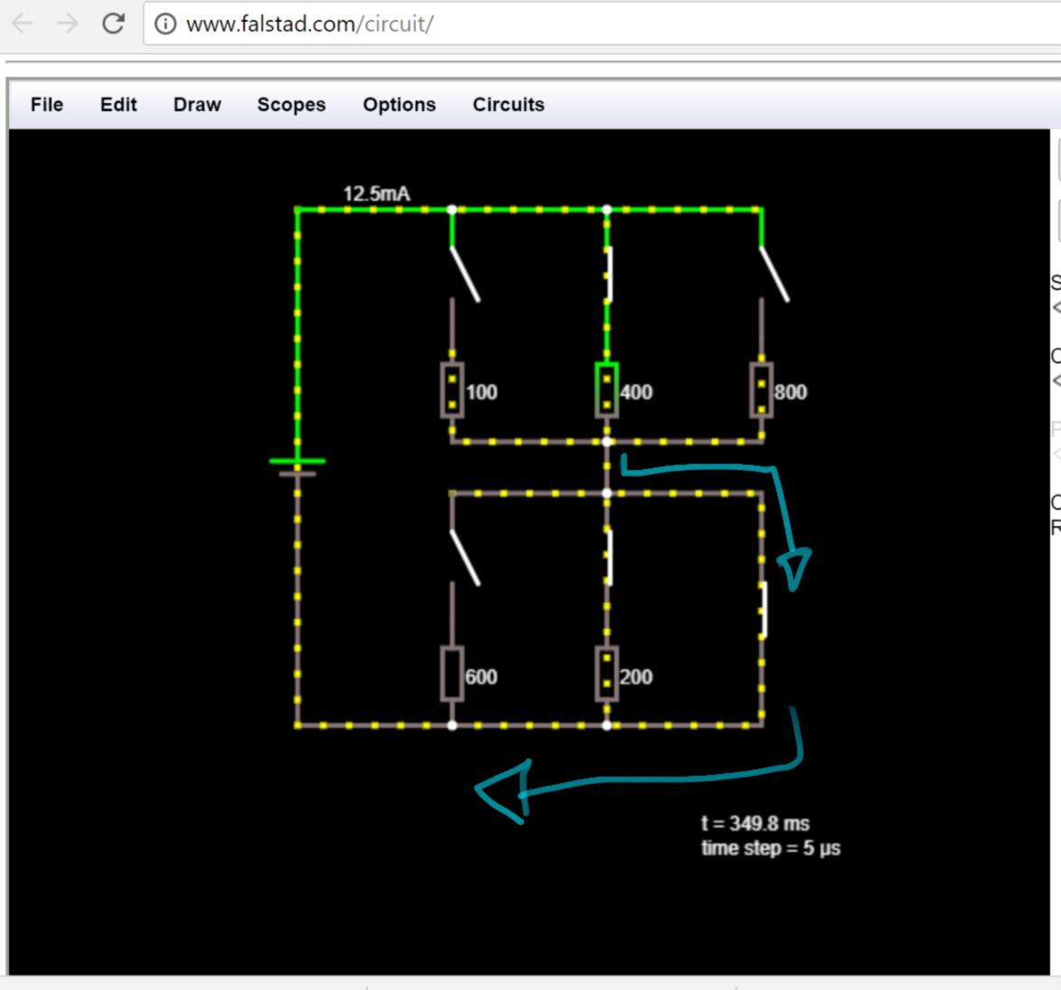
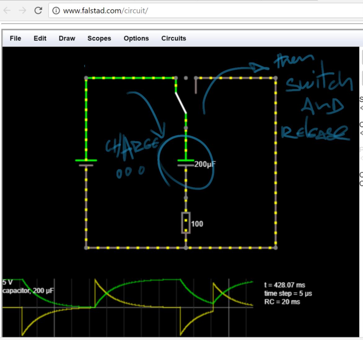
Looking at falstad , I learn a lot about how electricity reacts with visual feedbacks. I get to understand how electricity takes the path of least resistance, how a capacitor stores, then release electricity, and more basic concepts :
I do not grasp many schematics so I start reading a somehow concise guide of electronics , looking for some general knowledge and concepts which will make my life easier down the line.
07.03.18 / I go to Tinkercad to simulate my board. I replicate part of the board using similar components, then write some code to make the LED blinks when the slideswitch is switched on :
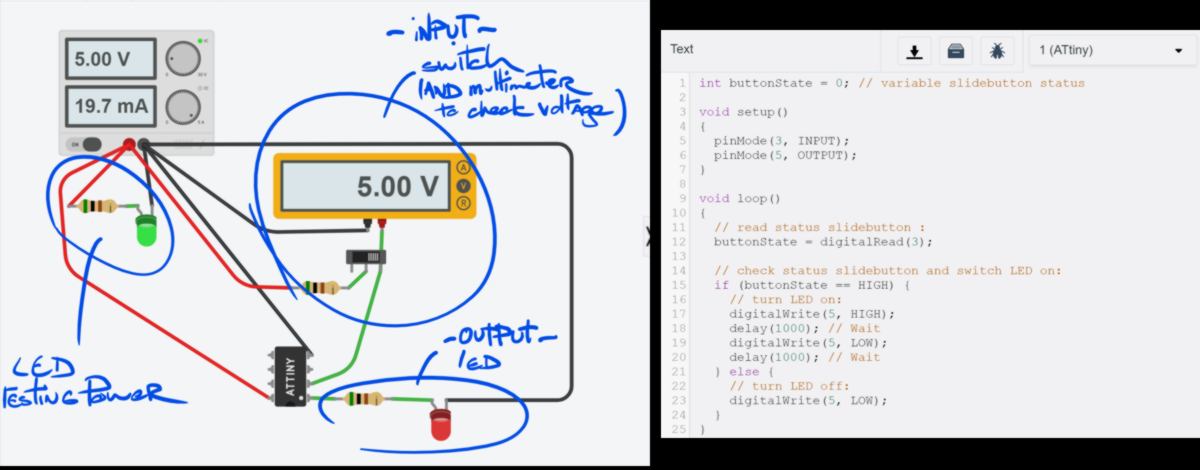
In this case, the multimeter acts as an extra connexion. Once I take it off, the pin does not receive any input anymore. After a few tests, I get to understand that my understanding of how the Pin acts in this system was wrong : the PIN does not receive any power, and is not part of the "circuit". The Pin only "listens" to a circuit and determine whether it is High or Low. A correct circuit should look like this:
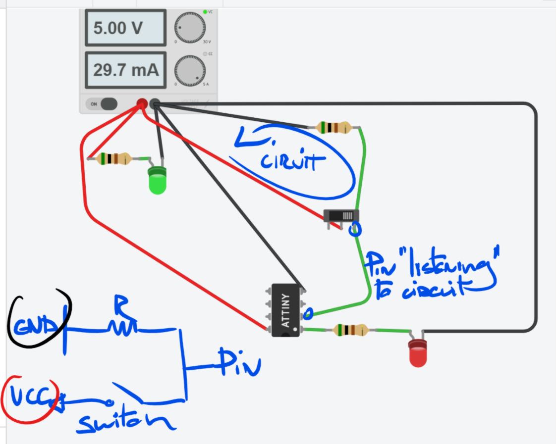
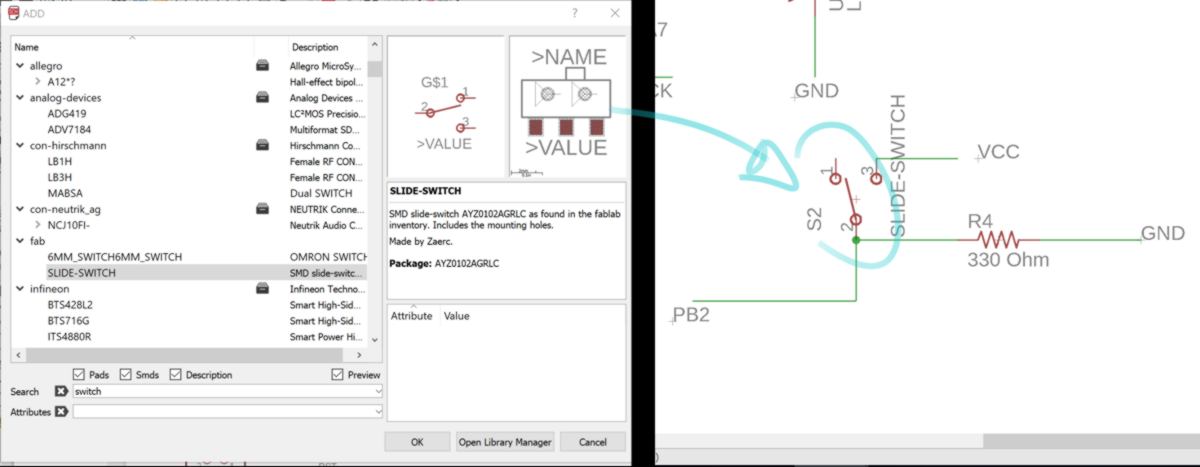
I redesign my board accordingly. In the process, I swap the pushbutton for a slide button :
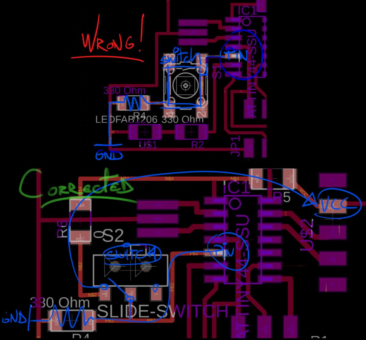
this is how the corrected design look like :
08.03.18 / I am back in the soldering room, Cutting and stuffing my board. I now know the location of each component by heart and solder without needing the schematic. As a side note, I finally designed a very basic workflow to solder more efficiently :
This board must be bootloaded. This time, I do this task myself entirely. Using the lab computer, I plug my new board to my isp programmer :
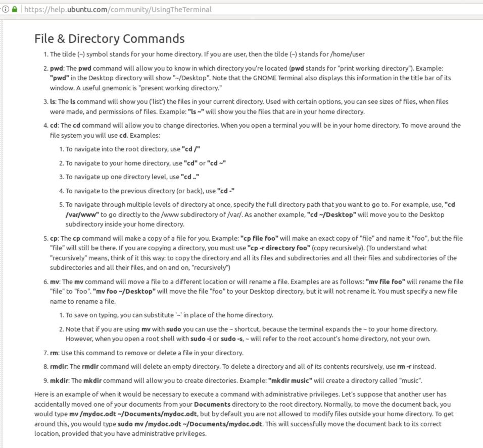
I will programm the board using command lines in a Ubuntu environment. I collect some basic programming knowledge to send commands such as folder selection and more on the ubuntu official documentation:
As I did yesterday, I collect two compulsory working files and a method to assist me in the process on the description of the embeeded programming schedule :
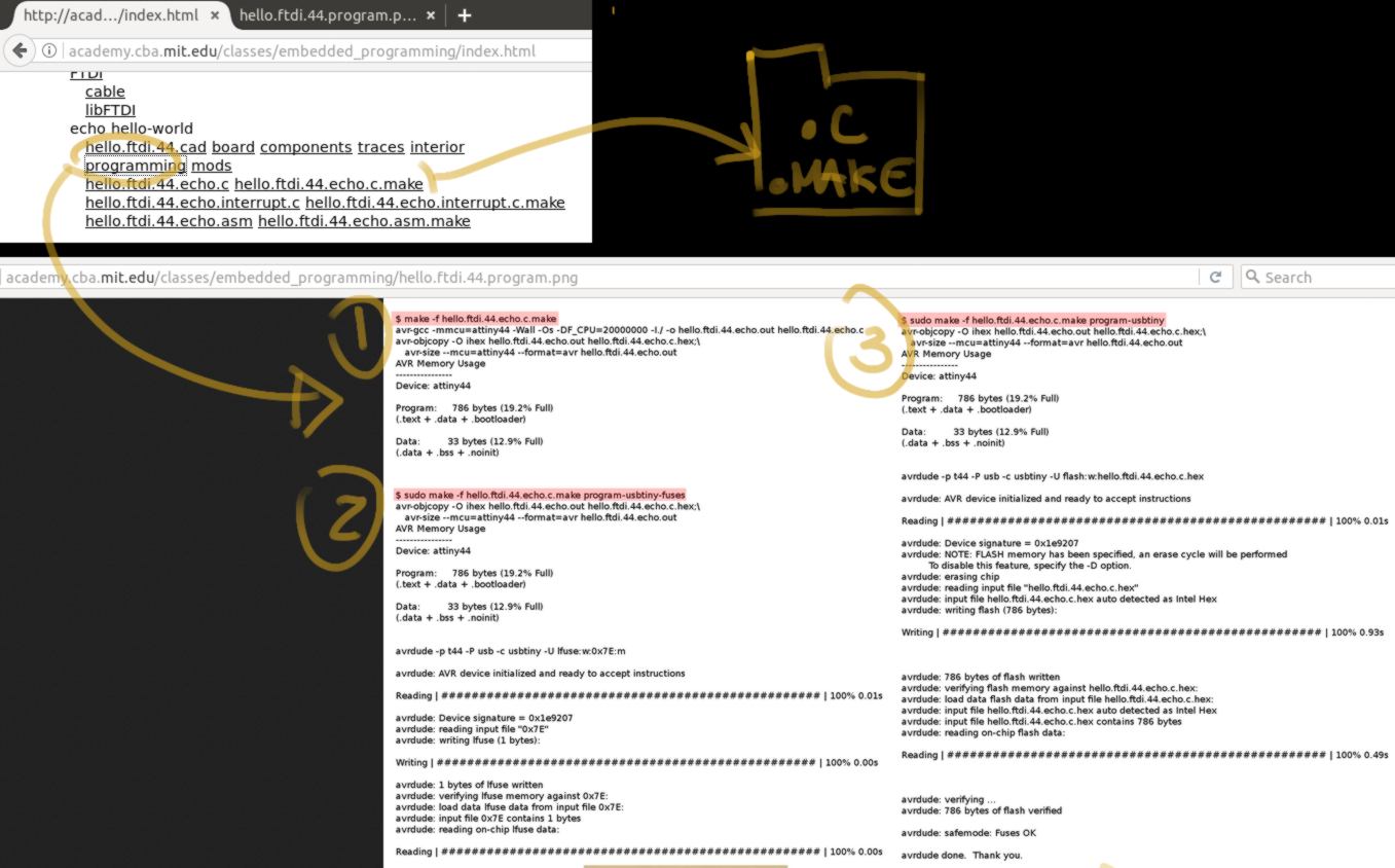
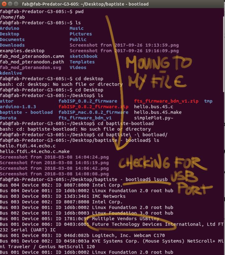
From the terminal, I position myself in the folder where the files have been downloaded and check that both the ISP programmer and my board are detected :
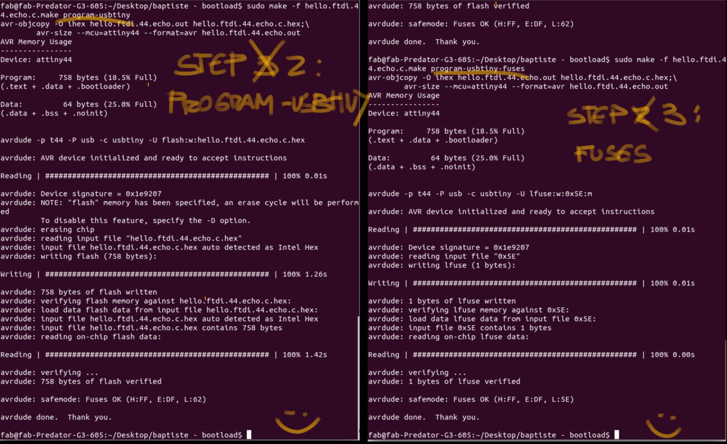
I go through the steps required. At the second step, I get an error message, warning me about an initialisation issue. To verify that my board is correctly wired, I connect the manufactured ISP programmer, which return a green - positive - feedback. The issue lies elsewhere.
I remember that a few days before, going through the same steps, we sent the "fuses" command after the "usbtiny" command. I swap these two steps and get positive feedback, finishing the bootloading from my isp programmer:
I wish to go one step further, programming this board in a similar way as the simulation I ran yesterday. To do so, I need to load a library for the arduino IDE. A website called high low tech describes this process accurately. The first step is to target a board library which enables the Arduino IDE to communicate with the Attiny44 :
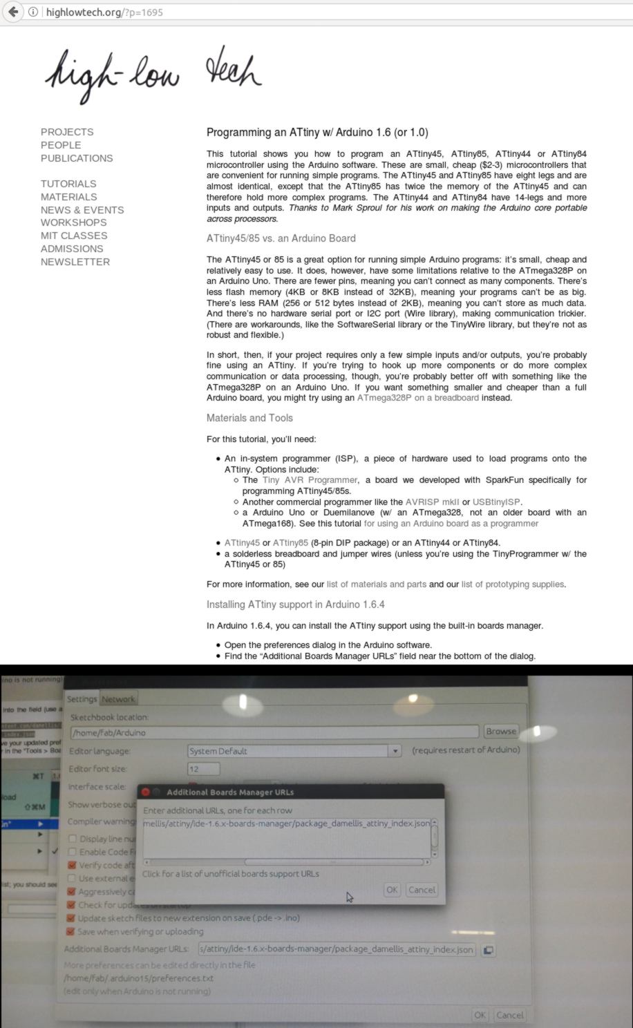
I then install both the library and board manager for the Attiny :
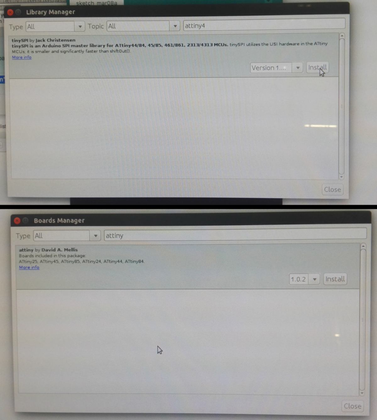
I then specify the type of board (the Attiny24/44/84 is now available in the list), specific microprocessor, clock and finally programer used :
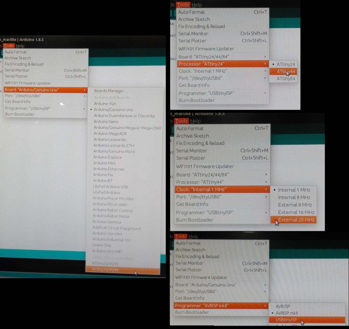
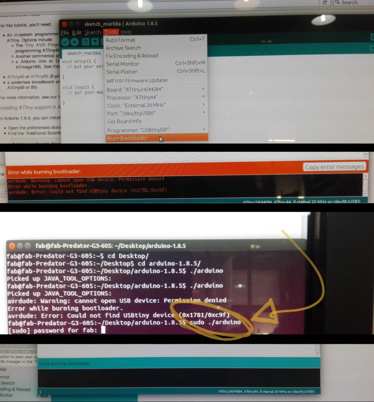
The last stage( not compulsory in my case since I have just bootloaded my board, but still relevant for testing purpose) is to burn the bootloader to initiate connection. I get an error message, then rectify it by closing and restarting the Arduino software in administrator mode, using the right command line. The board is now ready to be programed.
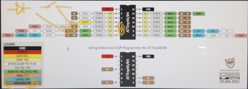
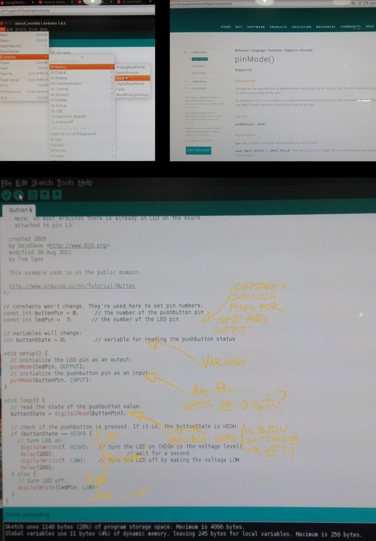
The Attiny44 and the arduino board have corresponding pin schematic. Here, my slideswitch and LED are located on pin 5 and 6 of my attiny44 respectively. In the arduino IDE, I will use their corresponding pin number, 8 and 7 respectively :
Using both the help section of the arduino website and examples readily available with the software, I write some code to make the LED blink when my switch is on :
By debugging my board again and again, I got to better understand interactions between components, basic principles about electronics, and got humbly introduced to programming.
19.06.18 / LAST MINUTE ADDITION I will go through the basic tools I use in Eagle as well as describe how I use the multimeter.
I use a very little number of tools in Eagle :
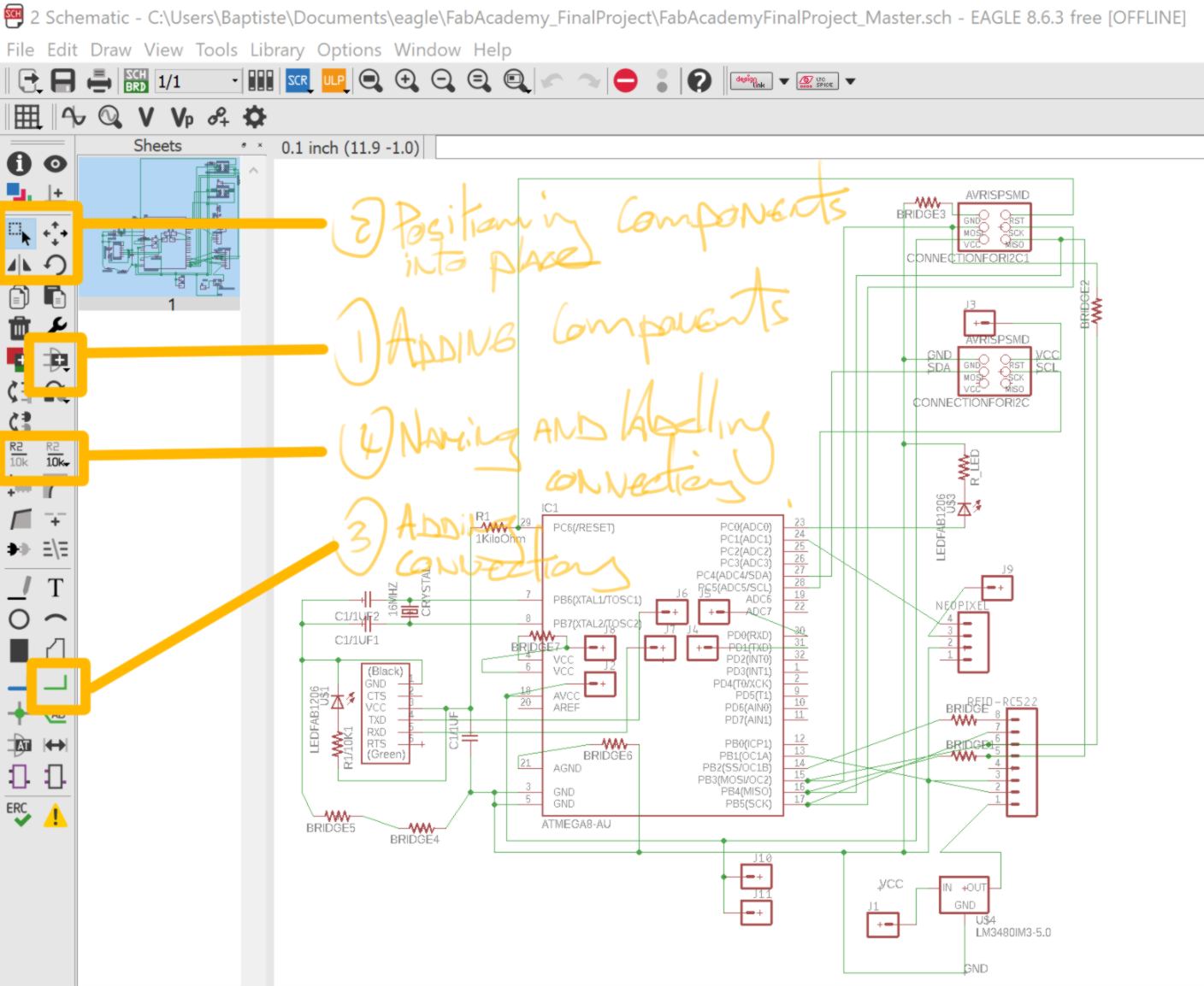
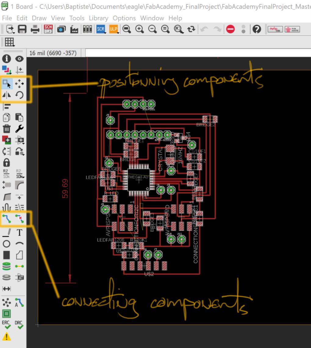
In the "board" layout, I often change the type of tracing used by right-clicking. 90 degrees-angled traces tend to be cut neatly, therefore only only switch to traces cut diagonally if forced to.
The multimeter I commonly use at the lab is a DT830B :
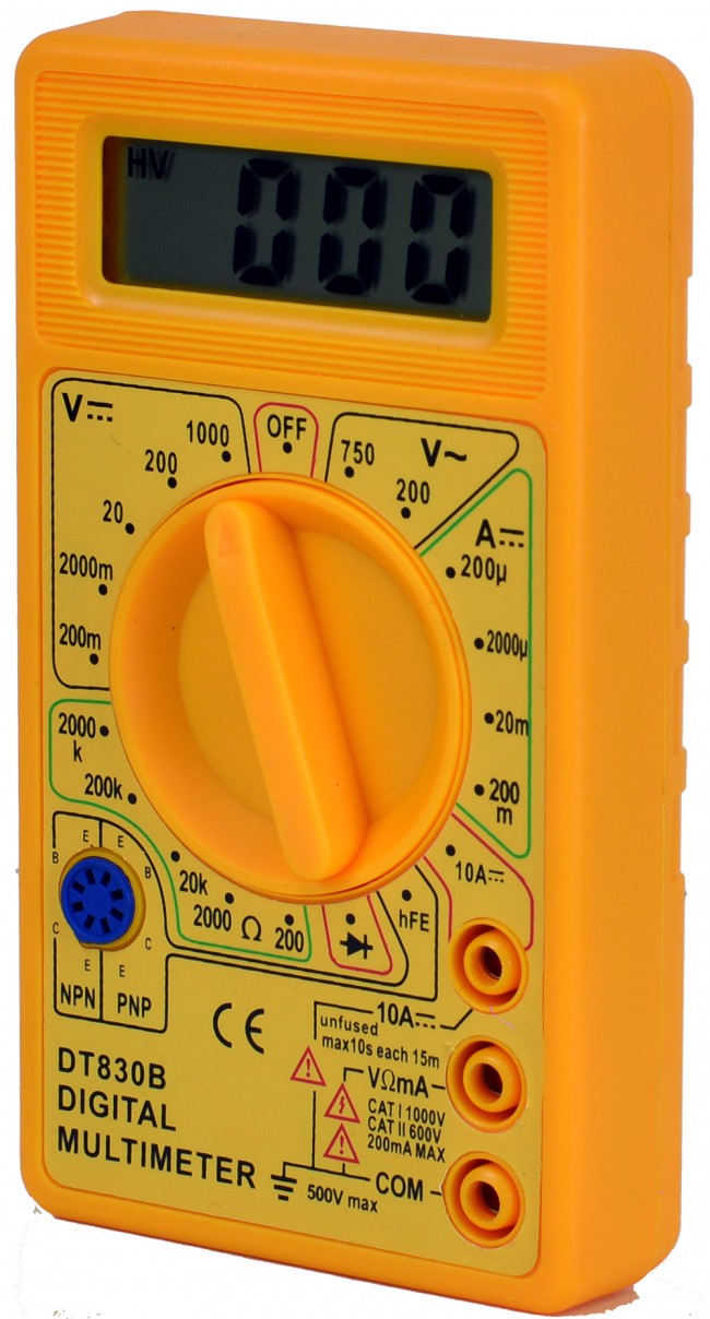
I mostly use it to detect short circuit or unwanted connections between traces/pins, relying on the continuity measurement :
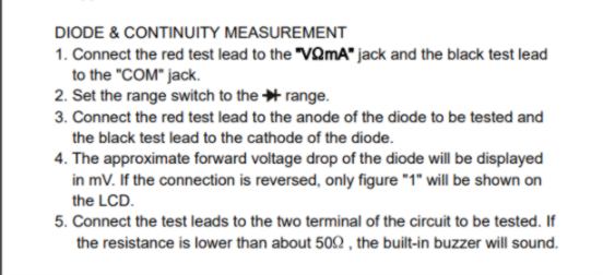
This tools offers many other features, able to measure DC/AC current, voltage, resistance and more as described in the datasheet (linked above).