Attending the Fab Academy in Barcelona, I document each week of intense learning as I come across new digital fabrication techniques.
This documentation is as much a report of what I do as a reflection on why I do so, and will hopefully guide me back to Oceania to spread and make good use of the knowledge gathered along the path.
--- summary of the assignment ---
objective :
Read a microcontroller data sheet. Program your board to do something, with as many different programming languages and programming environments as possible. Optionally, experiment with other architectures.
what I did :
Since I have previously programmed my board, I focused on reading the datasheet thoroughly, attempting to decipher the most cryptic parts.
Learning outcomes :
07.04.18 / I begin this week by reading an article posted by Oscar , another fab Academy students who is more advanced in electronics tha most of us. He has written an article about the ISP programer and bootloading the ATtiny44.

I get a description of what the following are:
I go through tutorials such as this one recommended by Oscar.
I now understand the use of :
I move on to the ATtiny datasheet . It looks like a long read so I make myself comfortable :

--- Introduction to the ATtiny world ---
All ports PA and PB types are bi-directional, either 4bits or 8 bits. This reminds me of a class with Guillem providing us with an insight about how to speak to a microcontrolller in C to tell which switches are high and which are low in an 8-bit system.
I then come across a diagram of the whole chip. Again I recognise some terms :

I look up the term Register : " temporary storage locations inside the CPU that hold data and addresses." There are 32 general purpose working registers containing a sub-set of 6 registers with an added function : indirect addressing.
I understand that according to the model used, the memory ( or memories : Flash, EEPROM and SRAM) will vary. The microprocessor has a stand by and sleep mode, running only the oscillator to lower power consumption.
I aslo mentionned a touch sensor system ready for use, directly implemented in the chip.
First comes an overview of the Central Processing Unit (CPU) core, which looks after program execution. To do so the CPU "access memories, perform calculations, control peripherals, and handle interrupts". As expected many technical descriptions are cryptic to me at this stage. However I learn that :
Within a single clock cycle, data can be fetched, operations executed , and result stored :

I stopped my line-per-line reading to get an overview of the overall document. I see that technical explanations are given, followed by example of code in Assembly and C.
--- Clock system - how the ATtiny defines time ---
I go through the Clock systems (CPU, IO, Flash and ADC clocks). A Clock source is determined by Flash Fuse (any connection with the Make Fuse command?) amongst these possibilities : External Clock, Calibrated Internal 8 MHz Oscillator (the chip has its own pre-built oscillators), Internal 128 kHz Oscillator, Low-Frequency Crystal Oscillator, Crystal Oscillator and Ceramic Resonator, the one I set up on my ISP and board.
Every time measurement is counted by clock cycle. As it appears : "The speed of a computer processor, or CPU, is determined by the clock cycle, which is the amount of time between two pulses of an oscillator. Generally speaking, the higher number of pulses per second, the faster the computer processor will be able to process information. The clock speed is measured in Hz, typically either megahertz (MHz) or gigahertz (GHz). For example, a 4 GHz processor performs 4,000,000,000 clock cycles per second."
If I understand correctly, The ATtiny 44 can only execute one instruction per clock cycle, but since the clock source set up was a 20Mhz Ceramic Resonator, a conversion tells me that 20.000.000 cycles per second will occur.
A description of how to calibrate internal clocks is given. Interestingly a low power oscillator is available (128Khz). The speed of the system clock can be divided ( by a power of two) to fit requirement of some applications using the system clock prescaler.
--- Power Management - how to put the ATtiny to sleep ---
The ATtiny has been designed to use low power if required, offering sleep modes which shut down modules in the CPU :
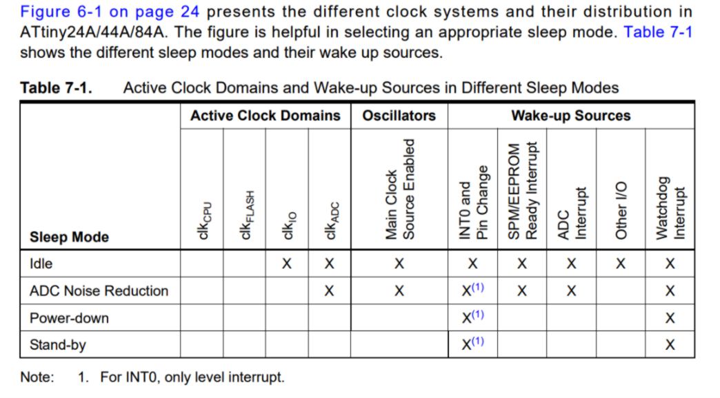
There are three of them, switching off more or less modules and " the contents of the Register File and SRAM are unaltered when the device wakes up from sleep". The two modes that use less power differ in the way that one keeps external oscillator running while the other disable it.
--- Resetting the AVR ---
All I/O Registers can be reset to their initial values, and the program restarted. There are different sources of reset possible.
I briefly cover Internal voltage Reference, Watchdog timer and Interrupt to get to what I am particularly interest in for the Input week : I/O ports.
08.04.18 /I carry on my reading :
--- I/O Port - getting a conversation going ---
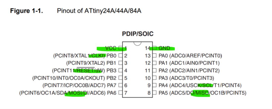
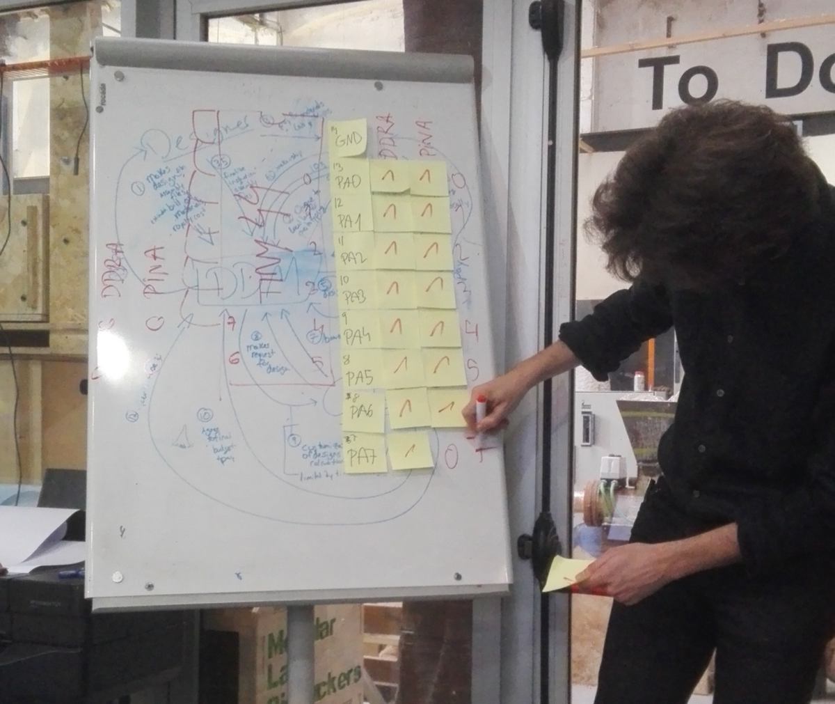
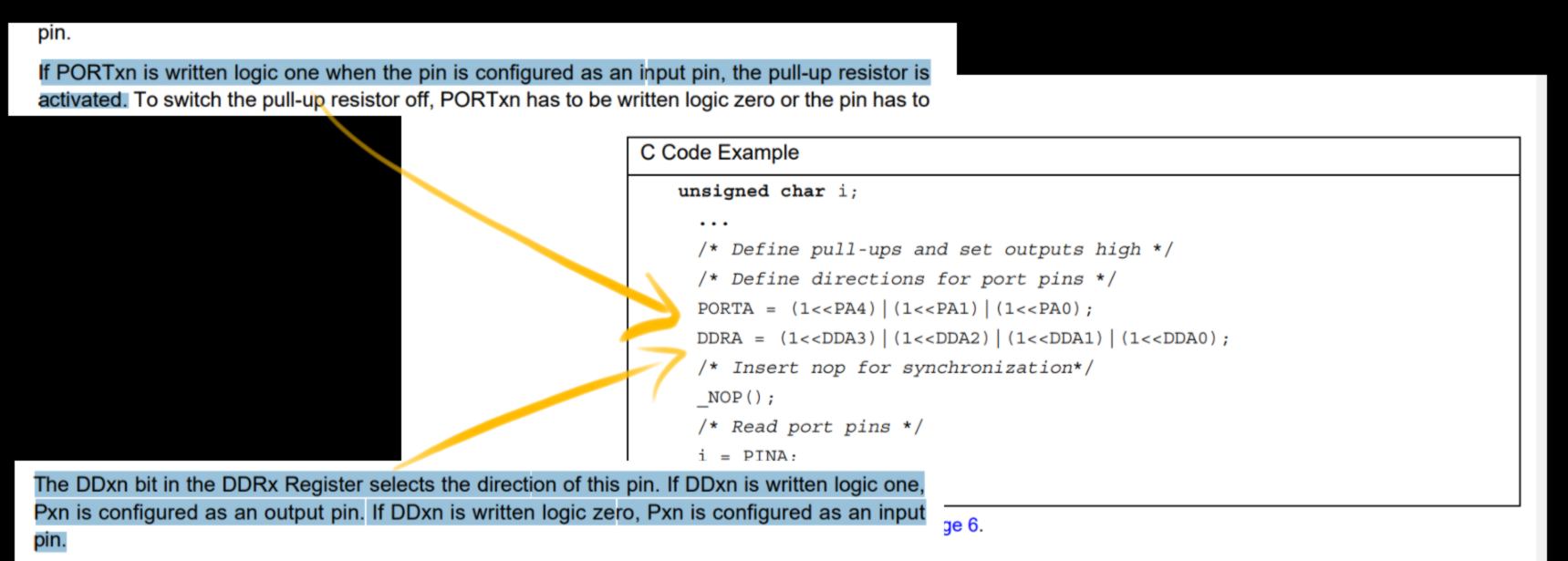
Each pin can be configured using three registers bits :DDxn, PORTxn, and PINxn, accessed using specific addresses :
By configured I mean : as an input or output.
The following code example shows how to:
The alternate functions of each pin are then described :
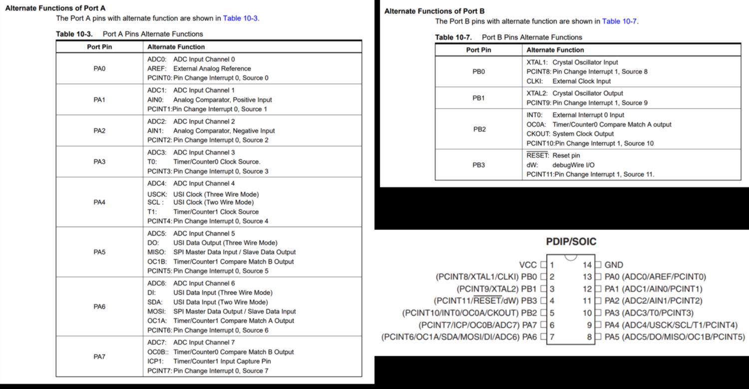
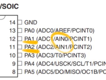
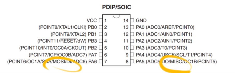
Pins on the port A are all Analog to Digital Converter; All pins are Pin Change Interrupt source. I will ask for human explanation later on this week.
I briefly skim through 8-bit and 16-bits Timer/Counter with PWM, allowing more or less accurate program execution timing, wave generation, and signal timing measurement. I notice that PA3 to 7 and PB2 can interact with this Timer/Counter system.
Out of curiosity I look for the way letters are written in binary. After all that is what switches are able to perform, and apparently the 8-bits systems was chosen ( rather than 5 of 9, true story?) since all letters of the latin alphabets and common punctuation signs fitted in:
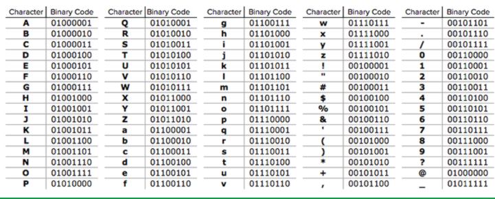
I add below an extract from a webpage that I find interesting :
"In the Pulitzer Prize-Winning book The Soul of a New Machine"(published in 1981)", author Tracy Kidder explains how Data General computers stored information in a binary language:
“Computers, it is often said, manipulate symbols. They don’t deal with numbers directly, but with symbols that can represent not only numbers but also words and pictures. Inside the circuits of the digital computer these symbols exist in electrical form, and there are just two basic symbols – a high voltage and a low voltage. Clearly, this is a marvelous kind of symbolism for a machine; the circuits don’t have to distinguish between nine different shades of gray but only between black and white, or in electrical terms, between high and low voltages.” Copyright © 1981 by John Tracy Kidder. Reprinted by permission of Little, Brown and Company, New York, NY. All rights reserved.
As computer technology has advanced, computer engineers have needed ways of sending and storing greater amounts of information at a time. As a result, the bit-length used by computers has been growing steadily over the course of computer history. If you have a new iPhone, it is using a 64-bit microprocessor, which means that it stores and accesses information in groups of 64 binary digits—which means that it’s capable of storing 264, or more than 18,000,000,000,000,000,000 unique 64-bit combinations of binary integers. Whoa."
I also go through the timer/Counter Prescaler description. this module is a circuit used to reduce a high frequency electrical signal to a lower frequency by division. Its purpose is to allow the timer to be clocked at a rate desired by a developper.
I move on to a description of the Universal Serial Interface (USI), providing hardware resources needed for communication : "the USI allows significantly higher transfer rates and uses less code space than solutions based on software only."
Then comes the analog comparator, compares the input values on the positive pin AIN0 and negative pin AIN1:
The user can trigger output rise, fall or toggle using this comparator. It is possible to configure any of the ADC[7:0] pins to replace the negative input to the Analog Comparator.
now we enter a quite long section about A to D conversion.
09.04.18 /I carry on my reading :
--- Analog to digital converter ---
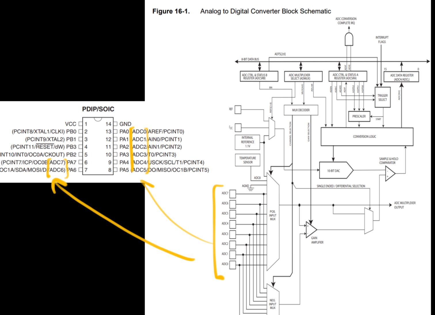
ATtiny24A/44A/84A features a 10-bit, successive approximation Analog-to-Digital Converter (ADC). Looking at what is a 10-bit ADC Converter, I end up on Sparkfun website mentioning in simple terms that :
"An Analog to Digital Converter (ADC) is a very useful feature that converts an analog voltage on a pin to a digital number. By converting from the analog world to the digital world, we can begin to use electronics to interface to the analog world around us."
"The ADC reports a ratiometric value. This means that the ADC assumes 5V is 1023 and anything less than 5V will be a ratio between 5V and 1023."
As a side-note :
"The way an ADC works is fairly complex. There are a few different ways to achieve this feat (see Wikipedia for a list), but one of the most common technique uses the analog voltage to charge up an internal capacitor and then measure the time it takes to discharge across an internal resistor. The microcontroller monitors the number of clock cycles that pass before the capacitor is discharged. This number of cycles is the number that is returned once the ADC is complete."
It seems that the system creates several small batches that are held then converted in digital numbers in 13 clock cycles. The internal reference voltage can be replaced by the Vcc. There is also an integrated temperature measurement system.
I go through the Debug system, emulating All On-chip Functions(except RESET Pin), and even find a summary of debugging command lines. The complexity of this chip is bottomless.
I discover that the device can selfprogram itself using "a Self-Programming mechanism for downloading and uploading program code by the MCU itself. The Self-Programming can use any available data interface and associated protocol to read code and write (program) that code into the Program memory."
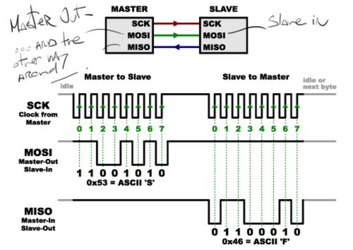
I then go through Memory Programming, and find an interesting bit about serial programming : "Both the Flash and EEPROM memory arrays can be programmed using the serial SPI bus while RESET is pulled to GND. The serial interface consists of pins SCK, MOSI (input) and MISO (output)."
This is, if I understand correctly, what our ISP uses. The pins used are not solely for Master to slave conmmunication, meaning that once the Flash memory is uploaded, these pins can be used for other purposes.
Then, the electrical characteristics of many modules are described. The ATtiny cannot take more than 6V Vcc, 40mA on I/O pins and 200mA on Vcc and Gnd pins. I quickly refresh my memory about current, voltage and resistance. A lot depends on voltage (and temperature) provided to the ATtiny. For example the clock speed varies.
The next section is the longest and by far the most visual one of the entire datasheet :
--- Typical Characteristics ---
On the next 82 pages I will find these charts :
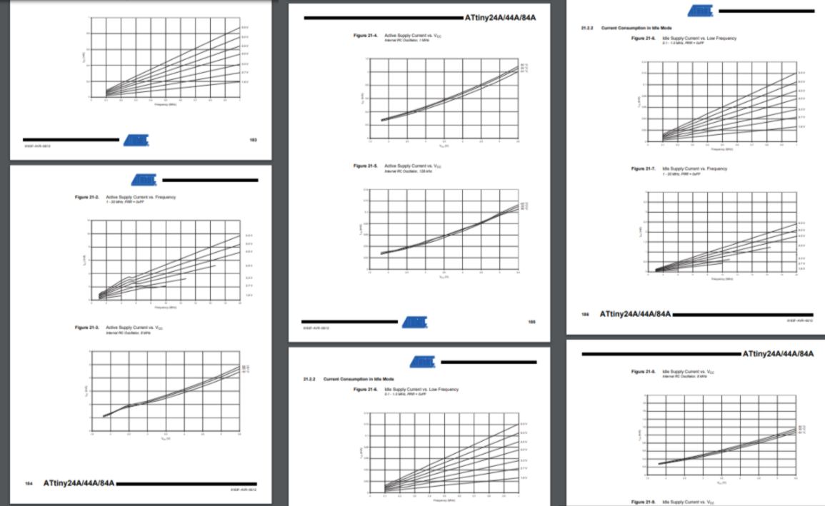
These charts shows the Current Consumption in different mode (Active, Power-Down, Reset) with different presets, oscillators, running at different frequencies. It also provides Current Consumption of Peripheral Units (including ADC)
As a side-note, I discover a new and elegant word : Hysteresis. It catches my interest but the scientific explanation makes no sense to me. The same term is used in other fields and described as : " Hysteresis is the lag between cause and effect.". Unelegantly visualised below :

The scientific definition : " the phenomenon in which the value of a physical property lags behind changes in the effect causing it, as for instance when magnetic induction lags behind the magnetizing force. " makes a lot more sense now.
This section is long since all three ATtiny (24A/44A/84A) consumption mode are described.
Then comes a Register Summary and Instruction Set Summary.
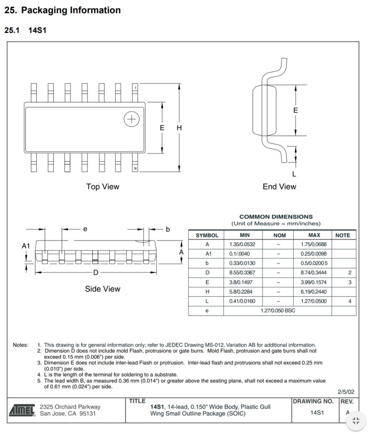
Finally, right before the table of Content ending the document, I find an Ordering information and Packaging information. The packaging information visually describes all different packaging for the same device (the only difference between the three models presented here is, as described above, memory space available)