Week 8 — Electronics Production
Assignments
Group Assignment
- Characterize the design rules for your in-house PCB production process: document feeds, speeds, plunge rate, depth of cut (traces and outline) and tooling.
- Document the workflow for sending a PCB to a boardhouse.
- Document your work on the group page and reflect on your learning on your individual page.
Individual Assignment
- Design, make, and test a microcontroller development board.
Learning Outcomes
- Describe the process of toolpath generation, milling, stuffing, debugging, and programming.
- Demonstrate correct workflows and identify areas for improvement if needed.
Introduction
This week was one of the most hands-on and challenging weeks of Fab Academy so far. The goal was to go through the complete process of making a printed circuit board (PCB) from scratch — starting from a digital design file in KiCad and ending with a physical, soldered board that you can actually program and test.
I had never made a real PCB before this week. I understood the basic concept but actually going through the whole process — designing the layout, exporting Gerber files, converting them to PNG, generating toolpaths in Mods CE, setting up the SRM-20 milling machine, choosing the right tools, milling the board, soldering all the components — was completely new to me. There are many individual steps and each one needs to be done correctly, because if you make a mistake early in the process you usually only find out much later after spending a lot of time and material.
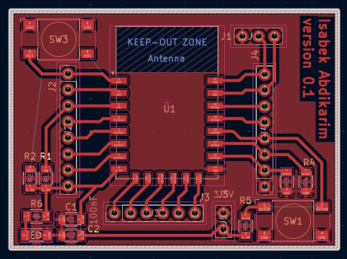
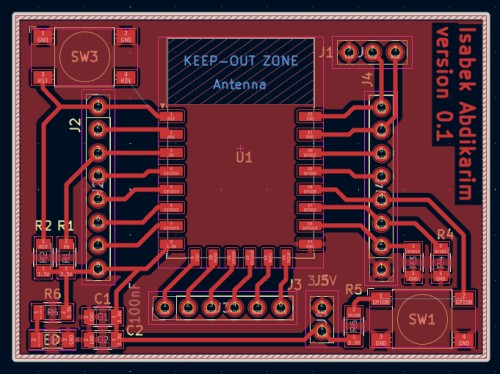
The board I designed is a microcontroller development board based on the ESP-32 chip. The ESP-32 is one of the most popular microcontrollers for embedded and IoT projects because it has built-in WiFi and Bluetooth, a dual-core 240 MHz processor, 34 GPIO pins, and it is cheap and very well supported with libraries and documentation. I designed my board around this chip with supporting components — resistors, capacitors, buttons, LED, and headers for connecting external modules and sensors. The board is labeled "Isabek Abdikarim version 0.1" which is the name I put in the KiCad silkscreen layer.
PCB Production Workflow Overview
Before going into the step-by-step details, here is the complete workflow from design to finished board. Every step depends on the previous one being done correctly:
| Step | Tool | Output |
|---|---|---|
| Design schematic and PCB layout | KiCad | .kicad_pcb file |
| Export Gerber files | KiCad Fabrication Outputs | .gbr layer files |
| Generate drill files | KiCad Generate Drill Files | .drl file |
| Convert Gerbers to PNG images | Gerber2PNG | .png image files |
| Generate NC milling toolpaths | Mods CE | .nc files |
| Set up and mill the PCB | Roland SRM-20 + VPanel | Physical milled board |
| Solder all components | Soldering iron + hot plate | Assembled board |
| Test and debug | Multimeter + computer | Working programmed board |
PCB Production Process
Step 1 — Export Gerber Files from KiCad
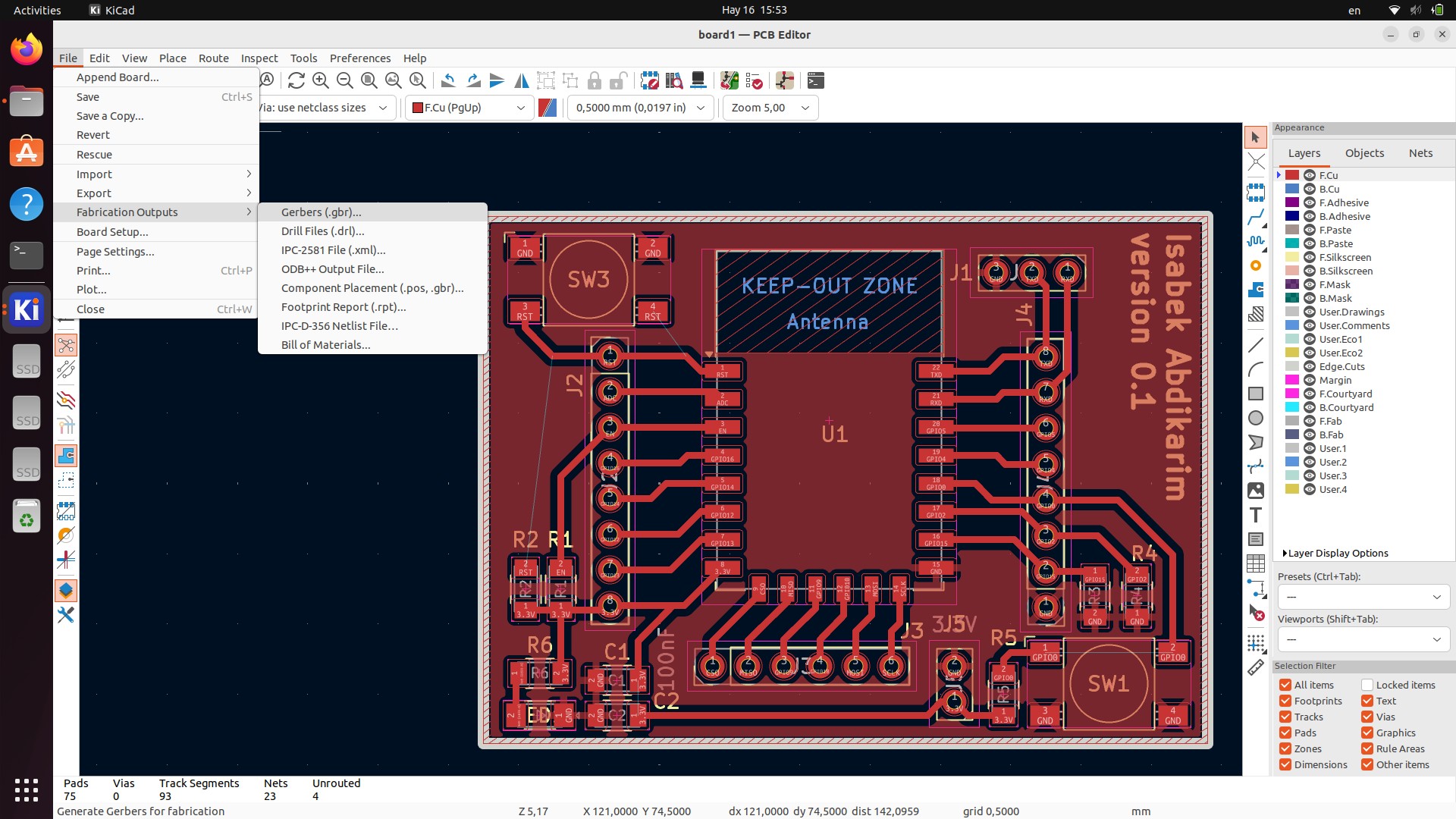
This screenshot shows the KiCad PCB Editor with the full board layout visible in the background while the File menu is open. The board design itself is clearly visible — the ESP-32 chip footprint labeled U1 sits in the center of the board, the two GPIO header rows (J1, J2, J4) run along the left and right sides, reset button SW3 is in the top left, boot button SW1 is in the bottom right corner, and the resistors, capacitors, and power connector are distributed around the board. In the top right area there is the large KEEP-OUT ZONE / Antenna region where no components or traces can be placed because the ESP-32's onboard antenna radiates from that area.
To start the file export I went to File → Fabrication Outputs which is visible in the open menu. From the submenu I selected Gerbers (.gbr) which is the first option. Gerber is the international standard file format for PCB manufacturing — every PCB manufacturer in the world accepts Gerber files, and all CAM tools including Mods CE use them as the starting point.
Looking at the status bar at the very bottom of the screen you can read: 75 Pads, 0 Vias, 93 Track Segments, 23 Nets, 4 Unrouted. The 4 unrouted connections were something I should have fixed before exporting — these are electrical connections that exist in the schematic but have no physical copper trace drawn on the PCB yet. This turned out to be directly related to the design errors I discovered later.
Step 2 — Configure Gerber Layer Settings
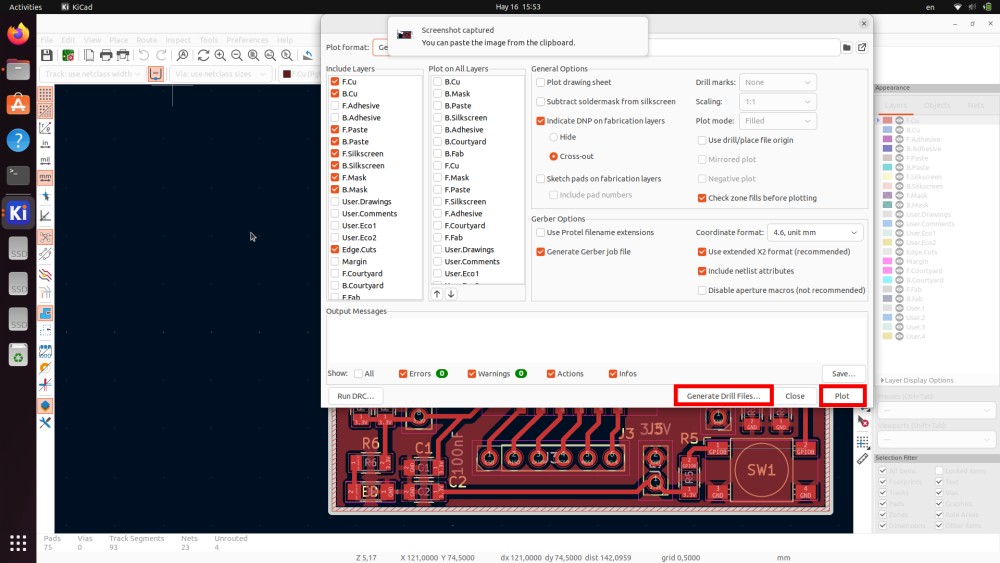
After clicking Gerbers in the menu, the Plot dialog opens. This dialog is where you configure exactly which layers to export and how the files should be formatted. In this screenshot you can see the complete dialog with the layer list on the left, the "Plot on All Layers" column in the middle, and the General Options and Gerber Options panels on the right.
The layers I enabled for export in the left column:
- F.Cu — the front copper layer containing all traces and pads. This is the single most important layer because it defines the entire electrical circuit on the board.
- B.Paste and F.Paste — paste layers for solder paste application
- F.Silkscreen and B.Silkscreen — the white printed labels showing component reference designators and board name
- F.Mask and B.Mask — the solder mask layers that define where copper is exposed
- Edge.Cuts — this is the board outline layer and it is absolutely required for the cutout milling operation
On the right side under Gerber Options I set the Coordinate format to 4.6, unit mm which is the standard precision format that Gerber2PNG and other tools expect. I also kept "Generate Gerber job file" and "Use extended X2 format (recommended)" checked — these produce additional metadata that helps verify the export integrity.
The important thing visible at the bottom of the dialog is the "Generate Drill Files..." button. After clicking Plot to export the Gerbers I immediately clicked this button to generate the drill file, keeping everything in the same export session so the coordinate origins would definitely match.
Step 3 — Generate Drill Files
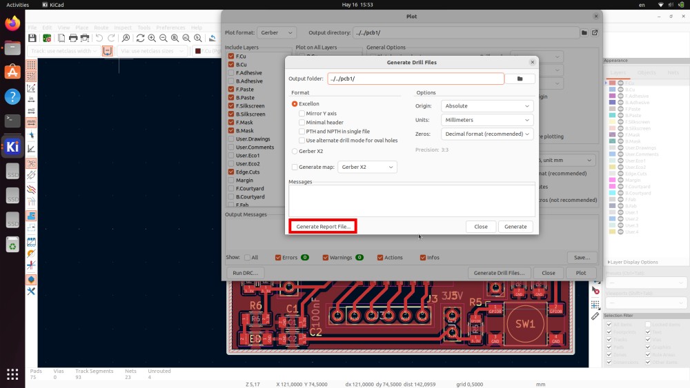
This screenshot shows the Generate Drill Files dialog which opens after clicking the "Generate Drill Files" button from the Plot dialog. The drill file is a separate file from the Gerber layers and it is just as critical — it tells the milling machine exactly where to place drilling operations for through-hole component pins, mounting holes, and any via holes.
The settings visible in this dialog:
- Output folder: set to the same folder as the Gerber files so everything stays organized together
- Format: Excellon — this is the universal standard drill file format accepted by the SRM-20 and all other milling machines. The option "Use alternate HMI mode for ViewMates" was left unchecked as it is only needed for specific verification software.
- Units: Millimeters — consistent with the millimeter units used throughout the PCB design in KiCad
- Zeros: Decimal format (recommended) — the modern way to specify coordinates that avoids any ambiguity about where the decimal point is
- Origin: Absolute — this means drill positions are given as absolute coordinates from the design origin
The "Generate Drill Report Files" button highlighted with the red box is what actually creates the file. After clicking it KiCad generates the .drl file and shows a confirmation in the Messages area.
One critical thing: the drill file and the Gerber files must use exactly the same coordinate origin. If they use different origins, the drill holes will be offset from the pads and the board will be unusable — you would have holes that do not align with any component. Setting both to Absolute origin ensures they are always consistent.
Converting Gerber Files to PNG
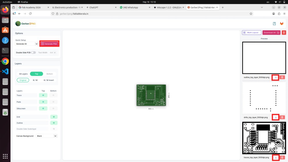
The Roland SRM-20 does not read Gerber files directly. The CAM tool we use — Mods CE — takes PNG images as input rather than Gerber files. So the next step was to convert each Gerber layer into a black and white PNG image using Gerber2PNG, a free online tool available at gerber2png.fablabkerala.in. This tool was developed by the Fab Lab Kerala team specifically for this workflow.
In this screenshot you can see the Gerber2PNG interface open in Firefox. The tabs at the top of the browser window show that I had multiple pages open — Fab Academy, the electronics production assignment, ChatGPT, WhatsApp, Inkscape, and Gerber2PNG — which shows how many different things needed to be running at the same time during this process.
On the left side of the Gerber2PNG interface there are the configuration options — Canvas Background set to Black, layers panel showing Trace, Pads, Silkscreen, Drill, and Outline rows each with Top and Bottom toggle options. In the center of the page there is a color preview of the PCB showing the green board with all the component footprints visible — this is a useful visual check to confirm the Gerber files loaded correctly before generating the PNG outputs.
On the right side you can see the three generated PNG files with download buttons:
- outline_top_layer_3000dpi.png — a simple outline of the board shape, white boundary on black background. Used for the final cutout operation that separates the board from the material.
- drills_top_layer_3000dpi.png — shows each drill position as a small white dot on black. Used to generate the drilling toolpath.
- traces_top_layer_3000dpi.png — the most detailed and important file, shown at the bottom right. It is a high resolution black and white image of all the copper traces where white areas represent copper to keep and black areas represent copper to remove.
The resolution of 3000 DPI is important here. Higher resolution means more pixels per millimeter, which means the milling machine can distinguish finer trace details. I initially tried 1000 DPI but the small pads looked blurry at the edges, so I increased to 3000 DPI for cleaner results.
Preparing NC Files in Mods CE
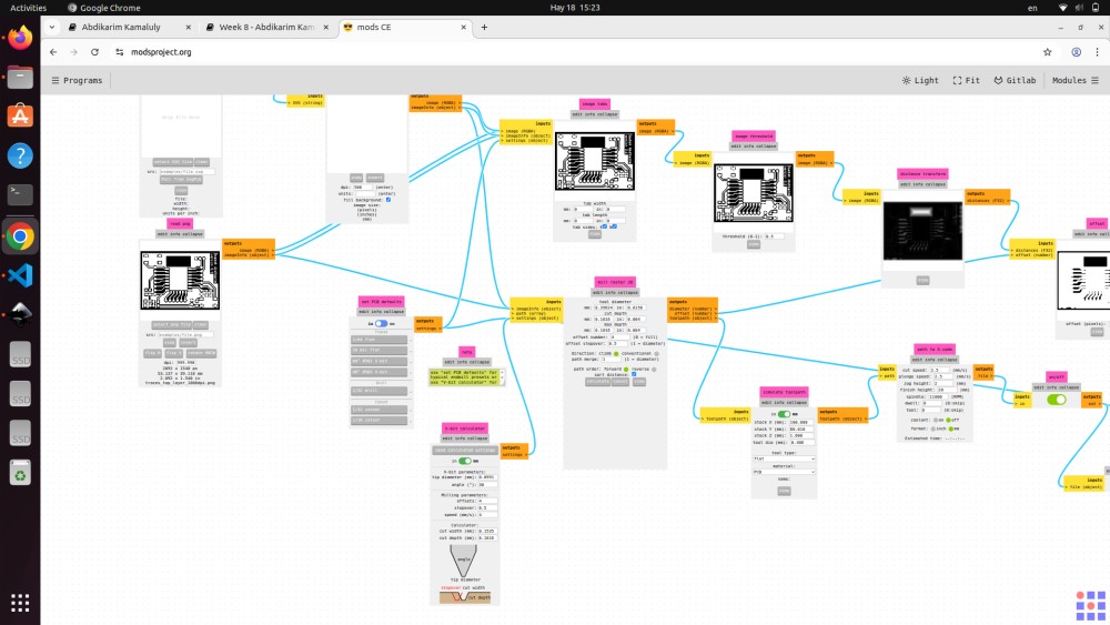
Mods CE is an open source browser-based CAM tool developed at MIT and used in Fab Labs worldwide. It converts the PNG images from Gerber2PNG into NC (numerical control) files that the Roland SRM-20 can execute. This screenshot shows the complete Mods CE interface with the Mill 2D PCB workflow loaded.
The interface is a visual node programming environment — each colored block is a processing module and the cyan lines show how data flows between them from left to right. It looks overwhelming at first but the logic is straightforward once you understand the structure:
- Left side of the graph — input nodes where the PNG images are loaded. You can see small black and white thumbnail previews of the trace and outline images in the leftmost blocks.
- Center of the graph — processing nodes that analyze the image, calculate the toolpath offset, and generate the cutting coordinates. The orange/yellow nodes are parameter inputs (tool diameter, cut depth, feed rate), the pink nodes are operations, and the grey nodes display status information.
- Right side of the graph — output nodes showing the final toolpath preview as a white-on-black image and the NC file export button.
Looking at the parameter nodes visible in the graph I can read some of the settings I used for the trace milling toolpath — tool diameter, offset passes, cut depth, speed values. I processed three completely separate NC files one at a time:
| NC File | Purpose | Tool | Cut Depth | Feed Rate |
|---|---|---|---|---|
| Traces NC | Isolate copper traces | 0.4mm V-bit | 0.1 mm | 4 mm/s |
| Drill NC | Drill component holes | 0.8mm end mill | Through board | 2 mm/s |
| Outline NC | Cut board perimeter | 0.8mm end mill | Through board | 2 mm/s |
Each file required loading the corresponding PNG, setting the appropriate tool parameters, running the path generation, and downloading the resulting NC file. After generating all three files I had everything needed to start the milling process.
SRM-20 Milling Machine
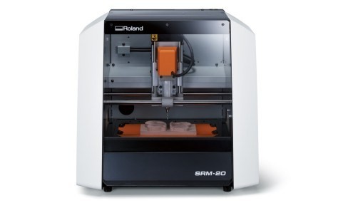
This is the Roland SRM-20 — the desktop CNC milling machine we used for physically producing the PCB. The machine is clearly visible in this photo: the white and black body, the orange spindle head mounted on the gantry that moves in X, Y, and Z directions, and the flat rectangular machine bed where the PCB material is fixed.
The SRM-20 is standard equipment in Fab Labs around the world and is specifically designed for small precision work — PCB milling, wax mold carving, small engraving jobs. Understanding how it works mechanically helps make sense of the whole process.
The machine works by spinning a very small cutting tool at high RPM and moving it across the surface of the material in precise X, Y, and Z coordinates as defined by the NC file. For PCB milling specifically, it cuts away the thin copper layer from the top of the copper-clad board, leaving only the copper traces and pads that form the circuit. The areas where copper is removed become the isolation channels between traces.
Key specifications of the SRM-20:
| Specification | Value |
|---|---|
| Work area | 203 × 152 × 60 mm |
| Positioning accuracy | 0.01 mm |
| Maximum spindle speed | 7,000 RPM |
| Minimum trace isolation | ~0.1 mm with right tool |
| Interface | USB to VPanel software |
| Control software | Roland VPanel |
The main challenge with PCB milling on the SRM-20 is achieving a consistent cut depth across the entire board surface. If the board is not perfectly level — even a 0.1 mm tilt — the cut will be too shallow on one side and too deep on the other, producing inconsistent trace quality. This is why leveling and careful Z-axis zeroing before milling is so important.
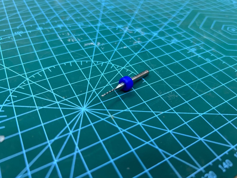
Cutting Tools
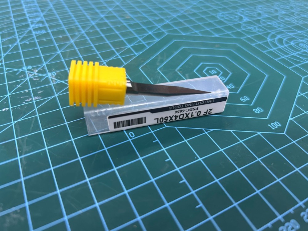
These two photos show the cutting tool used for milling the copper traces on the PCB. The first photo shows the complete tool next to its protective packaging — you can see the yellow plastic cap that protects the delicate tip when the tool is stored. The label on the packaging clearly shows the tool specification: 2F 0.1XD4X60L by PSDC, which describes a 2-flute V-bit with a 0.1mm tip, 4mm shank diameter, and 60mm total length.
The second photo gives a closer view of the tool itself, showing the sharp pointed V-shape of the cutting tip. This V geometry is the key feature of the tool — when it cuts into the copper surface, the width of the cut depends directly on the depth of cut. At 0.1mm depth the cut is very narrow and precise, which is what you need to isolate thin traces from each other. At greater depths the V-shape would produce wider cuts, which is useful for clearing large copper areas but risks cutting into adjacent traces if used carelessly.
For my board I used two different tools in sequence:
V-bit 0.1mm tip — for milling traces: This tool is used exclusively for the trace isolation pass. It is extremely fragile because of the very fine tip — if the Z zero is set even slightly too deep, or if the board lifts during milling, or the feed rate is too high, the tip will snap. Each tool costs a few euros and keeping spares is essential. After mounting this tool in the spindle collet I re-zeroed the Z axis carefully using the paper method — sliding a thin paper between the tool tip and the board surface until it just barely grips, indicating contact.
Flat end mill 0.8mm — for drilling and outline: After the trace milling is complete, the tool must be changed to the larger 0.8mm flat end mill for the drilling and outline operations. This tool is much more robust and can cut through the full 1.6mm board thickness. Changing tools requires re-zeroing the Z axis again because every tool has a slightly different length in the collet.
Milling in VPanel
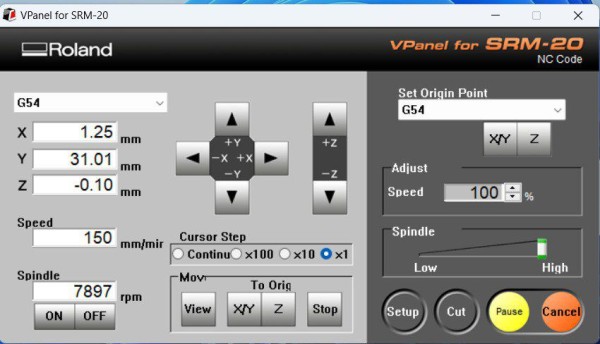
This screenshot shows VPanel for SRM-20 — the Roland control software on the connected computer — during an active milling session. The interface is in NC Code mode which is used for loading and running the NC files generated in Mods CE.
Reading through all the information shown in the interface:
On the left side, the position display shows the real-time coordinates of the spindle: X = 1.25 mm, Y = 31.01 mm, Z = -0.10 mm. The Z value of -0.10 mm is significant — it means the tool tip is currently 0.1mm below the zero surface, which is exactly the cut depth programmed for the trace isolation pass. This confirms the milling is running at the correct depth.
The Speed field shows 150 mm/min — this is the horizontal feed rate at which the tool moves through the copper. For the trace isolation pass this speed needs to be conservative to avoid breaking the fragile V-bit tip.
The Spindle section shows 7897 RPM with the ON button active — the spindle is running at nearly 8000 RPM. At this speed the cutting tool makes clean cuts through the thin copper layer without tearing or pulling the copper up.
On the right side, the Set Origin Point section with G54 coordinate system and the separate X/Y and Z buttons is how I set the origin before starting. I jogged the tool to the bottom-left corner of where my board would be, pressed X/Y to set that as the horizontal zero, then carefully lowered the tool to the board surface and pressed Z to set the vertical zero.
The Adjust Speed slider at 100% means the machine runs at exactly the speed defined in the NC file. The Cursor Step set to ×1 was used for the fine jogging movements when positioning the tool precisely before starting.
The milling sequence I followed was strictly: traces first → drill holes second → outline last. This order is not optional — cutting the outline last is essential because it is the cut that separates the board from the surrounding material. If you cut the outline first, the board becomes loose and all subsequent milling passes will shift and destroy the work. Doing the drill holes before the outline ensures the board is still firmly attached when the vibration of drilling happens.
Preparing Components for Soldering
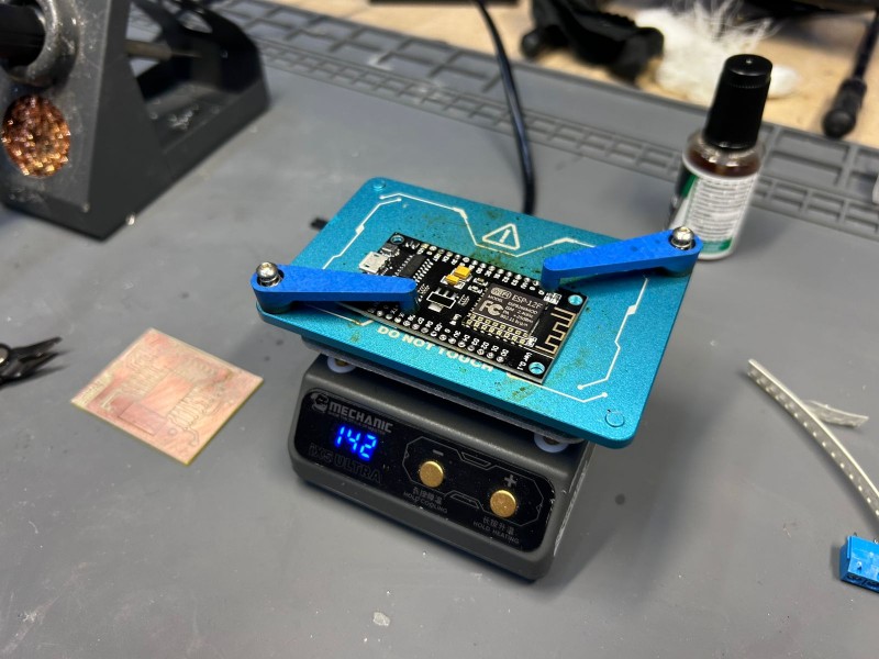
This photo shows the soldering station set up for assembling the board. Several things are visible that are worth explaining in detail.
The blue anodized aluminum fixture holding the board is a PCB soldering holder — a frame with four adjustable corner clamps that grip the board edges and hold it completely flat and stable. This is very useful for SMD work because you need both hands free — one for the iron and one for tweezers holding the tiny component. Without a fixture the board slides around and you end up burning your fingers trying to hold everything at once.
The Mechanic hot plate underneath is a preheating tool showing 142°C on the blue digital display. A hot plate heats the PCB from below before and during hand soldering, which gives several advantages. The solder melts more easily and flows better onto the pads when the board is already warm. You spend less time holding the iron on each component pad, which reduces the risk of heat damage to sensitive components or pad delamination. For SMD soldering of very small components like 0402 resistors, preheating the board to 120–150°C before touching it with the iron makes a significant difference in joint quality.
In the background you can see a flux bottle — liquid flux that I applied to pads before soldering. Flux is a chemical that removes oxidation from metal surfaces and helps solder flow and bond cleanly. Using flux especially on the small ESP-32 pads helps prevent cold joints and solder bridges between adjacent pads.
The milled PCB is visible inside the blue fixture — you can see the copper surface with the milled trace channels. The traces are clearly defined and the isolation channels between them look clean and even, indicating the milling was done at the correct depth and speed.
The component list for this board was:
| Component | Specification | Quantity |
|---|---|---|
| ESP-32 chip | Main microcontroller, WiFi + Bluetooth | 1 |
| Resistors | 1002 Ohm (1 kOhm), 0402 SMD | 5 |
| Pin headers | 1x08 straight | 1 |
| Pin headers | 1x03 straight | 1 |
| Pin headers | 1x02 straight | 1 |
| LED | 3mm | 1 |
| Tactile buttons | 6mm through-hole | 2 |
Board Completion
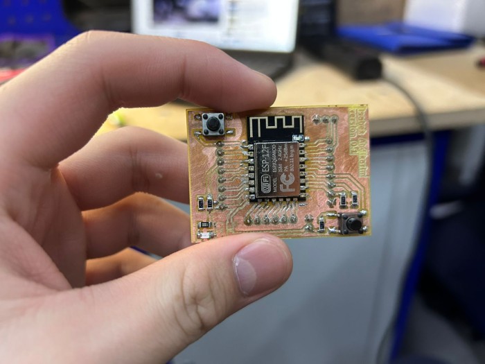
This photo shows the finished and fully assembled PCB held in a hand. This is the end result of all the work this week — the board started as a digital design in KiCad and is now a real physical electronic device with all components soldered in place.
Looking at the board carefully in this photo you can see:
The ESP-32 module is soldered in the center of the board. The metallic RF shield on top of the module is visible, and you can see the WiFi antenna structure at one edge of the module. The module is soldered using the castellated pads along its two long edges which connect to the corresponding pads on the milled board.
The small rectangular SMD resistors in 0402 package are visible as tiny components on the pads around the ESP-32. These are approximately 1.0 × 0.5 mm in size — small enough that they can be accidentally picked up by static electricity or moved by a breath of air. Soldering them required fine-tipped tweezers, flux, and steady hands.
Both tactile push buttons are visible — the reset button in the upper left area of the board and the boot button in the lower right. These are standard 6mm through-hole buttons. The boot button is essential for programming the ESP-32 — you hold it while pressing reset to put the chip into bootloader mode, which is required for flashing new firmware over USB.
The milled copper traces are clearly visible on the board surface as the thin copper lines connecting all the component pads. The trace isolation channels cut by the V-bit are the darker lines separating the traces. The quality of the milling looks consistent across the board.
The board size is approximately 50 × 35 mm, which you can judge from the hand holding it. This is a compact size that is suitable for integration into the robotic manipulator project as the main controller board.
After completing the soldering I did a visual inspection under magnification and checked the key power and programming connections with a multimeter in continuity mode before connecting any power.
Design Errors Found
These two screenshots show my PCB design in KiCad at different points during the design process. Comparing them closely reveals the errors I found after the board was already produced and assembled.
Both screenshots show the complete PCB layout: the ESP-32 footprint (U1) in the center, the GPIO headers (J1, J2, J4) on both sides, resistors R1 through R6 placed around the board, capacitors C1 and C2 in the lower left area, both buttons SW1 and SW3, and the KEEP-OUT ZONE for the antenna area. The board looks complete at first glance.
However, looking carefully at the second screenshot compared to the first, you can notice differences near the bottom left area around the capacitors. In the second screenshot the component label near that area shows F1 instead of R1, indicating that the component reference was changed or the connection was not properly completed. More importantly, looking at the status bar in the first screenshot it clearly shows 4 Unrouted connections — meaning four electrical connections from the schematic had no copper trace on the PCB.
Problem 1 — Capacitors C1 and C2 not properly connected to power net:
The two bypass capacitors visible in the bottom left area of the board were placed correctly in terms of physical position, but their connections to the power supply net were not completed in the routing. In KiCad, when a connection exists in the schematic but has no trace drawn, it shows as a thin ratsnest line on the board. I must have missed these ratsnest lines during my design review. Bypass capacitors on the power pins of the ESP-32 are critical for stable operation — they filter high-frequency noise on the power supply line, especially when the WiFi radio is active and drawing brief bursts of current. Without them the chip can have erratic behavior or fail to boot.
Problem 2 — Missing pull-up resistor connection on the RST line:
The reset line of the ESP-32 requires a pull-up resistor to keep the pin in the HIGH state during normal operation. Without this resistor the RST pin is floating — it has no defined voltage level and can be triggered by electrical noise, causing random resets or preventing the board from starting correctly. I had the resistor placed in the design but the trace connecting it to the 3.3V net was not routed.
Both of these problems were directly visible in the design — the 4 Unrouted count in the KiCad status bar was showing exactly these missing connections the entire time I was working on the design. Running the ERC (Electrical Rules Check) would have immediately flagged all unconnected pins as errors. The lesson is simple and important: never skip the ERC before exporting files, and take time to understand and fix every warning it reports.
Conclusion and Future Improvements
This week was one of the most educational and challenging weeks of Fab Academy. For the first time I went through the complete hardware production pipeline from a digital schematic to a physical board in my hands. Even though the first version had design errors, understanding exactly why they happened and what they affect was genuinely valuable learning.
What I learned this week:
- The complete KiCad workflow from PCB layout design through Gerber and drill file export
- How to use Gerber2PNG to convert design files into the raster images required by Mods CE
- How to configure Mods CE toolpaths with the correct tool parameters for traces, drilling, and outline
- How to operate the Roland SRM-20 safely — setting coordinate origins, loading NC files, monitoring cuts
- Why the milling sequence matters and must always be traces then drill then outline
- How to use a hot plate as a preheater to improve SMD soldering quality
- How to solder 0402 SMD components with tweezers, flux, and a fine-tip iron
- How to debug a board — visual inspection, multimeter continuity testing, reading design files
- How to interpret KiCad ERC and DRC warnings and why they should never be ignored
What I will do differently for version 0.2:
- Run the ERC and DRC before exporting any files and fix every single warning — no exceptions
- Do a test milling pass on scrap copper material before milling the actual board to verify tool settings and Z zero
- Complete all trace routing so there are zero unrouted connections before export
- Check the ratsnest lines carefully before finishing the PCB layout — every thin line is a missing connection
- Use the Gerber Viewer in KiCad to visually inspect every exported layer before moving forward
- Solder the ESP-32 last so I can work freely on all other components first
Next steps:
The plan is to fix the two design errors — connect the capacitors to the power net and complete the RST pull-up resistor routing — and produce version 0.2 of the board. The fixes are straightforward in KiCad and should take no more than an hour. Once the corrected board is milled and assembled I will program it and use it as the main controller for the robotic manipulator arm in the final project.
Fab Academy 2026 · YU FabLab · Abdikаrim