Week 6 — Electronics Design with KiCad
Group Assignment
Before starting the individual PCB design work, our group carried out this week's group assignment, which focused on hands-on use of essential electronics lab equipment: a digital multimeter, a two-channel oscilloscope, and a logic analyzer. The goal was to get comfortable measuring and interpreting both analog and digital electrical signals, since these instruments are exactly what we will rely on later when debugging our own boards.
Multimeter measurements. We started with a UNI-T digital multimeter — a compact, backlit handheld unit that is convenient to use even in low-light lab conditions. Using a WANPTEK bench DC power supply, an LED, an Arduino board as a test platform, and connecting wires, we built a simple LED test circuit. The power supply was set to approximately 2.4V, and the multimeter was connected in parallel with the load to measure voltage, reading back about 2.44V — confirming that the power supply output was stable and accurate. We then reconnected the multimeter in series with the circuit to measure current, recording roughly 0.14A on the power supply display while the multimeter confirmed the circuit was drawing current safely within expected limits. These readings were cross-checked against Ohm's Law (I = V/R), and the measured current matched the behavior expected from the applied voltage and the resistor value in the circuit. The LED operated correctly throughout, confirming that the circuit design and component selection were correct.
Oscilloscope measurements. Next, we moved on to a two-channel digital oscilloscope to examine a more dynamic, real-world signal: the PWM control signal driving a brushless DC motor (BLDC) through an Electronic Speed Controller (ESC), the kind of setup used in drone propulsion systems. One oscilloscope channel was connected to the motor control signal line, while the second channel was used optionally to compare against the power line. Unlike a multimeter, which only shows averaged voltage or current, the oscilloscope let us actually see the waveform shape in real time. We observed that the control signal was a Pulse Width Modulation (PWM) signal, and that both its frequency and duty cycle changed depending on throttle input — exactly what is expected from correct ESC operation. The waveform amplitude stayed stable throughout, and the overall shape confirmed the ESC was generating a clean, properly behaving control signal. This step highlighted why an oscilloscope is indispensable for high-speed systems: it lets you visualize waveform shape, measure frequency and duty cycle, and catch noise or instability that a multimeter simply cannot reveal.
Logic analyzer measurements. Finally, we used a logic analyzer to dig deeper into the purely digital side of the same motor control setup, connecting it to the control signal line between a microcontroller (Arduino / flight controller) and the ESC. While the oscilloscope shows continuous analog waveforms, the logic analyzer is built specifically to capture and decode digital timing — clean HIGH/LOW transitions, exact pulse widths, and communication protocol behavior. We captured the digital PWM pulses being sent to the ESC and watched the pulse width change smoothly as throttle input was adjusted, with no significant noise on the line and timing behavior that matched the expected PWM characteristics for motor control. This confirmed that the digital control signal driving the brushless motor was being generated and transmitted correctly.
Comparing the three tools. Working through all three instruments back-to-back made the differences between them very concrete: the multimeter measures voltage and current as steady-state values, the oscilloscope reveals waveform shape, frequency, and duty cycle for both analog and mixed signals, and the logic analyzer is purpose-built for capturing digital timing and protocol-level behavior. Combining all three gave us a much more complete picture of how a real embedded system — in this case a drone-style BLDC motor driven by an ESC — actually behaves electrically, from the basic DC voltage and current levels all the way down to the precise digital timing of the control pulses. This exercise reinforced debugging skills that will be directly useful for verifying the ESP8266 board designed later this week, and more broadly for any embedded systems or hardware prototyping work going forward.
The full write-up with photos, the equipment lists, and additional observations for this group assignment is available on the lab's site: group assignment page.
Hero shot
Introduction
This week was dedicated to electronics design — specifically designing a custom PCB (Printed Circuit Board) from scratch using KiCad 9.0. PCB design is one of the most critical skills in electronics engineering, and Fab Academy provides an excellent opportunity to learn the complete workflow: from drawing a schematic, selecting and placing components, routing copper traces, defining board boundaries, all the way to producing files ready for fabrication or CNC milling in the lab.
The board I designed this week is an ESP8266-based development board using the popular ESP-12E module. The ESP8266 is a low-cost Wi-Fi enabled microcontroller that has become a staple in IoT (Internet of Things) projects worldwide. My goal was to design a clean, functional breakout board that exposes all the GPIO pins of the ESP-12E, includes proper power filtering, a reset circuit, and a UART interface for programming — essentially a custom alternative to commercial ESP8266 dev boards.
Why KiCad?
Before diving into the design process, it is worth explaining why KiCad was chosen over other available EDA (Electronic Design Automation) tools. The EDA software landscape includes many options, each with their own strengths and limitations.
Eagle by Autodesk was for many years the industry standard for hobbyists and small companies. However, since Autodesk acquired it, the free version has become severely limited — restricted to 2 schematic sheets and a maximum board area of 80 cm². For anything beyond simple projects, a paid subscription is required. Additionally, Eagle's scripting capabilities are limited compared to KiCad.
EasyEDA is a browser-based tool that has gained popularity due to its tight integration with LCSC components and JLCPCB manufacturing. However, being entirely cloud-based means you cannot work offline, your design files are stored on their servers, and the tool's capabilities for complex designs are more limited. It is excellent for quick, simple boards but not ideal for a serious design workflow.
Altium Designer is arguably the most powerful PCB design tool in the world, used by professional engineering teams at major companies. However, a full license costs approximately $7,000 per year — completely out of reach for students and hobbyists. Altium does offer a student version, but with significant limitations.
KiCad, on the other hand, is completely free and open-source, developed by a large community and supported by CERN (the European Organization for Nuclear Research). It has absolutely no limitations on board size, number of schematic sheets, or any other design parameters. It runs entirely offline on your local machine, meaning your design files are always in your hands. The scripting interface using Python is powerful and well-documented. Most importantly for Fab Academy students, the official PCM_fab component library is built specifically for KiCad, containing all the components available at Fab Labs worldwide with correct footprints verified by the Fab Academy community.
| Feature | KiCad 9 | Eagle (free) | EasyEDA | Altium Designer |
|---|---|---|---|---|
| Price | Free & open-source | Free (limited) | Free (cloud) | ~$7,000/year |
| Board size limit | Unlimited | 80 cm² | Unlimited | Unlimited |
| Schematic sheets | Unlimited | 2 sheets | Unlimited | Unlimited |
| Offline use | ✅ Full | ✅ Full | ❌ Cloud only | ✅ Full |
| Python scripting | ✅ Built-in | ❌ No | ❌ No | ✅ Built-in |
| 3D viewer | ✅ Built-in | ✅ | ❌ Limited | ✅ |
| Fab Academy library | ✅ PCM_fab | ❌ | ❌ | ❌ |
| Community & docs | ✅ Excellent | ✅ Good | ✅ Good | ✅ Excellent |
| Gerber export | ✅ | ✅ | ✅ | ✅ |
| Active development | ✅ Very active | ⚠️ Slow | ✅ Active | ✅ Active |
The conclusion is clear — for Fab Academy and for open-source hardware design in general, KiCad is the best tool available. It is what professionals, researchers at CERN, and the Fab Academy community all use.
Setting Up KiCad

KiCad 9.0 was installed on Ubuntu Linux. After creating a new project (board1.kicad_pro), the main KiCad project manager window opens, showing the project file tree on the left and the available tools on the right.
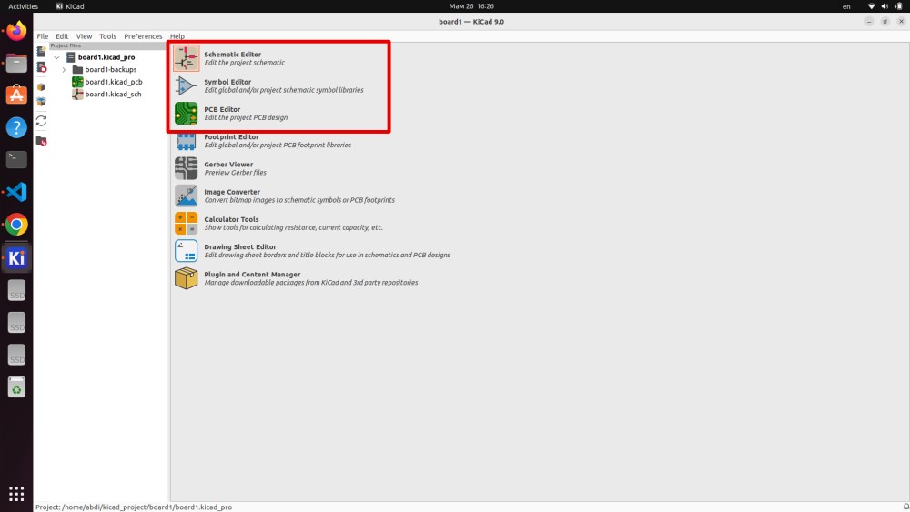
The three most important editors highlighted in the main window are:
Schematic Editor
The Schematic Editor is where the entire logical design of the circuit lives. Here you place component symbols, draw wires to connect them, add power symbols, net labels, and hierarchical sheet references. The schematic has no concept of physical dimensions — a resistor symbol is just a rectangle with two pins, regardless of whether the actual component is a 0402 or a 1206 package. The schematic defines the electrical intent of the design: which pins are connected to which nets, what components are used, and what the overall circuit topology is.
Working in the schematic editor, you build up a complete picture of your circuit. Every connection you make here becomes a "net" — a named group of electrically connected pins. When you later move to the PCB editor, these nets are represented as "ratsnest" lines (thin white lines showing which pads need to be connected by copper traces). The schematic is the single source of truth for your design, and any changes to connectivity must always be made here first, then synchronized to the PCB.
Symbol Editor
The Symbol Editor is a dedicated tool for creating and modifying schematic symbols. A symbol is the graphical representation of a component in the schematic — for example, an op-amp is drawn as a triangle with input and output pins, a capacitor is two parallel lines, a microcontroller is a rectangle with many labeled pins on all four sides.
KiCad ships with thousands of symbols covering virtually every common component category. However, for specialized or new components, you may need to create a custom symbol. The Symbol Editor lets you draw pin lines, add labels, set pin numbers, define pin types (input, output, bidirectional, power, passive), and organize symbols into libraries. Custom symbols created here can be saved to a project-specific library so they are portable with your design.
PCB Editor
The PCB Editor is where the physical board design happens. Once the schematic is complete, you synchronize it with the PCB editor, which imports all component footprints and the ratsnest connectivity. A footprint is the physical representation of a component — the exact pad dimensions, spacing, courtyard, silkscreen outline, and 3D model that correspond to the real-world package of the component.
In the PCB editor you work with layers: copper layers (F.Cu for front, B.Cu for back), silkscreen layers (F.Silkscreen, B.Silkscreen), mask layers (F.Mask, B.Mask), courtyard layers, fabrication layers, and the Edge.Cuts layer for the board outline. You place footprints, move them around to find the optimal arrangement, then route copper traces between pads following the ratsnest connections. You can also add text, logos, copper zones (filled areas), vias (connections between layers), and design rule violations are caught in real time.
Adding the Fab Academy Component Library
One of the first and most important steps before starting any design for Fab Academy is to add the official PCM_fab component library. This library was created and is maintained by the Fab Academy community and contains components that are:
- Verified to be available at Fab Labs globally
- Equipped with accurate, tested footprints matching the actual physical packages
- Organized with clear naming conventions and descriptions
- Accompanied by datasheets and reference information
Without this library, you would need to search through KiCad's generic libraries and hope that footprints match your available components — a risky approach that can lead to assembly problems.
Step 1 — Install via Plugin and Content Manager
The PCM_fab library is most easily installed through KiCad's built-in Plugin and Content Manager (PCM). Open it from the main KiCad window, search for "fab", and install the Fab Electronics Library package. This automatically downloads the library and places it in the correct directory (${KICAD9_3RD_PARTY}).
Step 2 — Open the Library Manager
Navigate to Preferences → Manage Symbol Libraries from the main KiCad window.
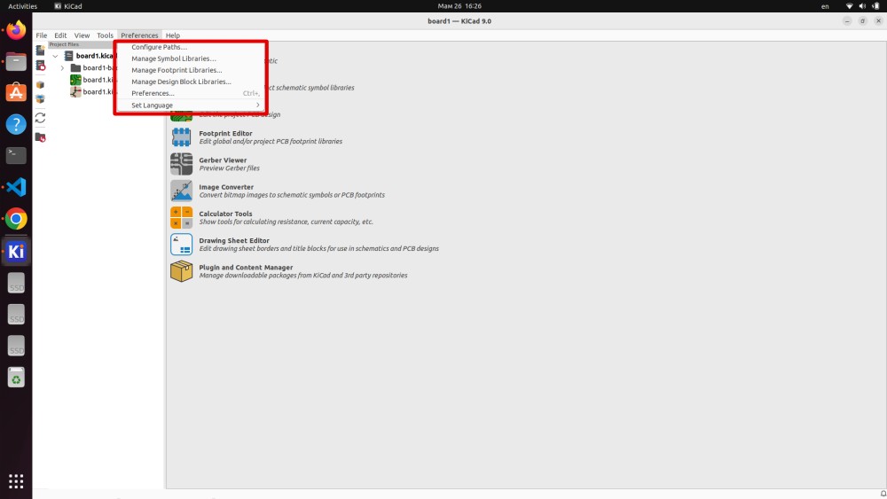
The Preferences menu also shows other important options: Configure Paths (where KiCad looks for libraries and other resources), Manage Footprint Libraries (for PCB footprints, separate from schematic symbols), Manage Design Block Libraries, and the general Preferences dialog for KiCad's behavior and appearance settings.
Step 3 — Confirm the Library is Added
After installation, verify that the PCM_fab library appears in the Global Libraries tab of the Symbol Libraries dialog.
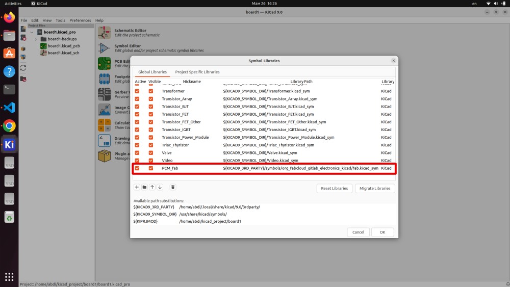
The library path shown is:
${KICAD9_3RD_PARTY}/symbols/org_fabcloud_gitlab_electronics_kicad/fab.kicad_sym
The path variables resolve as follows:
- ${KICAD9_3RD_PARTY} → /home/abdi/.local/share/kicad/9.0/3rdparty/
- ${KICAD9_SYMBOL_DIR} → /usr/share/kicad/symbols/
- ${KIPRJMOD} → /home/abdi/kicad_project/board1
The PCM_fab entry is highlighted in red in the screenshot, indicating it was recently added. Once it appears in this list and is marked as Active and Visible, all its components become searchable in the symbol chooser throughout the project.
Schematic Editor — Drawing the Circuit
With the library configured, it is time to open the Schematic Editor and begin the actual circuit design.
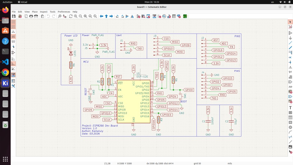
The completed schematic for this project shows the full ESP8266 development board. The design is organized into clearly labeled blocks:
- Power LED block — a simple LED indicator with current-limiting resistor connected to the 3.3V rail, giving visual confirmation that the board is powered
- Power / PWR_FLAG block — contains the power connector J5 and PWR_FLAG symbols, which are required by KiCad's ERC to acknowledge that power is being properly sourced into the schematic
- UART block — connector J1 with RXD and TXD lines for serial communication, used for both programming the ESP8266 and for debugging output during development
- MCU block — the central ESP-12E module U1 with all its pins connected: RST, EN, ADC, CSO, MISO, GPIO0–GPIO16, TXD, RXD, VCC, GND, and SCLK/MOSI/MISO for SPI
- J3 SPI connector — a 6-pin header exposing the SPI bus (CSO, MISO, MOSI, SCLK) plus 3.3V and GND for connecting external SPI peripherals like displays, memory chips, or sensors
- J2 and J4 PIN headers — two 8-pin headers breaking out all the GPIO pins for easy access on a breadboard or for connecting external circuits
- Decoupling capacitors C1 and C2 — 100nF capacitors placed directly on the power pins of the ESP-12E to filter high-frequency noise and prevent voltage glitches during Wi-Fi transmission (the ESP8266 draws significant current spikes during RF activity)
- Pull-up resistors R1–R5 — 10kΩ resistors on EN, GPIO0, GPIO2, and GPIO15 to establish correct boot conditions for the ESP8266
Understanding the ESP8266 Boot Conditions
A critical aspect of designing with the ESP8266 that affects the schematic is the boot mode selection. The ESP8266 checks the state of certain GPIO pins at power-up to determine which boot mode to enter:
- GPIO0 must be HIGH (pulled up) for normal operation. If GPIO0 is LOW at boot, the chip enters flash download mode, waiting for firmware over UART.
- GPIO2 must be HIGH at boot.
- GPIO15 must be LOW at boot.
- EN (chip enable) must be HIGH to enable the chip.
- RST must be HIGH for normal operation.
This is why the schematic includes pull-up resistors on EN and GPIO0, and a pull-down resistor on GPIO15. The reset button (SW) connects RST to GND through a small debounce resistor — pressing it briefly resets the chip. For programming mode, GPIO0 is also connected to a button (labeled BOOT/SW1) so you can hold GPIO0 low during reset to enter flash mode.
Essential Schematic Tools
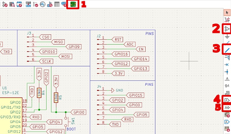
The KiCad schematic editor has many tools, but five are used in virtually every design. Understanding these tools deeply is what separates a slow, frustrating schematic drawing session from a smooth, efficient one.
1. Add Symbol (keyboard shortcut: A)
This is the gateway to placing any component into your schematic. Pressing A opens the "Choose Symbol" dialog — a searchable browser of all loaded symbol libraries. You can search by component name, part number, description, or keyword. The dialog shows a preview of the selected symbol with all its pins labeled, the default footprint, and a link to the datasheet if available.
When you place a symbol, KiCad automatically assigns it a reference designator (R1 for resistors, C1 for capacitors, U1 for ICs, J1 for connectors, etc.). You can also place the same symbol multiple times in sequence if you need many identical components. Each placed symbol represents one real component on your board.
2. Add Wire (keyboard shortcut: W)
Wires are the fundamental connections in a schematic. Press W and click to start drawing a wire, then click again to end it. Wires automatically connect when they touch pin endpoints or other wires at T-junctions. KiCad draws wires in horizontal and vertical segments by default, though you can switch to 45° mode.
Understanding what makes a valid connection in KiCad is important: two wires simply crossing each other are NOT connected — a junction dot must be placed explicitly. However, if a wire ends exactly at the end of another wire or at a pin, they are connected. This strict rule prevents accidental short circuits and makes schematics unambiguous.
3. Add Net Label (keyboard shortcut: L)
Net labels are one of the most powerful schematic tools. A net label is a named tag attached to a wire. Any two wires anywhere on the schematic that share the same label name are electrically connected, as if you had drawn a wire directly between them.
This is essential for keeping schematics readable. Without net labels, you would need to draw long wires across the entire schematic to connect a microcontroller's TX pin to a UART connector — cluttering the schematic with crossing wires that make it hard to read. With net labels, you simply label the MCU's TX pin TXD and label the corresponding pin on the connector TXD, and KiCad knows they are connected. The schematic stays clean and organized.
In this design, net labels are used extensively: TXD, RXD, GPIO00 through GPIO16, RST, EN, ADC, MOSI, MISO, SCLK, CSO, and power nets 3.3V and GND.
4. Add Power Port
Power symbols are special global net labels specifically for power nets. When you place a GND symbol, it is automatically connected to every other GND symbol on every sheet of your schematic. The same applies to 3.3V, VCC, +5V, or any other power symbol.
Power symbols serve two purposes: they provide a clean visual way to show power connections without drawing wires everywhere, and they allow KiCad's ERC to verify that power is properly defined and connected. The PWR_FLAG symbol is a special power symbol that you must place on any power net that is sourced from a connector — it tells the ERC "yes, this net is intentionally powered from outside the schematic."
5. Add No Connect (keyboard shortcut: Q)
The No Connect marker is a small X that you place on pins that are intentionally left unconnected. This is crucial for the ERC (Electrical Rules Check). If a pin has no wire, no label, and no No Connect marker, the ERC flags it as an error because an unconnected pin could indicate a mistake.
For the ESP-12E, which has many GPIO pins, several pins may not be used in a given design. Placing No Connect markers on unused pins tells KiCad "I know this pin is unconnected, I did this intentionally, do not warn me about it." A clean ERC with zero errors or warnings is the goal before moving to PCB layout.
Placing the ESP-12E Module
The heart of this board is the ESP-12E module, which houses the ESP8266EX SoC along with 4MB of flash memory, a PCB antenna, and all the supporting circuitry in a small 24×16mm shielded module.
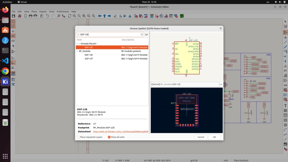
Searching for ESP-12E in the symbol chooser reveals the component under the RF_Module library. The "Already Placed" section at the top of the list shows that an ESP-12E has already been placed in this schematic — this is helpful when you need to place multiple instances or want to verify you are using the same symbol.
The symbol preview on the right shows all 22 pins of the ESP-12E: - RST — active-low reset pin - EN — chip enable, must be HIGH for operation - ADC — single 10-bit analog-to-digital converter input (0–1V range) - GPIO0–GPIO16 — general purpose I/O pins (not all numbers exist in the ESP8266) - TXD / RXD — UART0 transmit and receive (also GPIO1 and GPIO3) - SCLK / MOSI / MISO / CSO — SPI bus pins (also GPIO14, GPIO13, GPIO12, GPIO15) - VCC — 3.3V power supply - GND — ground (multiple pins)
The footprint RF_Module:ESP-12E is pre-assigned, which is the correct physical footprint for the castellated-edge pads of the ESP-12E module. When this symbol is synchronized to the PCB editor, the correct 22-pad footprint with the keep-out zone for the antenna area is automatically used.
Using Fab Library Components
For passive components (resistors, capacitors) and connectors, I exclusively used components from the PCM_fab library to ensure compatibility with Fab Lab inventory.
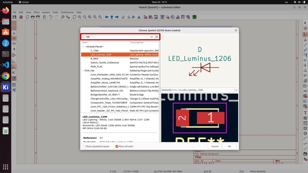
Searching for fab in the symbol chooser filters the results to show the PCM_fab library. The components visible include:
- LED_Luminus_1206 — a 1206 package white LED (Cool 5000K, 2.85V forward voltage, 60mA), used for the power indicator LED in this design
- R_0603 — standard 0603 package resistor, used for all pull-up and current-limiting resistors
- C_1206 — 1206 package capacitor for the decoupling capacitors
- Switch_Tactile_CUIDevices — a tactile push button for the reset and boot switches
- PWR_FLAG — the special power flag symbol described earlier
- Conn_PinHeader_UPDI_2x03_P2.54mm — a 6-pin 2.54mm pitch connector for the SPI header
- Conn_Header_JST_PH_1x02_P2mm — a 2-pin JST PH connector for the power input
Using these specific components is important for two reasons. First, the footprints are guaranteed to match the actual components in the Fab Lab — so when you mill your board and go to solder components, everything will fit correctly. Second, the component values and package sizes are what Fab Labs typically stock, so you can actually build your design without needing to order anything special.
PCB Editor — Physical Layout
Once the schematic is fully connected and passes ERC with zero errors, it is time to move to the PCB Editor to create the physical board.
The transition happens via Tools → Update PCB from Schematic (shortcut: F8). This imports all footprints from the schematic into the PCB editor and establishes the ratsnest — the thin lines showing which pads need to be connected by copper traces. Initially, all footprints are stacked on top of each other and need to be separated and arranged.
The completed PCB layout shows all components placed and all traces routed on the F.Cu (front copper) layer. The design process involves several phases:
Component Placement is the most important phase — getting good placement is the foundation of a good PCB. The ESP-12E module goes in the center because it is the largest component and everything else connects to it. The GPIO headers go on the right side where they are accessible for breadboard connections. The programming/UART connector goes on the bottom edge for easy access. Decoupling capacitors go as close as possible to the power pins they filter — this is critical for their effectiveness. Bypass capacitors more than a few mm away from their target pins are much less effective at filtering high-frequency noise.
Board Outline is drawn on the Edge.Cuts layer to define the physical boundary of the board. Everything must fit within this boundary, and components should have their courtyard boundaries (the keep-out zone around each footprint) entirely within the board edge.
Trace Routing connects the component pads following the ratsnest connections. You must choose appropriate trace widths: signal traces (GPIO, UART, SPI) can be as thin as 0.25mm, while power traces (3.3V, GND) should be wider (0.8–1.0mm or more) to carry current without excessive resistance.
Copper Pour adds a ground plane that covers the entire board — significantly improving signal integrity and reducing EMI.
PCB Editor Tools
The PCB editor has a rich set of tools. The six most frequently used are:
1. Highlight Net
Clicking any copper element while in this mode highlights the entire net it belongs to — all traces, pads, and zones that share that electrical connection glow brightly. This is invaluable for visually verifying your routing. After routing a complex board, it is good practice to click every net and visually confirm it connects the correct pads. A misrouted trace where the wrong pads are connected is a serious error that is much easier to catch visually than to debug later on a physical board.
2. Route Single Track (X)
This is the primary routing tool and the one you will spend the most time with. Press X, click a pad to begin routing, move the cursor to the destination pad, and click to complete the trace. KiCad's interactive router is highly intelligent — it can push other traces out of the way (in Push and Shove mode), walk around obstacles, and automatically complete connections while respecting design rules.
The track width used while routing is set in the toolbar at the top of the screen. You can define multiple preset widths and switch between them. A good practice is to set up presets for signal traces (0.25mm or 0.5mm), power traces (1.0mm), and wide power (2.0mm) before starting to route.
3. Interactive Router Settings
This tool switches between three routing modes: - Highlight Collision: shows violations but does not prevent you from routing through them - Push and Shove: automatically moves existing traces to make room for the new trace being routed — very fast for dense boards - Walk Around: the router finds a path around obstacles without moving them — more conservative but produces cleaner results
For this design, Walk Around mode was used to maintain clean, predictable trace paths.
4. Add Copper Zone (Ctrl+Shift+Z)
A copper zone (also called a copper pour or ground plane) is a filled polygon of copper on a layer assigned to a specific net. For PCBs, a ground plane on the entire board is almost always a good idea. It provides: - A low-impedance return path for all signals - Reduced EMI radiation since return currents flow directly beneath their signal traces - Better heat dissipation across the board - Mechanical strength (more copper = stiffer board) - Reduced unrouted connections since many components need GND connections which the pour handles automatically
After drawing the zone boundary, press B to fill all zones. Press B again after any routing changes to update the fill.
5. Add Line
Draws graphical lines on any layer. Primary use is drawing on Edge.Cuts for board outlines, silkscreen annotations, or courtyard boundaries. Unlike traces (which carry electrical signals), lines are purely graphical and carry no net assignment.
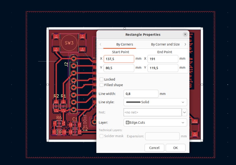
6. Add Rectangle
Draws a filled or outline rectangle on any layer. I used this to draw the board outline on Edge.Cuts by entering exact corner coordinates in the properties dialog, giving a precise rectangular board shape.
Defining the Board Outline
The board outline is defined on the Edge.Cuts layer. This layer is special — KiCad uses it to know where to cut the board during fabrication (either with a milling machine or a router). Everything on Edge.Cuts must form a complete, closed boundary with no gaps.
Using the rectangle tool and opening its properties dialog (press E after placing), I entered the exact corner coordinates:
| Property | Value |
|---|---|
| Start X | 137.5 mm |
| Start Y | 80.5 mm |
| End X | 191.0 mm |
| End Y | 119.5 mm |
| Board Width | 53.5 mm |
| Board Height | 39.0 mm |
| Layer | Edge.Cuts |
| Line width | 0.8 mm |
This produces a 53.5 × 39 mm board — a compact size that comfortably fits the ESP-12E module (24×16mm), all the pin headers, and supporting components with reasonable spacing between them. The board area is 20.865 cm², well within the capabilities of the Fab Lab milling machine and comfortably below the Eagle free-tier 80 cm² limit (though we are using KiCad where this does not matter).
When entering board dimensions, always add some margin around your component layout. Components should not be placed right at the board edge — leaving at least 1–2mm of clearance from the edge ensures that the milling process does not damage pads near the boundary, and gives the board a clean professional appearance.
Adding a GND Copper Fill
To improve signal integrity, reduce electromagnetic interference, and simplify routing (since most components need a GND connection), I added a copper fill zone connected to the GND net covering the entire board on the F.Cu layer.
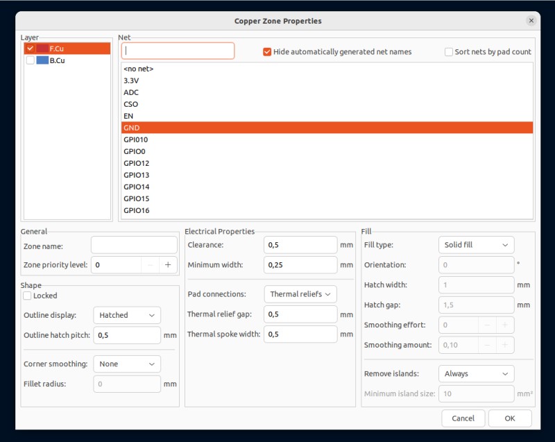
The Copper Zone Properties dialog has many configurable parameters. Here is what each setting means and why I chose these values:
Layer — F.Cu: The fill is on the front copper layer, which is the same layer where all the traces are routed in this single-layer design. You could also add a fill on B.Cu for a back-side ground plane on a two-layer board.
Net — GND: The fill is assigned to the GND net. All pads connected to GND will connect to this fill directly (or through thermal relief spokes). The net list shows all available nets in this design: 3.3V, ADC, CSO, EN, GPIO0–GPIO16, GND, MISO, MOSI, RST, RXD, SCLK, TXD.
Pad connections — Thermal reliefs: Instead of connecting pads directly to the copper fill (which would create a massive heat sink), thermal reliefs create four thin copper spokes connecting the pad to the fill. This is crucial for hand soldering — a pad directly connected to a large copper plane dissipates heat so quickly that it is nearly impossible to reach soldering temperature with a normal iron. Thermal reliefs solve this problem. The thermal relief gap (0.5mm) and spoke width (0.5mm) are standard values that work well.
Clearance — 0.5mm: The minimum gap between the GND fill and any other net's copper. This prevents shorts between the fill and signal traces. 0.5mm is a safe value for FR4 PCBs — the standard clearance for 50V and below with most manufacturers.
Minimum width — 0.25mm: The thinnest copper feature that will be generated within the fill. Small areas between closely-spaced pads might produce narrow copper slivers — this setting ensures they are at least 0.25mm wide.
Fill type — Solid fill: The entire zone area is filled with solid copper, as opposed to hatched fill (a grid pattern). Solid fill provides better electrical performance. Hatched fill is sometimes used for mechanical flexibility or weight reduction but is rarely needed for standard PCBs.
Remove islands — Always: Copper islands are isolated fragments of the fill that have no electrical connection to the rest of the GND net (disconnected by surrounding traces). These islands are noise antennas and serve no useful purpose, so they are automatically removed.
After configuring all these settings and drawing the zone boundary around the board perimeter, pressing B fills the entire available area with copper, automatically connecting to all GND pads.
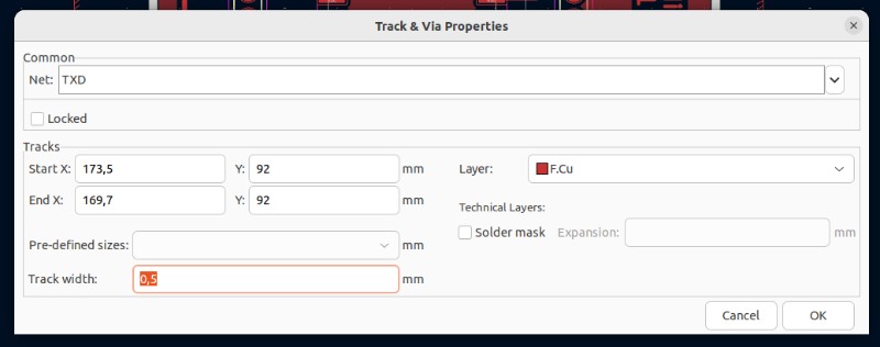
Track and Via Properties
Individual tracks were verified and adjusted using the Track & Via Properties dialog. This allows precise control over every aspect of a trace.
Examining the TXD signal trace reveals:
| Property | Value |
|---|---|
| Net | TXD |
| Layer | F.Cu |
| Track width | 0.5 mm |
| Start | X: 173.5mm, Y: 92mm |
| End | X: 169.7mm, Y: 92mm |
| Length | ~3.8 mm |
A width of 0.5 mm was chosen for all signal traces in this design. The general rule for trace width selection is based on the current the trace needs to carry:
- 0.2–0.25 mm: Minimum width, suitable for very low-current signals (< 100mA). Challenging for in-lab CNC milling.
- 0.5 mm: Good general-purpose signal trace width. Carries up to ~500mA, easy to mill, good for GPIO and communication signals.
- 1.0 mm: Power traces carrying 1A or more. Used for the 3.3V supply traces in this design.
- 2.0 mm and wider: High-current power distribution. Not needed for this low-power ESP8266 board.
For the ESP8266, which draws peaks of up to 400mA during Wi-Fi transmission, the 3.3V supply traces were made wider (1.0mm) while all signal traces (GPIO, UART, SPI) use 0.5mm width. This provides adequate current capacity with a comfortable safety margin.
Final PCB
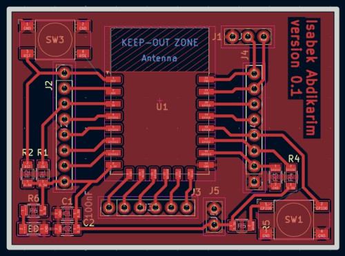
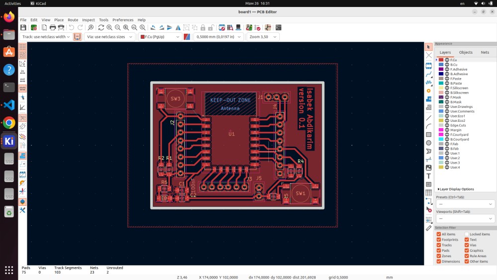
The completed board displays the full design with the GND copper pour filled across the front copper layer. The dark areas between pads and traces show the GND copper fill, while the lighter areas show where the copper has been cleared away (the solder mask openings over pads and the trace routing channels).
The final board includes all the following elements working together:
ESP-12E Module (U1): Centered on the board with its antenna keep-out zone (the rectangular outline marked with hatching in the upper portion of the module area). No copper, components, or traces are allowed within this zone as they would interfere with the antenna's radiation pattern and degrade Wi-Fi performance. The module has castellated pads (half-circles along its edges) that solder to the pads on the main board.
GPIO Headers J2 and J4: Two 8-pin 2.54mm pitch headers on the right side of the board, each breaking out a set of GPIO pins. The 2.54mm (0.1 inch) pitch is the standard breadboard pitch, making this board directly pluggable into a standard breadboard for prototyping.
SPI Header J3: A 6-pin header on the upper left exposing the full SPI bus (MOSI, MISO, SCLK, CSO) plus power (3.3V, GND). Used for connecting SPI peripherals such as OLED displays, SD card modules, or ADC/DAC chips.
UART Header J1: A 4-pin header on the left side for serial communication. During development, this connects to a USB-UART adapter for programming the ESP8266 and reading serial debug output. The pinout matches the standard FTDI cable pinout (GND, VCC, RXD, TXD).
Reset Button SW3 and Boot Button SW1: Two tactile push buttons in the upper-left and lower-right corners respectively. SW3 resets the chip, SW1 (labeled BOOT) holds GPIO0 low for entering flash programming mode. The standard programming procedure is: hold SW1, press and release SW3, release SW1 — this enters firmware upload mode.
Pull-up Resistors R1–R5: Five 10kΩ 0603 resistors ensuring correct boot states on EN, GPIO0, GPIO2, and other control lines.
Decoupling Capacitors C1 and C2: Two 100nF 1206 capacitors placed directly adjacent to the power pins of the ESP-12E. Their close proximity to the VCC pins ensures they effectively filter the current spikes from Wi-Fi activity.
Power LED (D) with Resistor R6: An LED indicator connected between 3.3V and GND through a current-limiting resistor (330Ω for approximately 10mA at 3.3V with a 2.0V forward voltage LED). Lights up whenever the board is powered.
Silkscreen Text: The board includes author information (Isabek Abdikarim), version number (0.1), and component reference designators on the silkscreen layer, making the board easy to assemble and identify.
Design Rules Check (DRC)
Before considering a PCB design complete, always run the Design Rules Check (DRC) (under Inspect menu). The DRC verifies that:
- No copper features are closer together than the minimum clearance (prevents shorts)
- All trace widths meet the minimum width requirement (prevents open circuits during fabrication)
- No courtyard overlaps between components (prevents assembly conflicts)
- All pads are within the board boundary
- No unconnected nets remain (all ratsnest connections have been routed)
- No drill violations (via or hole diameters within allowed range)
A clean DRC with zero errors is mandatory before sending designs for fabrication. Any DRC error represents either a potential manufacturing defect or an assembly problem that will cause the board to fail.
Exporting for Fabrication
With the design complete and DRC passing cleanly, the final step is exporting the manufacturing files:
Gerber files are the industry-standard format for PCB fabrication. They are a set of files — one per layer — that tell the manufacturer exactly where to put copper (F.Cu.gbr, B.Cu.gbr), where to apply solder mask (F.Mask.gbr, B.Mask.gbr), where to print silkscreen (F.Silkscreen.gbr), and where to cut the board outline (Edge.Cuts.gbr). In KiCad, Gerbers are exported via File → Fabrication Outputs → Gerbers.
Drill files (.drl) specify the location and diameter of every hole on the board — component through-holes, mounting holes, and vias.
For in-lab CNC milling, KiCad can also export SVG or DXF files of individual layers, or you can use tools like FlatCAM to process the Gerber files directly into G-code for the milling machine.
Conclusion
This week's electronics design work resulted in a fully designed, DRC-clean ESP8266 development board that demonstrates the complete KiCad PCB design workflow. Starting from an empty project and ending with a manufacturable board design, every step of the process was covered: library setup, schematic capture, net labeling, footprint assignment, board outline definition, component placement, trace routing, copper pour, and design rule verification.
The most valuable lessons from this week's work:
Schematic first, PCB second — always: The schematic is the foundation of every PCB design. Time spent making the schematic clean, well-organized, and error-free pays dividends when moving to the PCB editor. A confusing schematic leads to routing mistakes; a clear schematic makes the PCB almost design itself.
Component placement is more important than routing: A good component placement makes routing straightforward. A poor placement makes routing a nightmare. Spend at least as much time on placement as on routing — cluster components by function, keep decoupling capacitors close to their power pins, and think about signal flow from input to output.
Net labels are your friend: Use them liberally. A schematic with clean net labels and no crossing wires is immediately understandable. A schematic with wires snaking in every direction is a source of errors.
Always add a ground pour: For almost every PCB design, adding a GND copper pour costs you nothing and improves the board significantly. Reduced EMI, simpler routing, better heat distribution, and improved signal return paths all come for free.
Use the official Fab library: The PCM_fab library exists because the Fab Academy community has done the work of verifying footprints against actual components. Using it saves time and prevents assembly failures.
Run ERC and DRC before anything else: These automated checks catch mistakes that are invisible to the human eye. A zero-error ERC/DRC is the minimum bar for a design ready for fabrication.
KiCad 9.0 proved to be an excellent, professional-grade tool that handles everything from simple single-layer boards to complex multi-layer designs. Its deep integration with the Fab Academy workflow through the PCM_fab library, combined with being completely free and open-source, makes it the ideal choice for electronics design at every level from student to professional engineer.
Design Files
- board1.kicad_pro — KiCad project file
Project: ESP8266 Dev Board | Author: Abdikarim Kamaluly | Version: 0.1 | KiCad 9.0