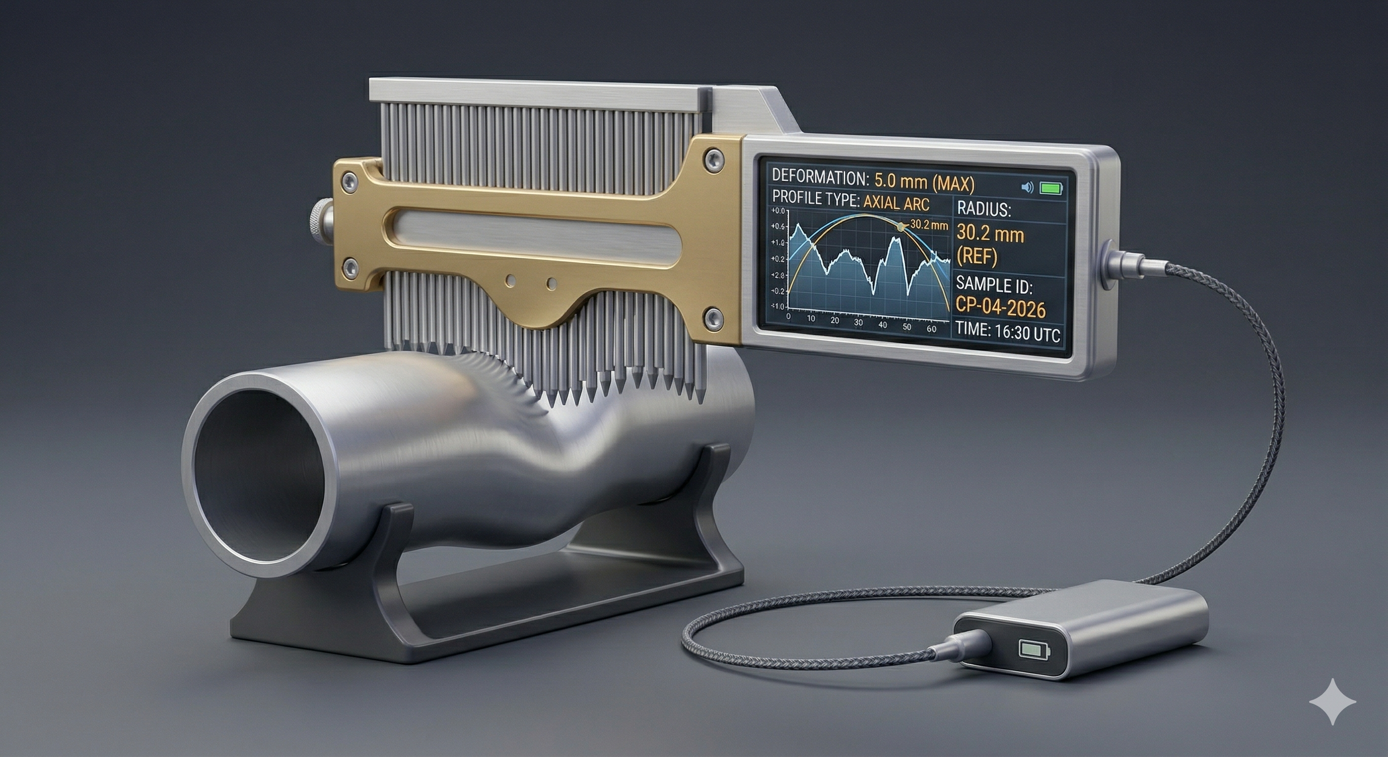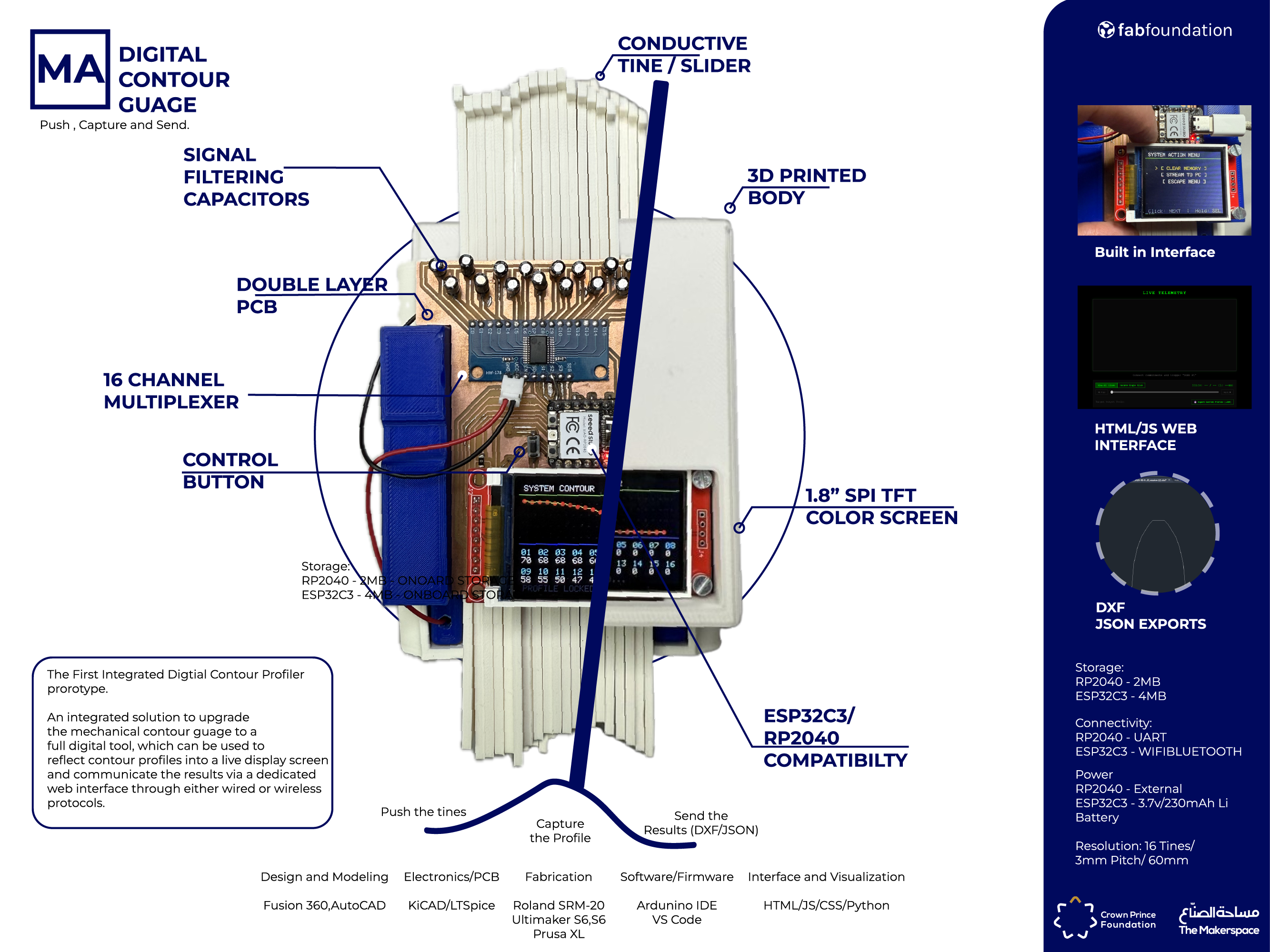
## Introduction ### Project Summary The Digital Contour Gauge (DCG) is a field-portable, open-source measurement instrument that digitally captures irregular surface profiles and cross-sections. Sixteen spring-loaded conductive tines slide across a Velostat resistive layer; their individual positions are multiplexed into a single ADC channel on a microcontroller, rendered as a real-time curve on a color TFT display, and exported as a DXF file for direct use in CAD software. The device is entirely self-contained, battery-powered, and fabricated from locally sourceable components and standard Fab Lab processes — 3D printing, PCB milling, and soldering.
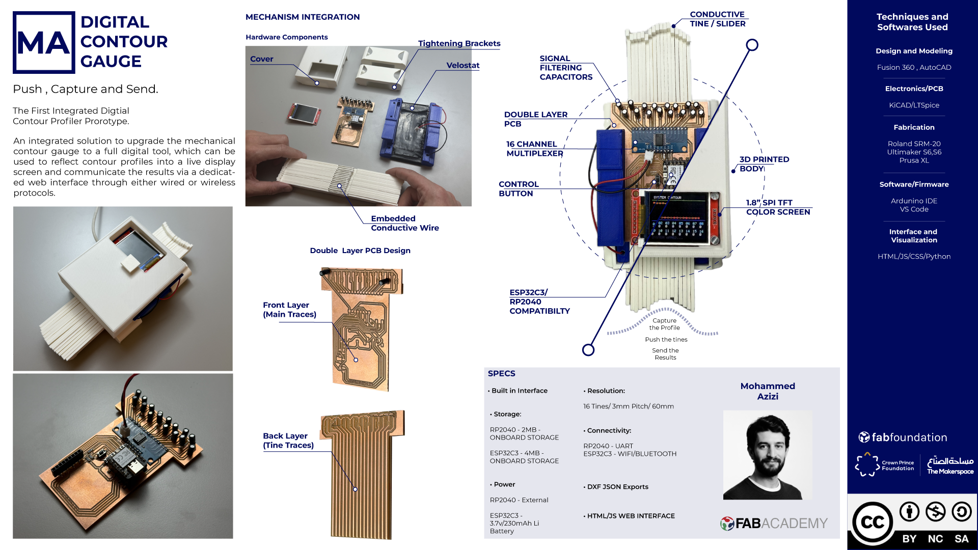
DCG Final Project Presentation Slide — 1920×1080 summary
Presentation slide — Fab Academy 2026 Final Review
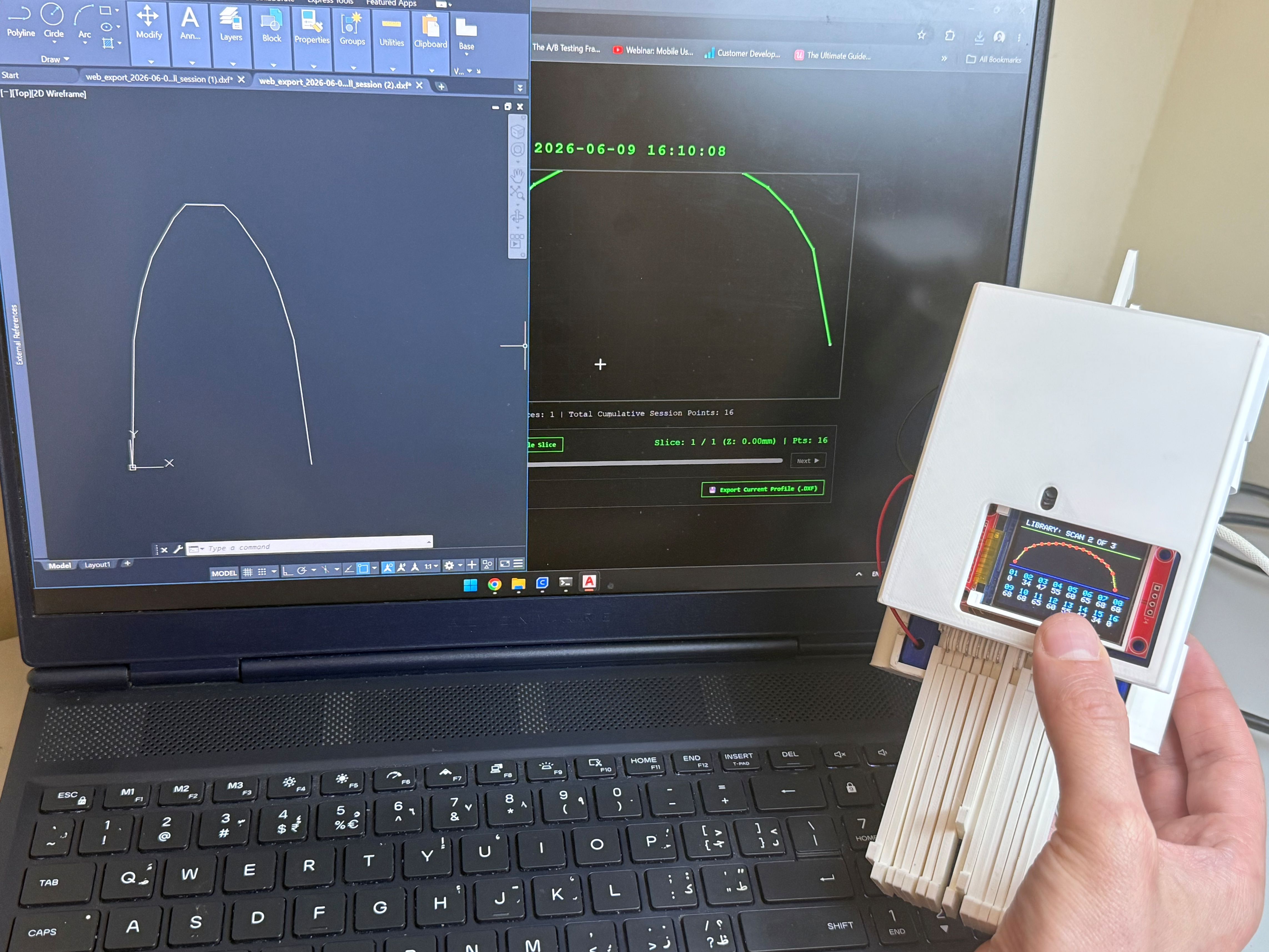
The assembled Digital Contour Gauge — final prototype
The assembled Digital Contour Gauge — final prototype (June 2026)
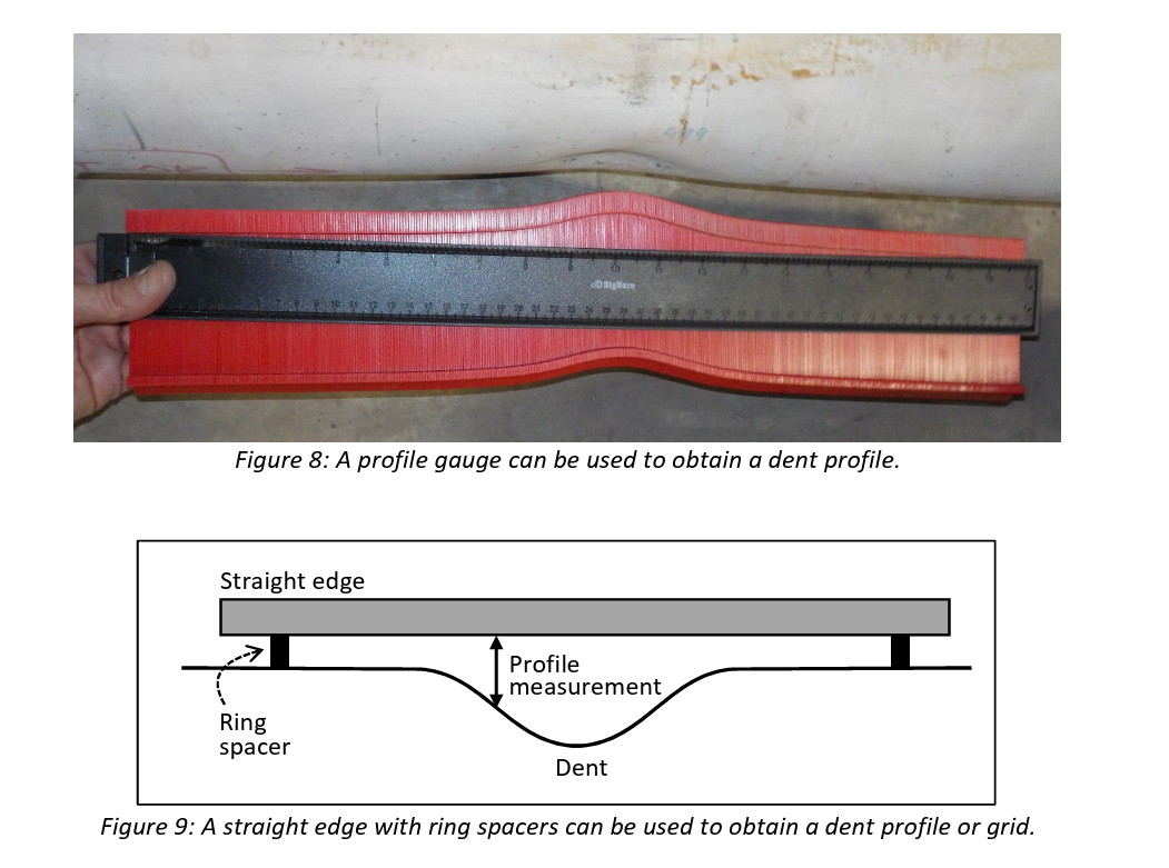
### The Problem During my work as a mechanical engineer on remote pipeline inspection sites, I frequently had to assess pipe deformations and dents against international standards — specifically ASME B31.8. In the field, access to digital measurement equipment was either impractical or unavailable. The workaround at the time was a manually operated mechanical contour profiler: effective, but slow, prone to transcription error, and impossible to digitally share or integrate into reports without redrawing everything by hand. The bottleneck was not the measurement concept — it was the complete absence of a digital pipeline between the physical gauge and the engineering report.
A manual contour gauge in use on a pipeline — field inspection context
Manual contour profiling on a pipeline — the field workflow this project replaces. ASME B31.8 Reference
### The Solution The inspiration for a digital version came directly from the ASME B31.8 dent strain assessment methodology, which at its core still relies on manual profiling. The logical step was to digitalize the tool itself: capture tine positions electronically, render them as a profile curve, and output the geometry as a standard CAD format. This increases accuracy, dramatically reduces workflow time, and makes results immediately shareable and printable in field reports.
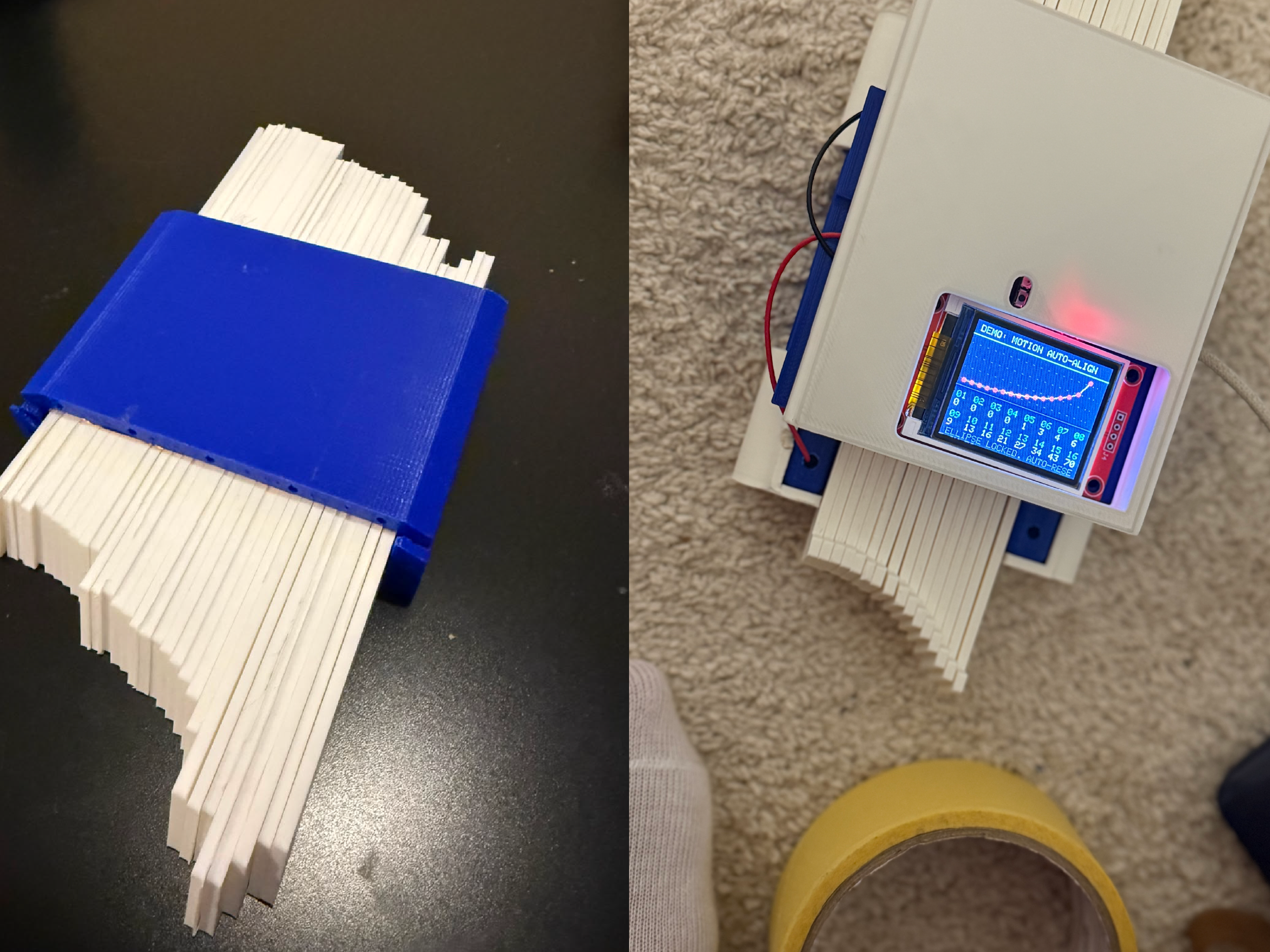
Traditional mechanical contour gauge (left) vs the Digital Contour Gauge (right)
Left: Traditional mechanical contour gauge. Right: Digital Contour Gauge (DCG) — same concept, fully digital output.
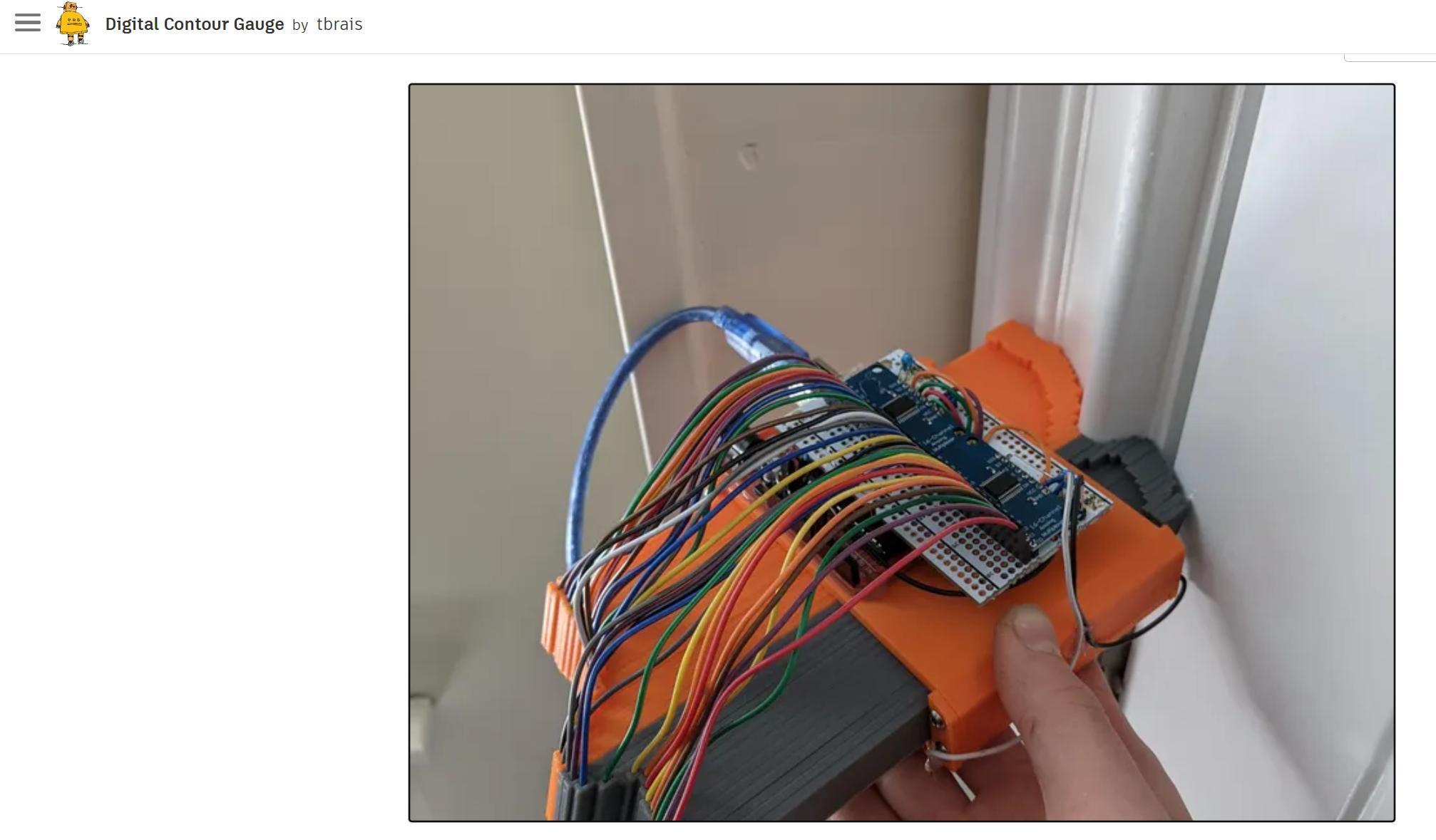
### Prior Art & Literature Review The mechanical contour gauge has existed in various forms for decades — different lengths, locking mechanisms, materials, and sizes — but all remain fully manual. The only documented attempt at a digital version is a project published on Instructables by user *tbrais*, which uses an Arduino Uno and a breadboard connected to Rhino/Grasshopper for visualization. That project, while conceptually valid, was never built into a complete integrated prototype. No field-ready, self-contained digital contour gauge with onboard display and CAD output exists in the public domain. This project fills that gap.
Screenshot of the tbrais Instructables digital contour gauge project — the only documented prior art
Prior art: the only documented digital contour gauge attempt, by tbrais on Instructables. Never completed as a full integrated prototype. View original

## Project Requirements & Success Criteria ### Design Constraints The project was engineered around the following self-imposed constraints from the outset: - All electronic components must be locally sourceable (sourced from MikroElektron, Amman, Jordan) - All structural components must be fabricable within a Fab Lab (3D printing, PCB milling) - The design must use minimal fasteners and eliminate threaded assemblies wherever possible - The system must be modular — individual tines replaceable without disassembling the electronics - The PCB must be compatible with both the Seeed Studio XIAO RP2040 and XIAO ESP32C3 without hardware changes - The device must be field-portable, running on a 3.7V LiPo battery ### Evaluation Criteria The project is considered successful when the following conditions are met: 1. The first assembly achieves high-quality manufacturing with a minimal number of fasteners and no dependency on external custom parts 2. The enclosure is rigid enough to absorb handling pressure and protect the electronics from damage 3. The design is reasonably modular with a plug-and-play tine replacement pathway 4. The device can be manufactured entirely from local materials given access to a double-layer PCB 5. The double-layer PCB concept is implemented in an actual functional use case 6. The interface is easy to read and use, with a working POC that can be scaled further
2.3 Scope Decisions — What Was Cut and Why
  • 32 tines → 16 tines: Reduced to manage PCB routing complexity and sensor array fabrication time within the project timeline. The 16-tine version provides sufficient spatial resolution for the primary use case.
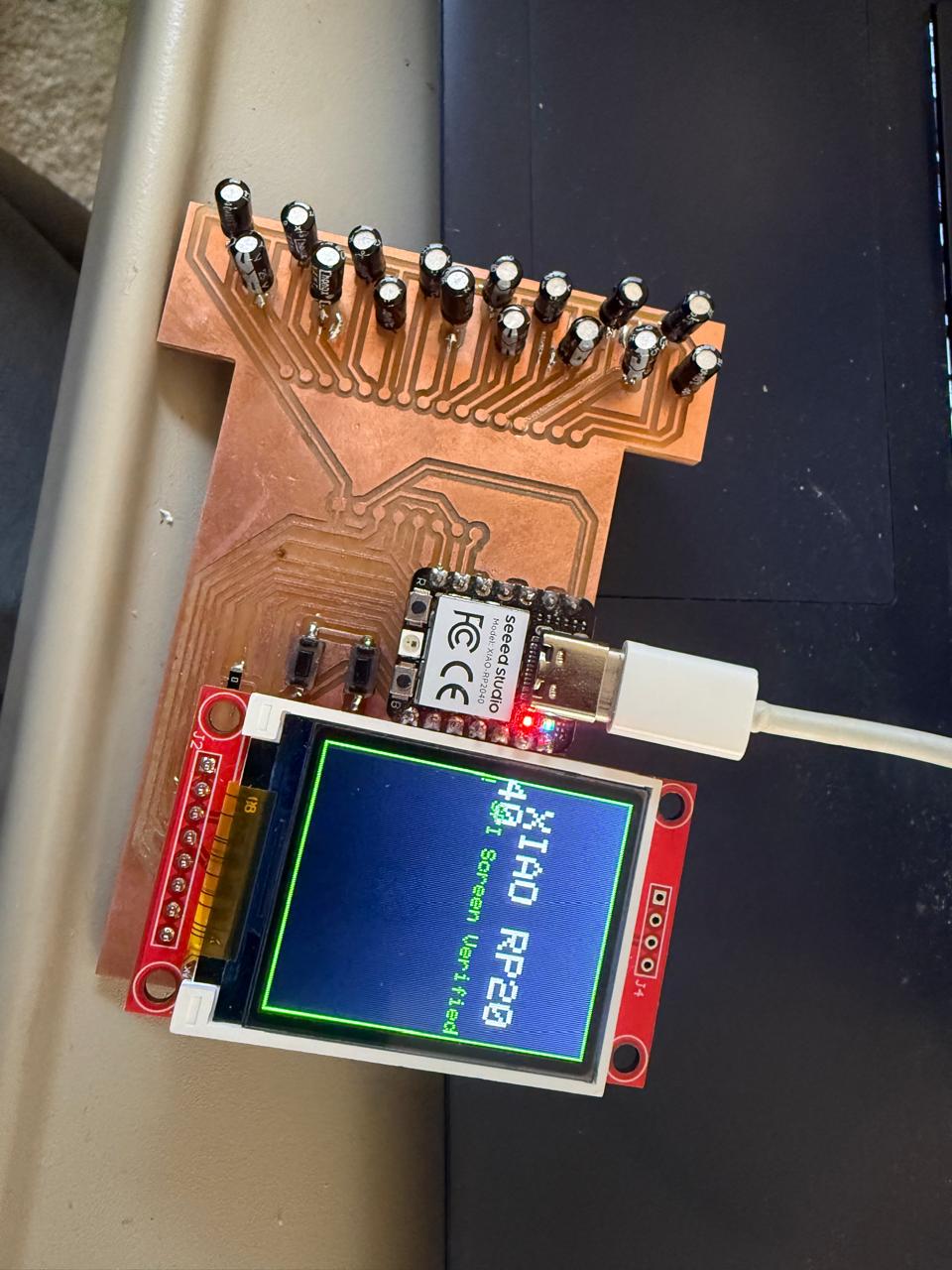
  • 4-pin OLED (SSD1306) → 7-pin SPI TFT color screen: The SSD1306 had a pin-swap issue between the physical module and the KiCAD footprint; the SPI TFT offered higher resolution and a cleaner interface for the final product.
  • Per-trace pull-down resistors → two shared resistors for tactile switches only: Simplified the PCB layout considerably. Multiplexer floating-gate protection was handled differently in the final firmware.
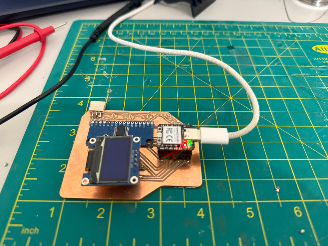
SSD1306 OLED module - old display choice
SSD1306 OLED (Left)
SPI TFT color screen - hardware display swap upgrade
SPI TFT color screen (Right) due to footprint pin-swap issue
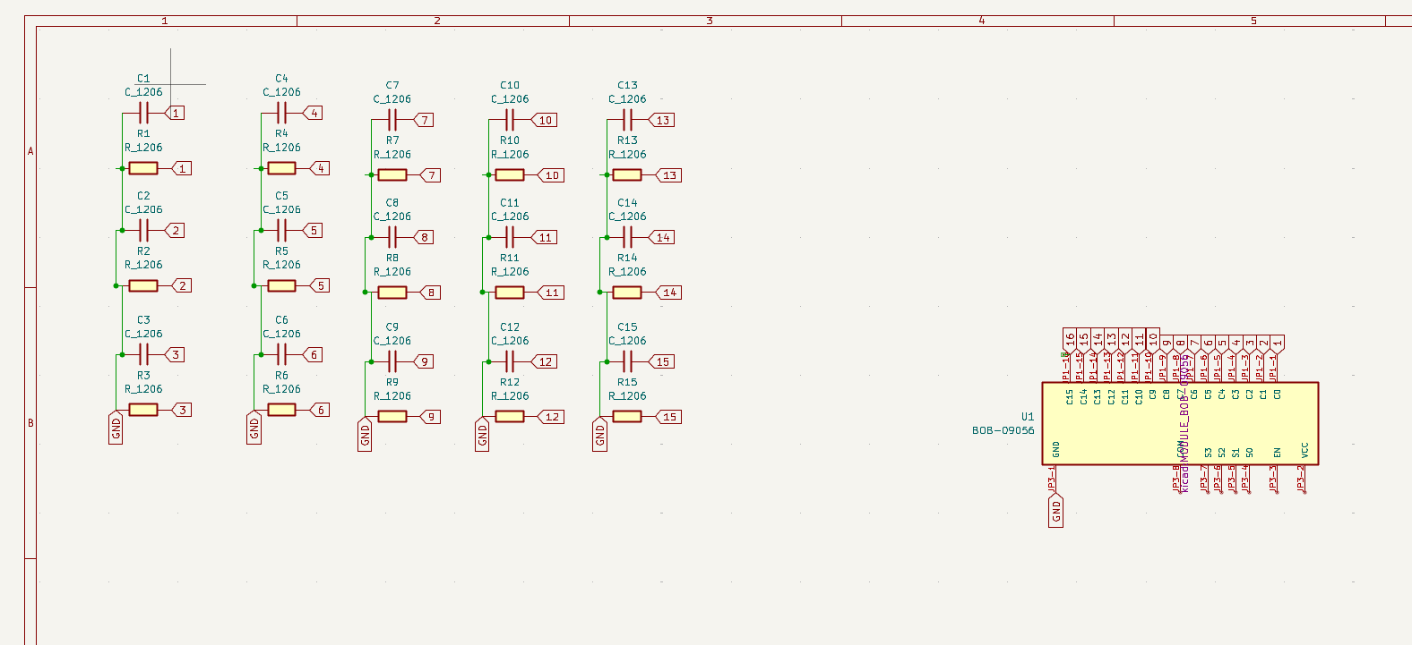
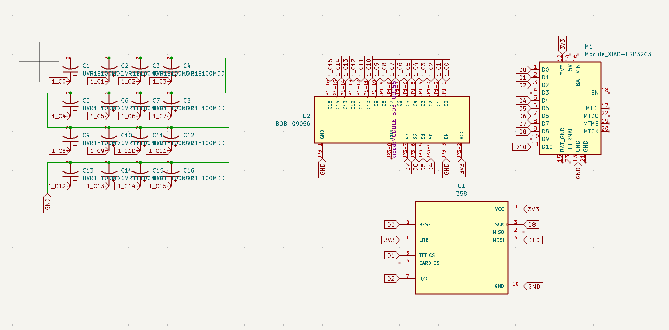
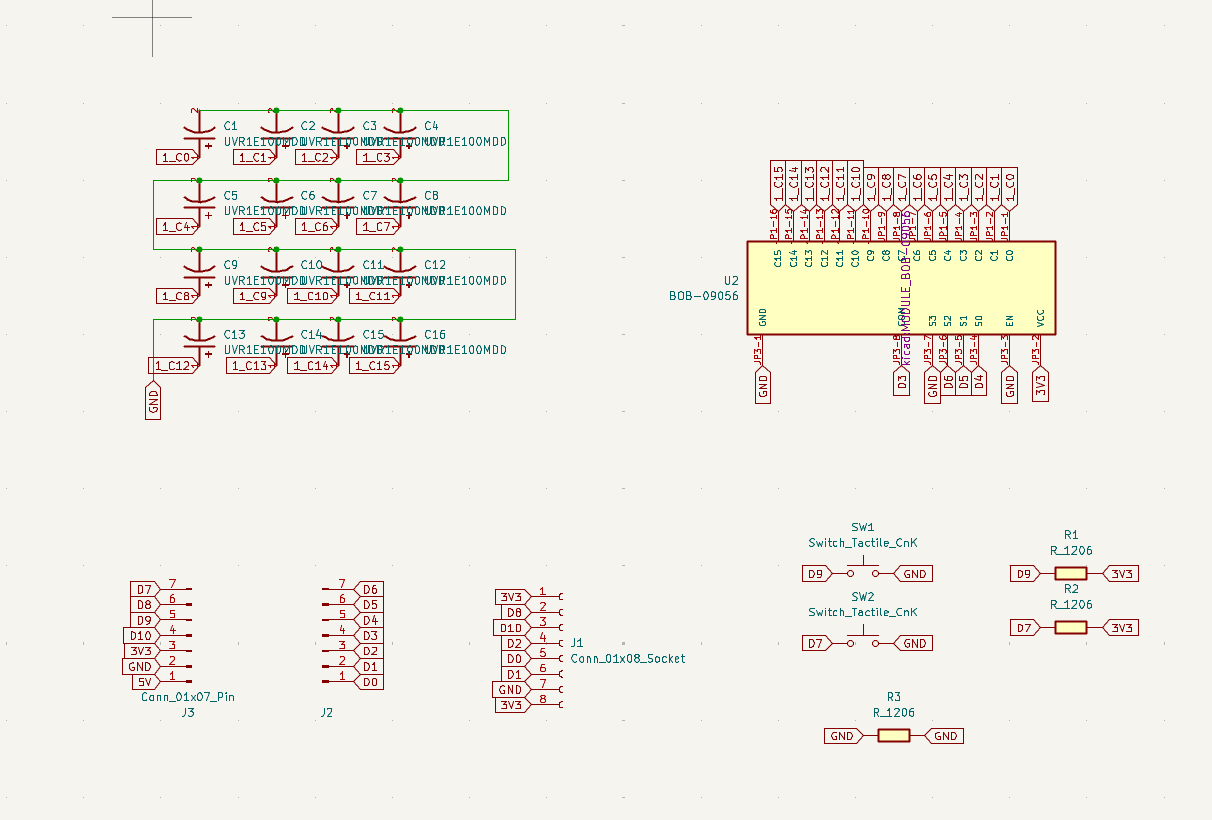
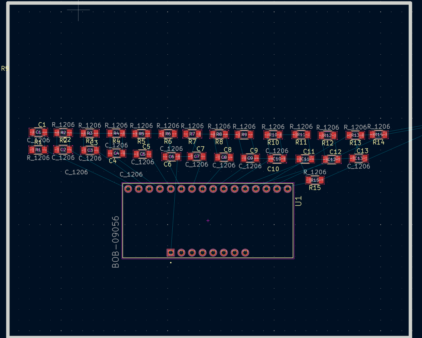
#### Schematic Diagram Progress
Initial Schematic Diagram
Second Schematic Diagram
Final Schematic Diagram
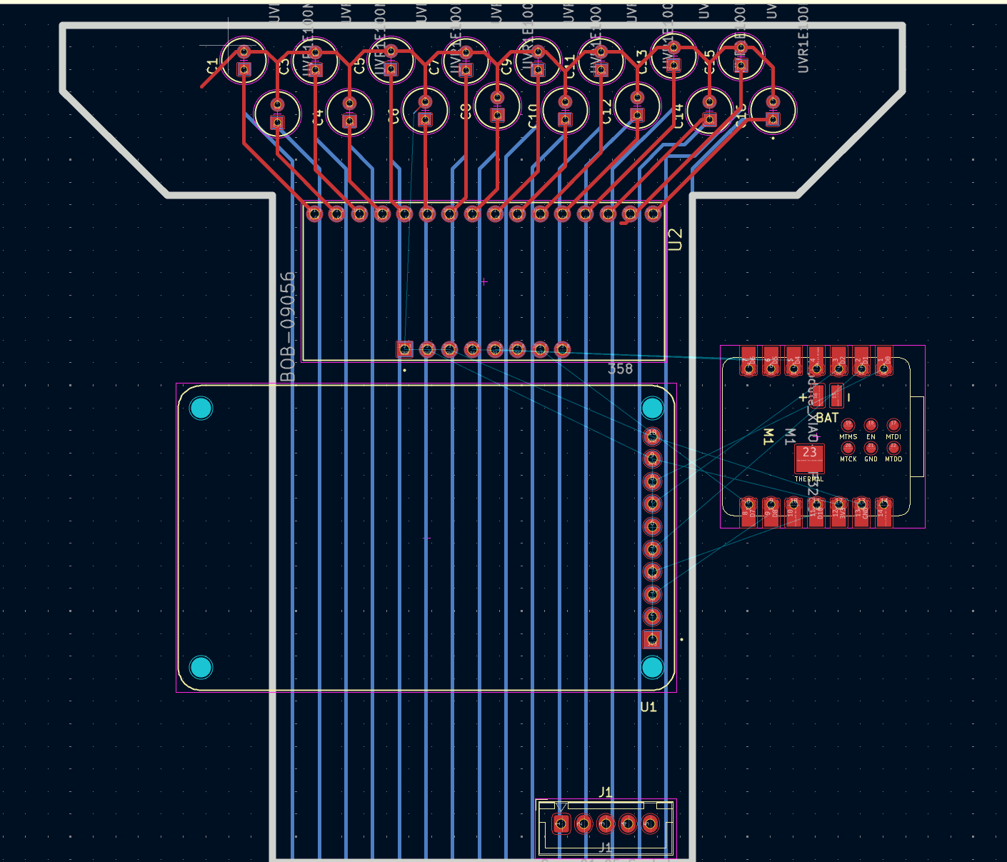
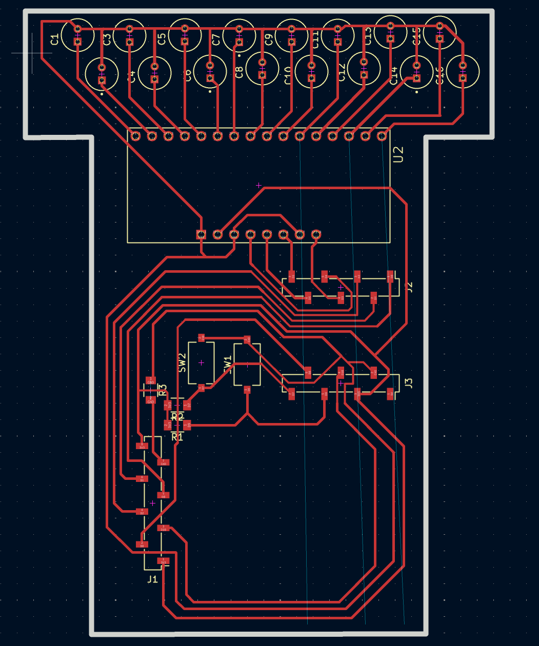
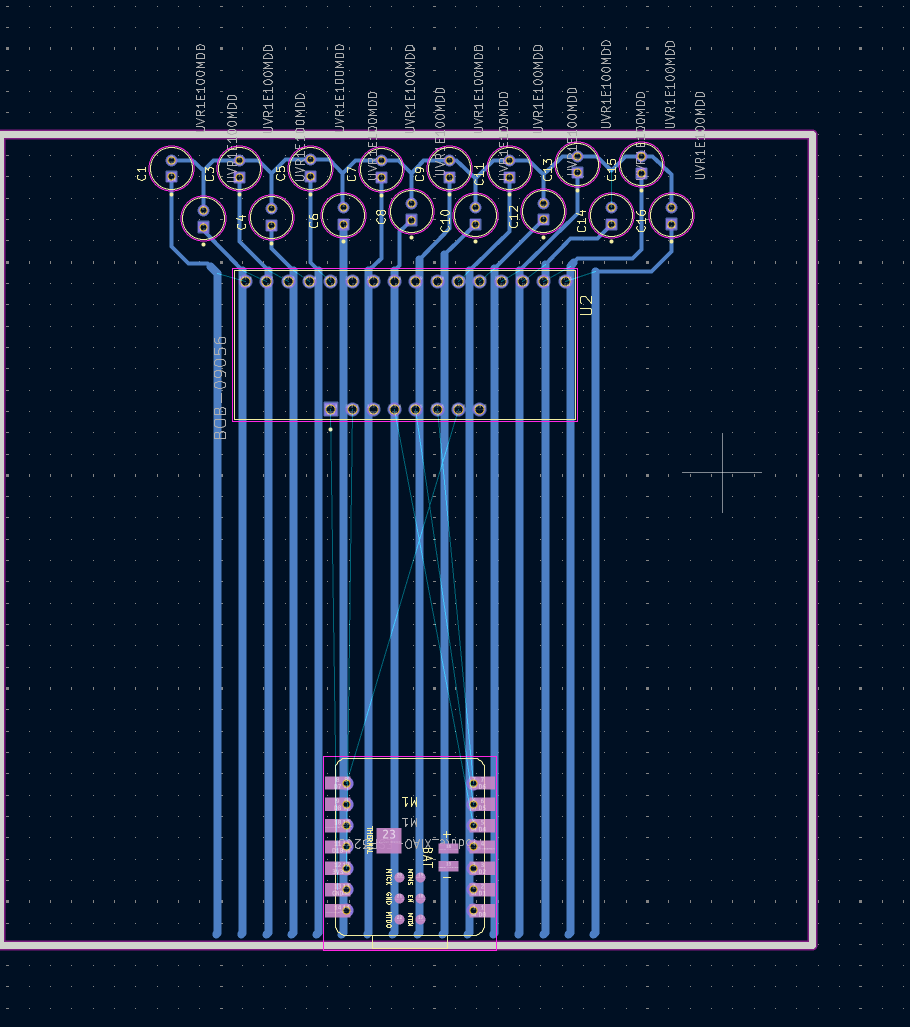
#### PCB Layout Progress
Initial PCB layout trace routing
Initial PCB Layout
Second iteration of PCB routing layout
Second PCB Iteration
Final PCB design - Front copper layer
Final PCB Layout (Front)
Final PCB design - Back copper layer
Final PCB Layout (Back)

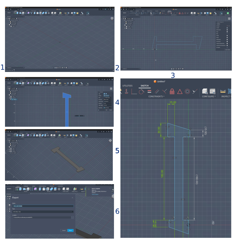
## Design Evolution ### Decision Matrix (Week 1) The DCG was selected over the original auto-feeder concept after a structured evaluation across three criteria: system integration potential, scalability, and direct real-world application. The auto-feeder was a simpler system; the contour gauge demanded electronics, firmware, mechanical design, and communications to work together — which aligned better with the Fab Academy scope and with the genuine engineering problem I had encountered in the field. *Full original proposal: [final-project-old.html](https://fabacademy.org/2026/labs/techworks/students/mohammed-azizi/final-project-old.html)* ### Concept Sketches & Early Modeling (Week 2) The first CAD work focused on modeling the tine — the individual sliding gauge pin — in both Fusion 360 and FreeCAD. This early modeling established the key dimensional constraints I will use when modelling the tine and allowed me to get familiar with sketching and iterating different tine geometries down the project and course, the references I had for different tine geometries from online searches and mainly falling back to the instructables design helped me to identify and imagine the geometry and dimensions of the tine, to which I decided to keep it 3mm thick , 120-150mm long with opposite lips from both ends chamfered at 30-60 degrees.
Early ai generated concept sketch of the digital contour gauge- part of the first week assignment
Week 2: Early concept sketch — tine geometry and enclosure layout.
First Fusion tine model — Week 2
Week 2: First Fusion tine model — establishing proportions and key dimensional constraints.
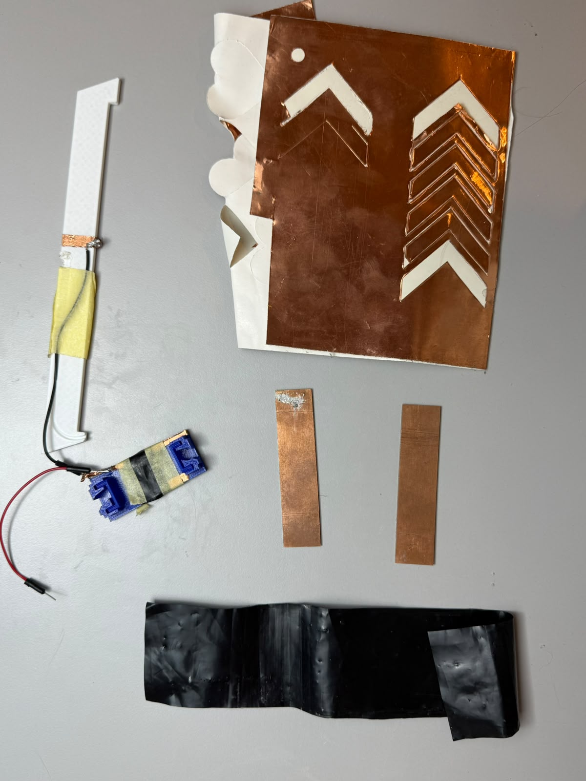
### Sensor & Actuator Ideation (Weeks 3–6) The central sensing question was: how do you convert a tine's linear position into an electrical signal? Several mechanisms were explored: - **Potentiometer (rotary):** Early concept, quickly discarded — no clean way to couple linear tine motion to a rotary element without significant mechanical complexity. - **Custom linear potentiometer (Velostat):** A sheet of Velostat conductive plastic, sandwiched between two copper busbars carrying VCC and GND, acts as a continuous resistive track. A tine with a conductive tip pressing against the Velostat at a specific position creates a voltage divider — the output voltage is proportional to position. This was the selected mechanism. - **Conductive PLA filament:** Investigated as an alternative tine material that would eliminate the need for separate wiper contacts. Rejected due to local unavailability, high internal resistance variability, and unacceptable experimental risk and cost. - **Copper tape busbars:** Tested as the voltage distribution rail along the Velostat edges. Confirmed viable and used in the final design. - **1mm conductive steel wire:** Adopted as the tine wiper tip, embedded into the 3D-printed tine body, providing a reliable low-resistance contact point against the Velostat layer.
Sensing material candidates: Velostat sheet, copper tape busbars, conductive steel wire, and conductive PLA sample
Sensing mechanism candidates evaluated — Velostat, copper tape busbars, conductive steel wire, and conductive PLA. Steel wire embedded in PLA was selected.
Diagram: Velostat voltage divider principle — VCC busbar, Velostat, GND busbar, tine wiper, FR1 trace, MCU ADC
Velostat voltage divider principle tine position determines output voltage. This is the core sensing mechanism of the DCG.
### The 7-Phase Design Plan (Week 6) Following the sensor selection, a structured 7-phase design plan was established to guide all subsequent work: 1. **Tine Design** — Individual gauge pin geometry and conductive integration 2. **Enclosure** — Main chassis dimensioning and internal architecture 3. **Mechanical Assembly** — Fitment testing and tolerance validation 4. **Electronic Placement** — KiCAD integration with physical envelope 5. **Mech/Elec Assembly** — Merging hardware and housing into a unified system 6. **BOM & Manufacturing** — Part lists and fabrication method confirmation 7. **Final Prototype** — Assembly, calibration, and documentation ### 3D Model Iterations (Weeks 2, 5, 15) The 3D model of the DCG evolved through three major versions: - **Benchmarking phase (Week 5):** Components from Thingiverse were printed in different PLA materials to understand tolerances, surface finish behavior, and spring-back characteristics relevant to the tine mechanism. - **DCG V1 (Week 15 preliminary):** First full enclosure model. Tines were integrated into fixed tracks; the design considered conductive filament as the track material before the Velostat approach was finalized. - **DCG V3 (Week 15 detailed):** The final design shape — multiple components and sub-assemblies, parametrically dimensioned around the KiCAD PCB layout.
Week 5 Instrucables benchmark prints — PLA material tolerance testing
Week 5: Instructable benchmark prints — testing PLA material tolerances, surface finish, and spring-back before committing to final tine geometry.
DCG V1 (Week 15 preliminary) — first full enclosure concept. Conductive filament was still the planned track material at this stage.

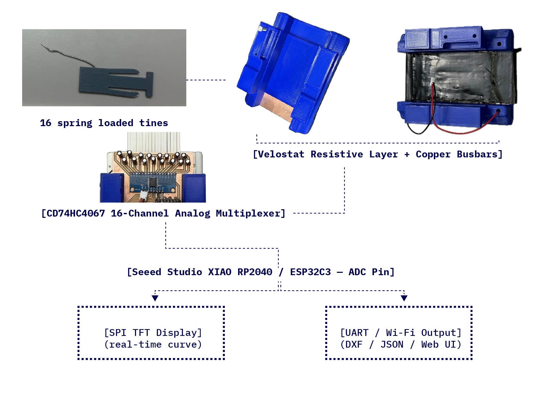
## Electronics Design & Production ### System Architecture The full electronic signal chain is documented in the system integration diagram below:
DCG system integration diagram — full signal chain from tines to DXF output
System integration diagram — full signal chain: tines → Velostat → multiplexer → MCU → TFT display + UART/Wi-Fi output.
Connection Diagram
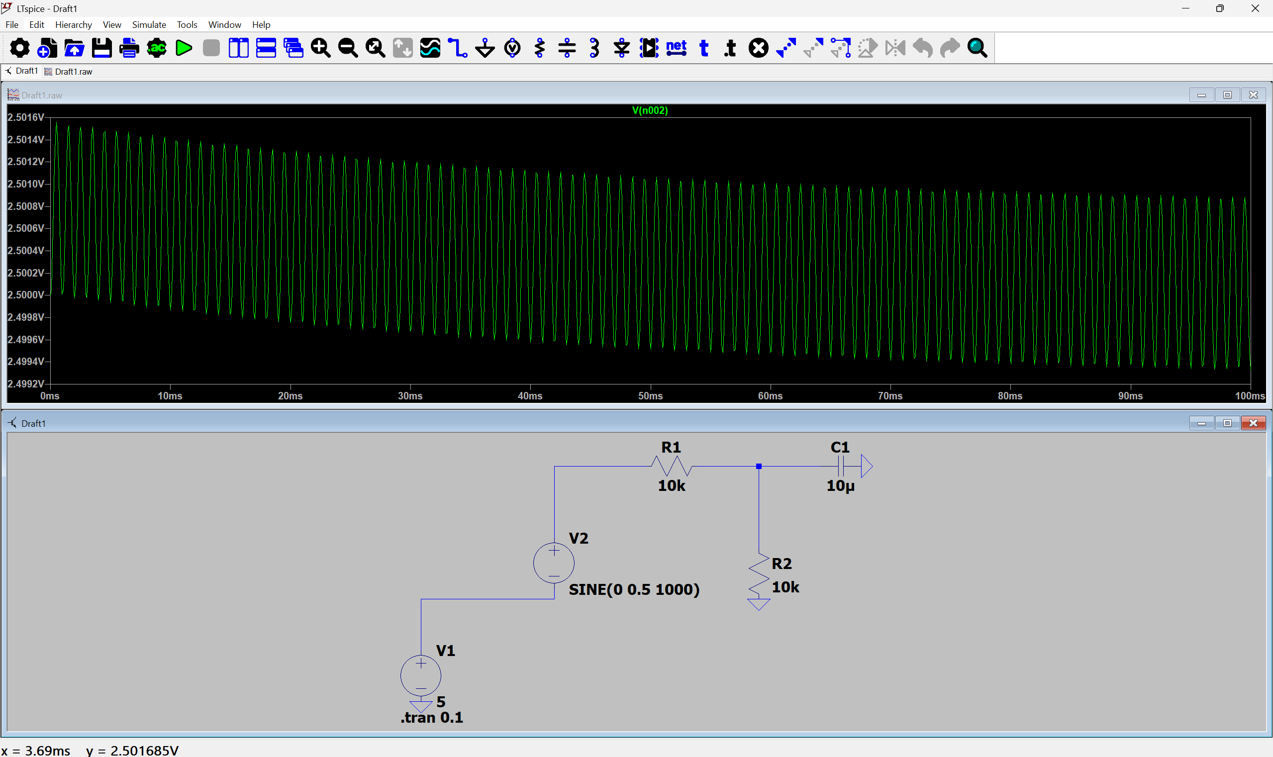
### Circuit Simulation & Validation (LTspice) Before committing any design to PCB, key circuit behaviors were simulated in LTspice to reduce fabrication risk. **Voltage divider model:** The Velostat layer was modeled as a variable resistor in a voltage divider configuration. The simulation confirmed the expected output voltage range across the tine travel distance and identified the sensitivity curve — helping determine the ADC resolution needed.
LTspice simulation — Velostat voltage divider model: schematic and output waveform
LTspice: Velostat modeled as a variable resistor in a voltage divider. Output voltage range validated before PCB commit.
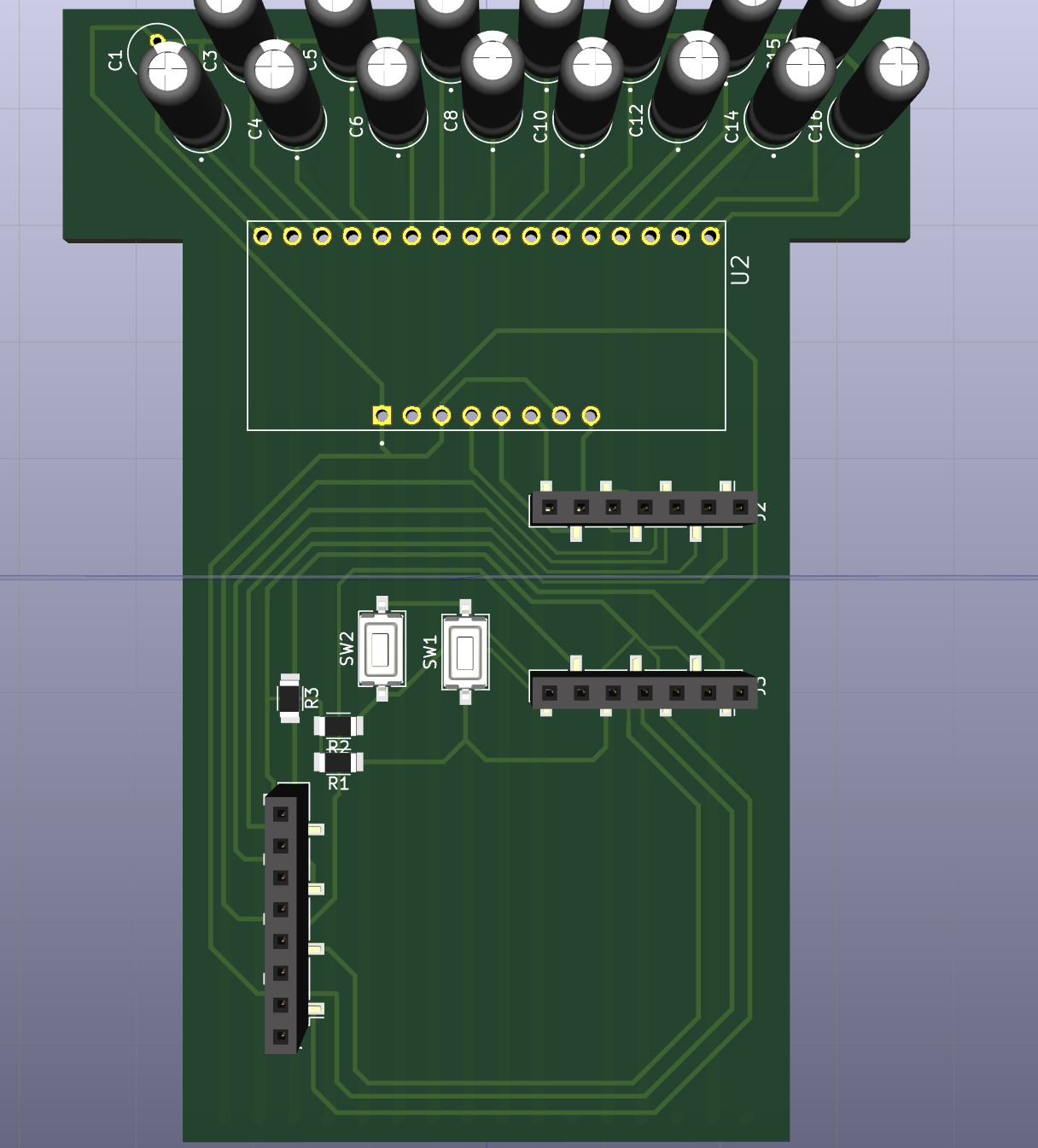
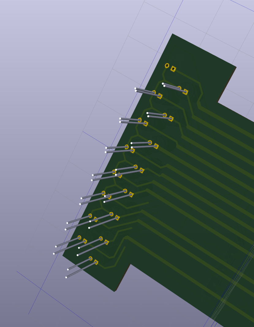
**Capacitor decoupling:** The impact of 0.1µF ceramic decoupling capacitors on power rail noise was simulated. The results confirmed that two capacitors — one at the MCU and one at the multiplexer — were sufficient to suppress the switching transients generated by rapid multiplexer address cycling. **Pull-down resistor behavior — with and without (breadboard validation):** A direct breadboard test was run with a single tine connected straight to the RP2040 ADC pin — no multiplexer at this stage. The setup was minimal: one tine, one wire, one ADC read. The signal on screen was wobbling continuously even when the tine was held still. Adding a single capacitor directly across the RP2040's ADC pin and GND stopped the wobbling immediately — the curve settled and tracked cleanly. Adding a resistor alongside the capacitor, however, locked the signal in place entirely — the ADC reading froze and stopped responding to tine movement. The conclusion was clear: the capacitor alone was the correct intervention for this configuration, acting as a simple RC low-pass filter without pulling the signal to a fixed reference. The resistor was ruled out for the direct ADC input path as a result. ### Microcontroller Selection Two microcontrollers were evaluated in depth to determine the best fit for the project requirements: | Parameter | XIAO ESP32C3 | XIAO RP2040 | | :--- | :--- | :--- | | **Architecture** | Single-core 32-bit RISC-V | Dual-core 32-bit ARM Cortex-M0+ | | **ADC Resolution** | 12-bit (0–4095) | 12-bit (0–4095) | | **Analog Noise** | Higher internal variance | Cleaner, lower baseline | | **Firmware Overhead**| Requires aggressive digital filtering | Light averaging loops sufficient | | **Wi-Fi** | Native, built-in | Not available natively | | **LiPo Charging** | Native battery pads | Requires external TP4056 module | | **Simulation** | Wokwi support | Limited Wokwi support | The final PCB design was engineered to be completely dual-compatible. While the **ESP32C3** pin configuration was initially selected for its native Wi-Fi capabilities and excellent Wokwi simulation support during the prototyping phase, the **RP2040** was favored for the final production unit due to its significantly cleaner analog signal characteristics. Because the PCB footprint accommodates both, the MCU remains a completely seamless, drop-in swap. ### Hardware Implementation & PCB Layout * **MCU Footprints:** The hardware layout relies entirely on the ESP32C3 pin mapping. To mount either microcontroller option onto the board, two **Connector_PinSocket_2.54mm:PinSocket_1x07_P2.54mm_Vertical_SMD_Pin1Left** sockets were utilized. * **Display Interface:** A matching **1x08 pin socket** was implemented to interface directly with the TFT screen. * **Routing Strategy:** To maintain a clean layout and efficiently bridge over intersecting PCB traces without escalating to a more complex multi-layer routing scheme, a **0-ohm ($0\ \Omega$) resistor** was utilized as a hardware jumper. I decided to move with a design to be compatible with both ,and the ESP32C3 pin configuration was selected for its Wi-Fi capability and Wokwi simulation support during prototyping. The RP2040 was reconsidered for the final production unit due to significantly cleaner analog signal characteristics. The PCB footprint accommodates both without hardware changes — the MCU is a drop-in swap. ### PCB Design Iterations
3D pcb preview front face
3d pcb preview front face
3D pcb preview front face
3d pcb preview back face
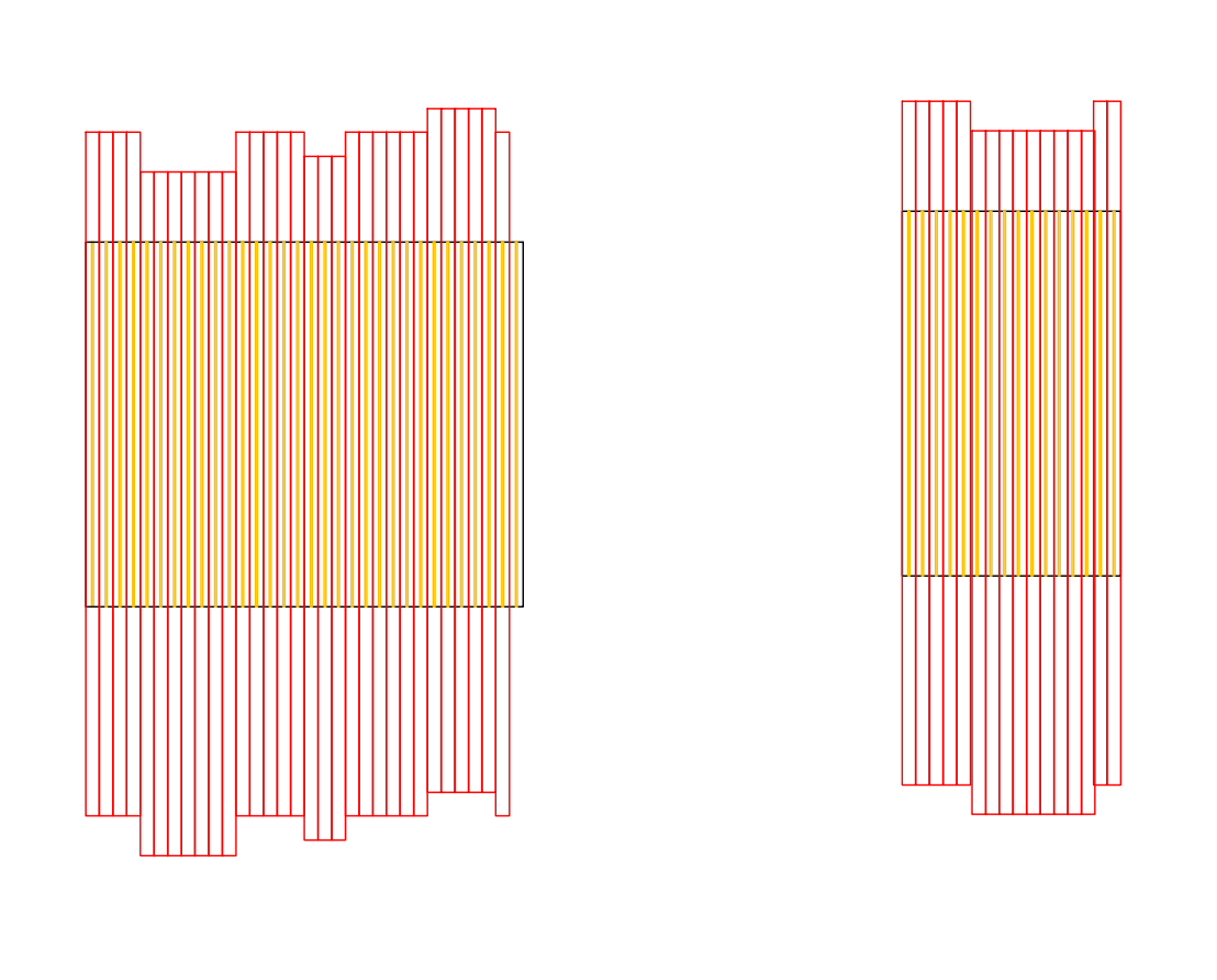
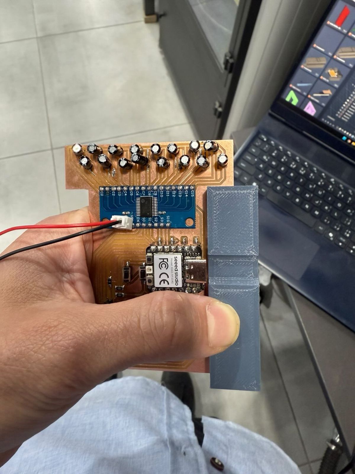
Getting the electronics right for the Digital Contour Gauge (DCG) was a process of trial and error, moving from a messy single-layer layout to a clever workaround using two separate single-sided boards. Here is how the design evolved: * **Schematic Capture:** I started by mapping out the core system in KiCAD. The schematic handles the MCU, the **CD74HC4067** 16-channel analog multiplexer, the SPI TFT display interface, decoupling caps, pull-down resistors, and tactile navigation switches. * **Iteration 1 (The Single-Layer Wall):** My first instinct was to route everything on a single copper layer to keep desktop fabrication quick and painless. It quickly became a nightmare—the sheer volume of trace crossings from the 16-channel multiplexer and display buses made a single layer completely unmanufacturable. * **Iteration 2 (The Routing Fix vs. Fabrication Reality):** Next, I opened it up to a two-layer layout in KiCAD. This easily solved the routing logic, but it introduced a new problem: standard double-sided PCB milling on a desktop machine comes with high registration and flip-alignment risks. If the flip is off by even a fraction of a millimeter, the board is ruined. * **Iteration 3 (The Dual-Board Workaround):** To completely bypass the alignment risk while keeping fabrication straightforward, I came up with a clean manufacturing workaround right from the single KiCAD project file: * **Front Layer Export:** I isolated the top layer (MCU dock, multiplexer logic, I2C pull-ups, decoupling caps, and switches) and exported it to mill as its own standalone, single-sided board. * **Back Layer Export (Mirrored):** I isolated the bottom layer—which contains the 16 parallel vertical traces for the tine array contacts—mirrored it during export, and produced it as a completely separate single-sided board. * **Repurposed Vias:** By sandwiching these two physical boards back-to-back, I was able to use the through-hole component pins as natural structural vias, bridging the two boards mechanically and electrically without needing to drill independent via holes. ### Electronics Proof of Concept — Breadboard Iterations *(Starting from Week 9/10 — full chronological account)* **Stage 1 — Isolated OLED Test (Week 10):** Before any integration, the SSD1306 OLED was tested in isolation on an Arduino UNO breadboard to confirm the screen itself was functional — following a troubleshooting dead end on the custom PCB. The issue was identified: the physical module had VCC and GND swapped relative to the KiCAD footprint. Corrected and confirmed working.

No input detected test, then a flybird inspired test run !

**Stage 2 — Single and Two Potentiometer → Curve Plotting (Week 11):** A single 50kΩ potentiometer was connected to the RP2040 through the multiplexer (channel J1, all address pins LOW). The raw ADC value was smoothed using an EMA (Exponential Moving Average) filter and mapped via `map()` to the OLED's 64-pixel height. The output was a real-time scrolling waveform — the first visual proof that the sensor → display pipeline worked. This also became the "Playstation on a Budget" Flappy Bird-style game demo.

Digital Contour Gauge Mockup - Breadboard

This video demonstrates a part of my final project iterations to explore the potential setup for my final project.

This video demonstrates the code I uploaded to my new PCB working. On the left, it shows how the PCB communicates via UART and the Python code, where it shows a message confirming data sent from the obstacle sensor. On the right, it shows the obstacle sensor on the serial monitor to confirm the sensor is in fact working and to verify.

This video shows the computer side and the Python program running after receiving data from the obstacle sensor and PCB, where we start by running obstacle.py and it starts listening for information from the PCB connected to the PC port. The video later on shows the data being received as expected.

Digital Contour Gauge Mockup - Computer Side

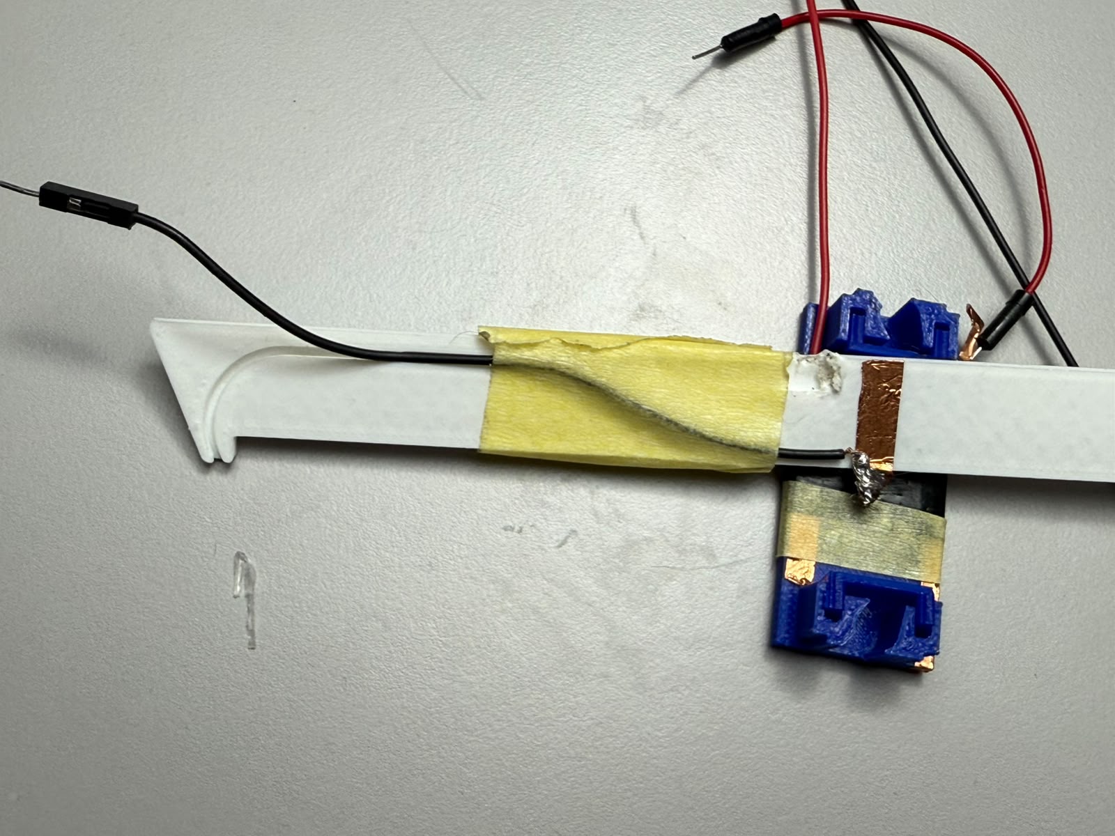
**Stage 4 — Replacing One Potentiometer with a Tine Mockup (Week 11):** One potentiometer was removed and replaced with the first physical tine mockup: a 3D-printed tine with a copper tape contact, sliding over a Velostat strip with copper tape busbars. This was the critical transition from simulated input to real sensor input.

# Firmware and Software Development The firmware ended up becoming the biggest part of this project. My original goal was simply to build a digital contour gauge that could measure an object's profile using sixteen sliding sensing tines and display the shape on a screen. As development progressed, the project grew into much more than that. Besides reading the sensors, the firmware also had to draw a live contour, store scan data, communicate with a computer, generate CAD models, and provide a simple interface that anyone could use. I developed the software one feature at a time. Every time I solved one problem, another one appeared. Instead of trying to write everything perfectly from the beginning, I kept improving the code as new challenges came up. Looking back, most of the project was spent debugging and refining rather than writing new features. ## Reading the 16 Sensor Channels The first challenge was reading all sixteen sensing tines using only one analogue input on the RP2040. To achieve this, I used a CD74HC4067 sixteen-channel analogue multiplexer. Four digital output pins act as address lines, allowing the microcontroller to switch between each channel before taking an analogue reading. ```cpp int readMux(int channel) { digitalWrite(S0, bitRead(channel,0)); digitalWrite(S1, bitRead(channel,1)); digitalWrite(S2, bitRead(channel,2)); digitalWrite(S3, bitRead(channel,3)); delayMicroseconds(30); return analogRead(SIG); } ``` This function became the heart of the entire project because every measurement passed through it. At first I noticed the readings were unstable and randomly jumping between values. After testing different possibilities, I realised the multiplexer needed a very short settling time after changing channels. Adding a 30 microsecond delay before taking the analogue reading made the measurements much more stable. Once I could reliably read all sixteen channels, I finally had the data needed to build the rest of the system. --- ## Displaying a Live Contour After obtaining stable sensor values, the next goal was displaying the object's profile on the TFT screen. Instead of showing sixteen separate numbers, I wanted the gauge to look like a real contour scanner. Each sensor value was calibrated, converted into a screen coordinate, and connected with neighbouring points to create one continuous line. ```cpp mappedY = 65 - (normalizedScalar * (65 - 22)); ``` Watching the contour move in real time as the tines followed an object's surface was one of the most rewarding moments during development. It was the first time the hardware and software worked together exactly as I had imagined. To reduce flickering, I avoided clearing the whole display every frame. Instead, the firmware erased only the previous line before drawing the updated contour. This made the display much smoother while reducing unnecessary SPI communication. --- ## Solving Hardware Problems in Software Not every problem came from the code. During testing I discovered that two channels occasionally behaved unpredictably. My first thought was that I had introduced a bug into the firmware, so I spent a long time checking the code. Eventually I discovered that the issue was caused by my custom PCB rather than the software. A routing problem allowed signals to bleed into neighbouring lines. Rather than redesigning the PCB immediately, I temporarily isolated the affected pins in software so I could continue developing the rest of the project. ```cpp pinMode(7, INPUT); pinMode(8, INPUT); ``` This solution wasn't intended to replace proper hardware design, but it allowed me to continue testing while preventing the faulty signals from affecting the remaining channels. --- ## Building a Simple User Interface I wanted the contour gauge to be easy to use without adding lots of buttons. Instead, I created a menu system that uses only one push button. A short press moves through the available options, a double press quickly returns to live scanning, and holding the button enters the selected menu option. Although this sounded simple, getting the timing right took several attempts. The firmware had to distinguish between short presses, double clicks and long presses without accidentally triggering the wrong action. I also added an on-screen progress bar so the user could clearly see when a long press was being detected. This made the device much easier to operate while keeping the hardware simple. The user interface delivers a real-time visualization station styled after retro terminal systems. It parses and loops through incoming master JSON data matrices using a background polling thread. Key Interface Features: - Multi-Node Vector Canvas Projections: The interface dynamically tracks the 16-channel datasets, executing coordinate translation matrix calculations to reconstruct high-accuracy line profiles inside modern web spaces. - Multi-Slice Opacity Viewports: Operators can toggle between an isolated slice layer view or a global historical projection view (which stacks all stored slices simultaneously with graduated opacity treatments to highlight dimensional deformation trendlines). - Client-Side DXF Compiler Assembly: Features an internal client-side vector construction layer. This allows field operators to build and export standard 3D CAD vectors directly out of the browser panel, eliminating the need for separate workspace compilation tools. --- ## Sending Scan Data to the Computer Once live scanning was working, I wanted a way to save profiles and generate CAD models automatically. Rather than sending complicated binary packets, I decided to transmit plain text over UART because it was easy to debug using the serial monitor. ```text START_DATA SCAN:0,... SCAN:1,... END_DATA ``` Using simple start and end markers allowed the computer to recognise when a complete scan session had arrived. Every scan contains the position of all sixteen sensing tines, allowing the entire profile to be reconstructed later. Keeping the communication protocol simple also made debugging much easier whenever something went wrong. --- ## Python Bridge Receiving the data on the computer became the next challenge. I wrote a Python application that constantly listens to the serial port waiting for incoming scan data. ```python line = ser.readline().decode('utf-8').strip() if line == "START_DATA": ``` Once a complete scan is received, the program automatically processes the measurements, generates a DXF model, creates JSON files for the web interface, and stores every scan in a history folder. ```python doc = ezdxf.new("R2010") ``` One feature I added later was duplicate detection. During testing I sometimes accidentally captured identical profiles more than once. The program compares each incoming scan with previous scans and ignores duplicates, preventing unnecessary files from being generated. Automating this process meant I could scan an object and immediately have a CAD model ready without manually copying any data. --- ## Interactive Web Viewer Although the Python program successfully generated DXF files, repeatedly opening AutoCAD while testing became slow and inconvenient. I wanted a faster way to view scans, so I built a browser interface that automatically displays the latest results. The interface continuously checks for new JSON data generated by the Python bridge. ```javascript setInterval(pollLive, 1500); ``` Each scan is drawn using the HTML canvas by connecting all sixteen measured points together. ```javascript ctx.lineTo(x, y); ``` The interface also keeps a history of previous scans, allows individual slices to be viewed, and can export the displayed profile as a DXF file directly from the browser. This made testing much faster because I could immediately see whether a scan looked correct before opening it in CAD software. --- Python Pipeline Core Processing Modules:
LibraryRole
serialHooks the active hardware port connection, running structural timeout limits to catch incoming packets.
ezdxfAssembles the 16 separate horizontal coordinates per row into high-precision, continuous polyline entities inside full 3D CAD vectors.
jsonSerializes multi-point slice packages into persistent log file registries.
osValidates file structural access paths and handles multi-layer atomic file buffering.
timeAppends UNIX file timestamps for long-term profiling histories.
Key Engineering Solutions Realized: - Automated Z-Depth Slicing (3D Extrusion Modeling): For every discrete sequential SCAN frame captured, the Python bridge increments the depth calculation index (Z = scan_index × TINE_PITCH). This naturally maps the 16 independent 2D point arrays into a structured, stacked 3D contour shell directly inside CAD workspaces. - Data Deduplication Filtering: Compares incoming datasets against an active uniqueness tracking set (seen_profiles). If duplicate profiles are captured, the pipeline drops them instantly to ensure CAD models remain clean. - Safe State Write Guards: Implements file-locking buffering sequences (atomic_write) when generating updates to prevent desktop polling crashes during browser reads.

## Mechanical Design & Manufacturing ### CAD Workflow (Fusion 360) The mechanical design followed a design-thinking approach: define → ideate → prototype → iterate. - **Dimensional constraint sheet (AutoCAD first):** Before touching Fusion, a 2D dimensional constraint sheet was produced in AutoCAD. This defined the critical envelope dimensions: tine pitch (3mm), tine travel (50mm), PCB dimensions (from KiCAD), enclosure outer envelope, and the clearance gaps for wiring paths. - **Fusion 360 parametric modeling:** The enclosure and tine assemblies were built as parametric models, meaning changes to a master parameter automatically propagated through the full assembly. - **CAD → KiCAD → CAD loop:** The PCB dimensions in KiCAD were set first, exported as a DXF board outline, and imported into Fusion as a reference sketch for the enclosure floor. **Design checklist completed:** - [x] 2D Dimensional Constraint Sheet (AutoCAD) - [x] Full KiCAD design file and component definition - [x] Full 3D Fusion design file and visualization
AutoCAD 2D dimensional constraint sheet — all key envelope dimensions and clearance specs
AutoCAD dimensional constraint sheet — all key envelope dimensions defined before any 3D modeling began.
Interactive 3D model: DCG_V3 assembly design exploration.
DCG V3 — final parametric assembly. All dimensions driven from the KiCAD PCB outline imported as a reference sketch.
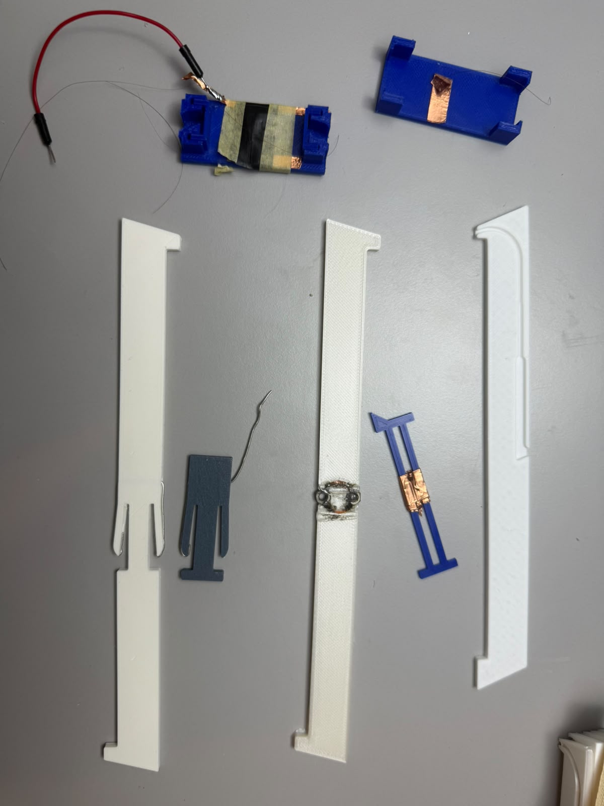
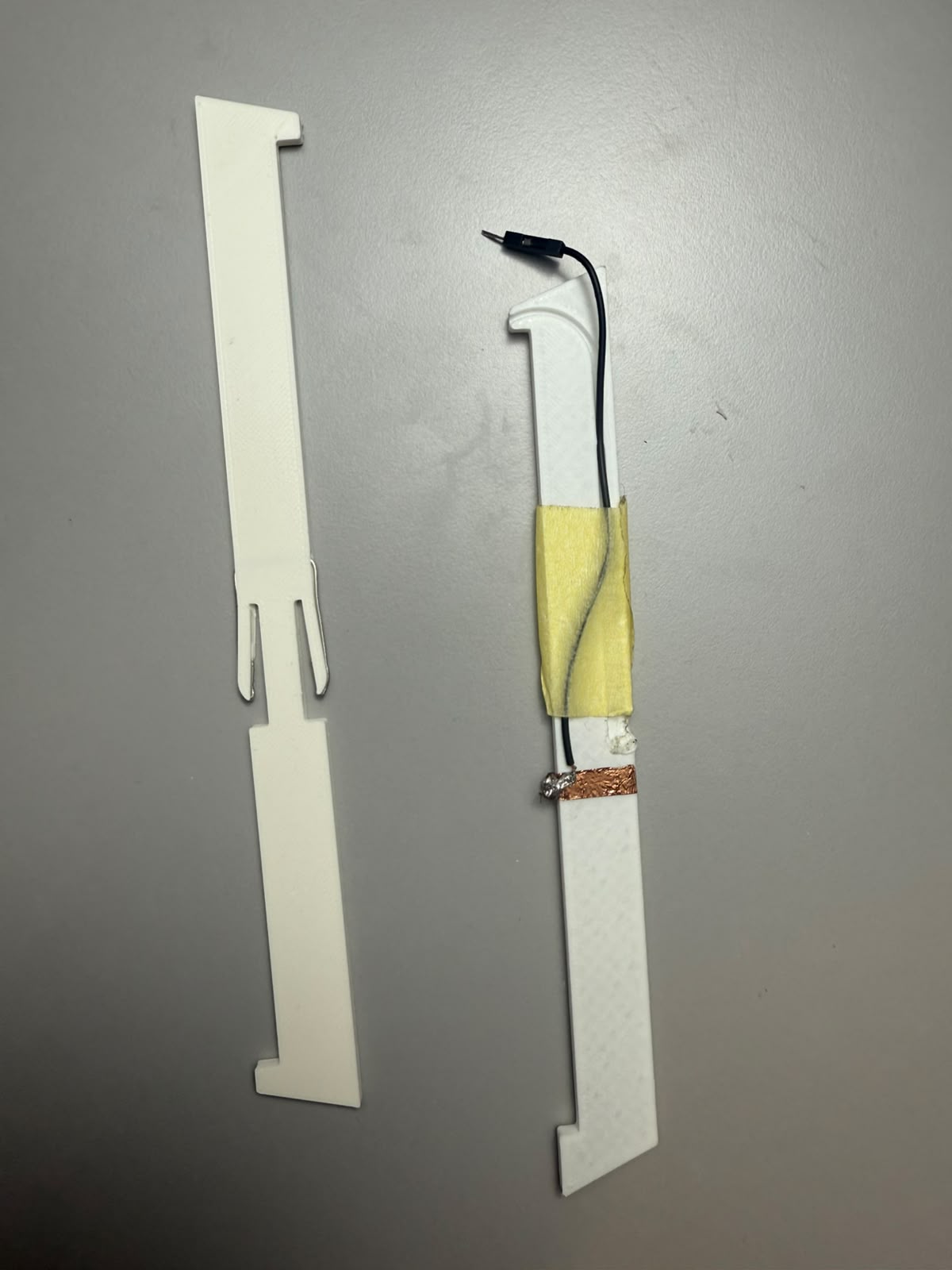
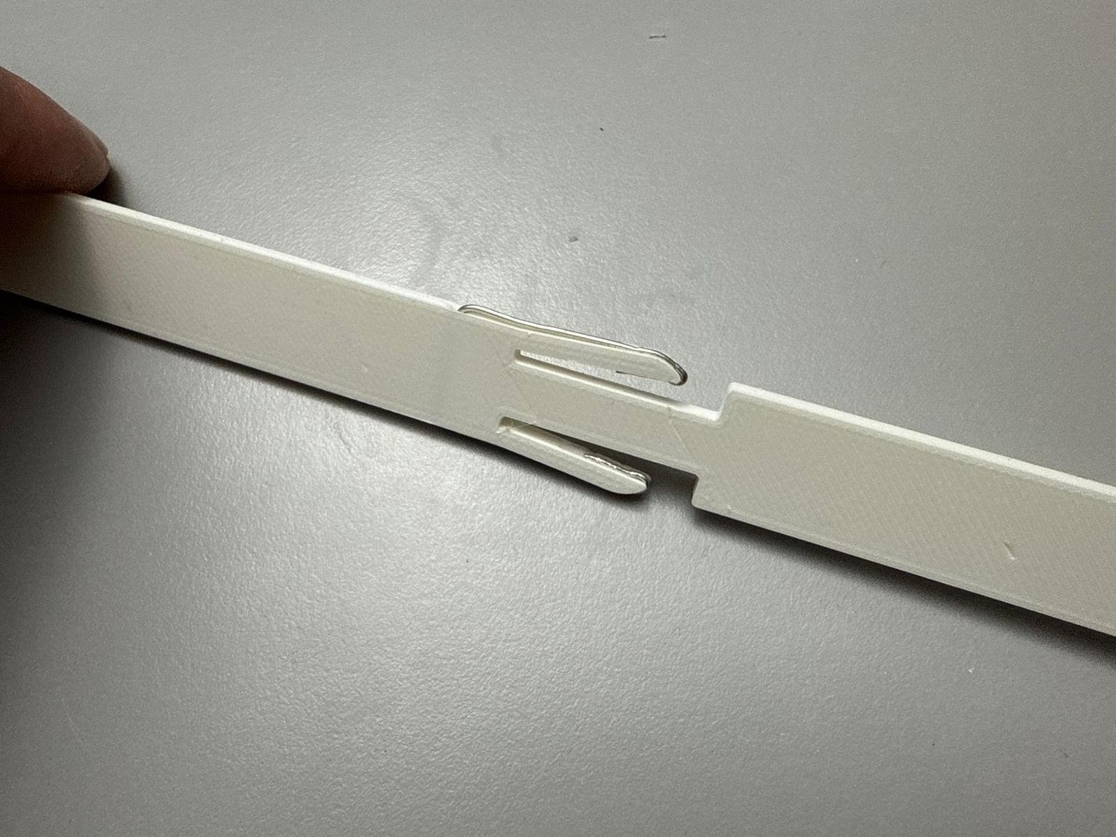
### Tine Design & Evolution The tine is the central mechanical element — it must be narrow, spring-loaded, structurally rigid, and electrically conductive at its tip.
Tine Evolution Progress
### Enclosure & Chassis The enclosure shifted with rapid prototyping different 3D models and prints. I started off by modeling my PCB inside of Fusion; I chose to do that manually as importing from KiCAD would not have given me the accuracy I need for the expected actual outcome. That is because I am modeling the electronics on KiCAD yet producing two single-layer PCBs, with specific extrusion depths for the milled traces which are important to consider since I am relying on pressure and spring loads, so tolerances are at a minimum. I then began iterating enclosures and below is the evolution sequence of the design from my 32 preliminary model, narrowed to a space of 16 tines. #### Iteration 1: #### Iteration 2:
3d printing the first enclosure version
testing the fit in respect to the pcb
testing the fit in respect to the pcb, tft screen clashed with the right enclosure piece
as built modifications to fit for the tft screen overlap with the enclosure in assembly
as built modifications to the right enclosure piece
testing the fit in respect to the pcb
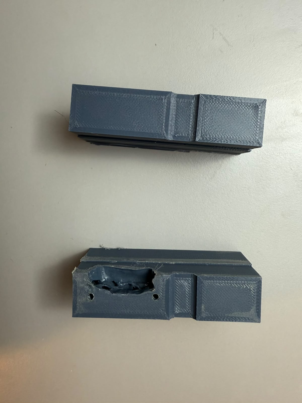
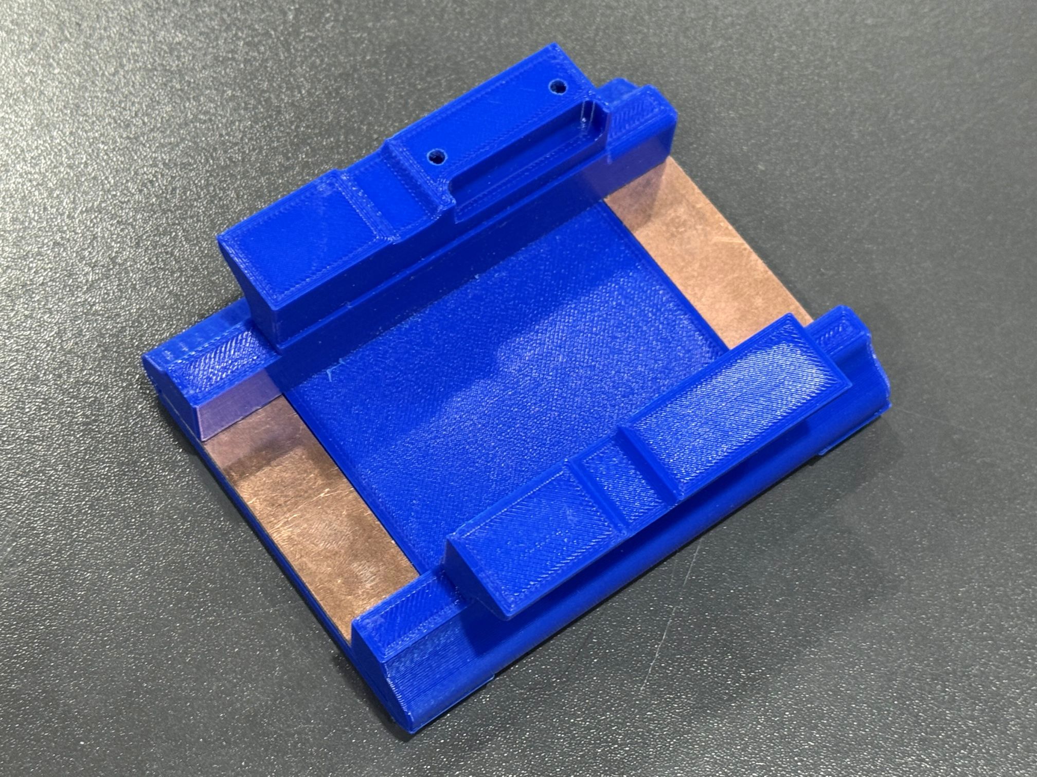
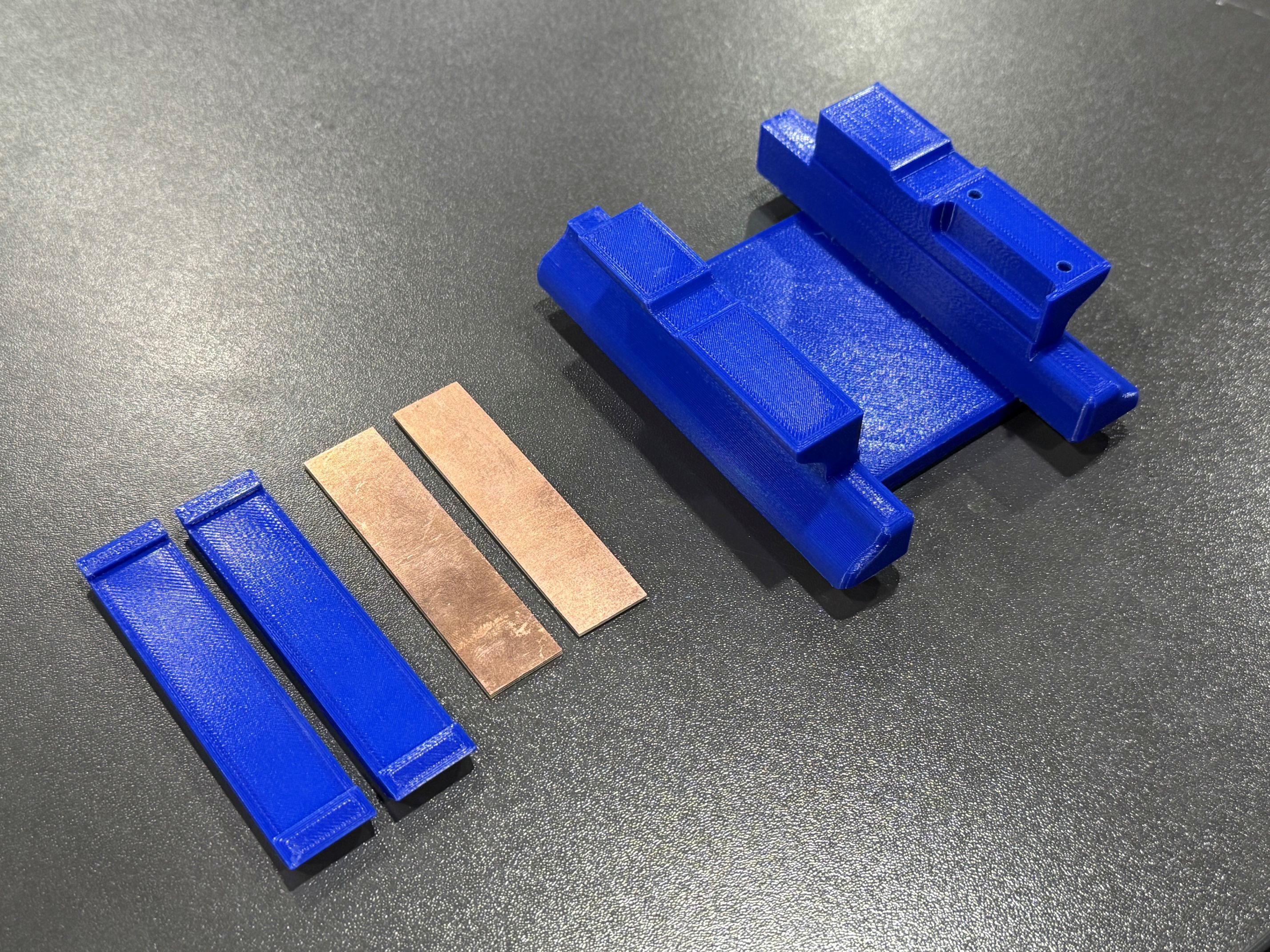
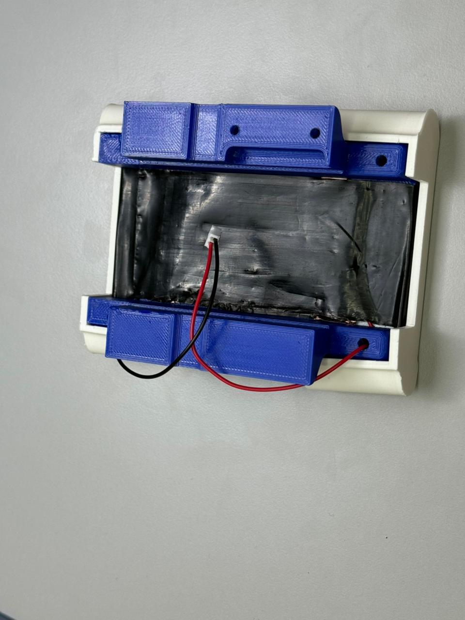
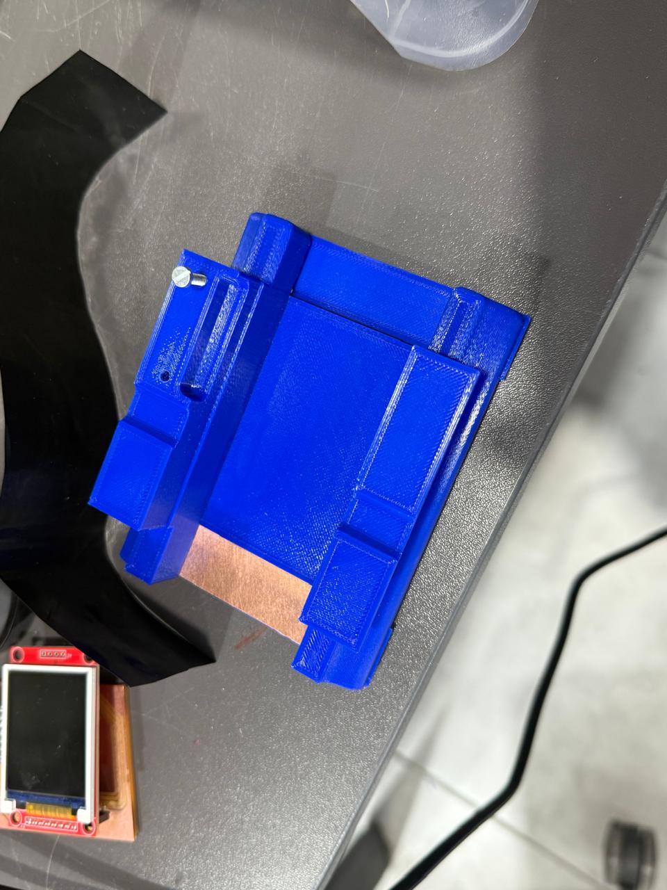
### Final Enclosure Design The final version included two clamp-on pieces which serve to clamp on the velostat and assemble the enclosure at the same time. The full enclosure transitioned to a single continuous piece and was dimensioned and extruded to fit everything in place at once, leaving space for the common busbar rails on the top and bottom. Note: I did all the drilling/holes manually to ensure an exact as-built alignment of the components. The two holes in the final enclosure at the ends served as wire entry points to the common bus/gnd rails without interfering with the tine pathway. I also used a JST connector soldered to the PCB as shown to ensure quick assembly and disassembly.
Final Enclosure Assembly- Holes manually drilled
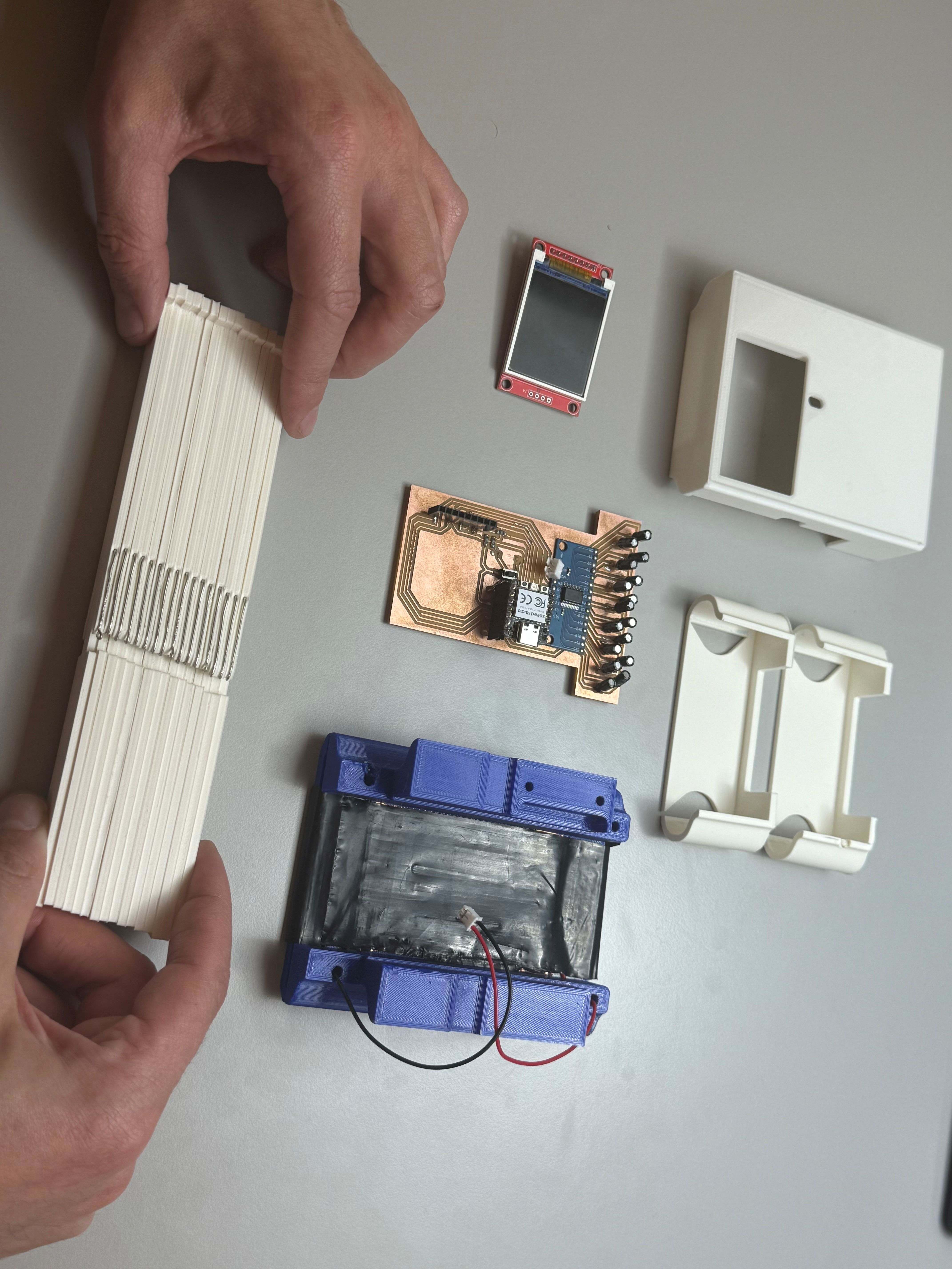
Final Enclosure exploded
Final enclosure exploded/parts
Final Enclosure exploded
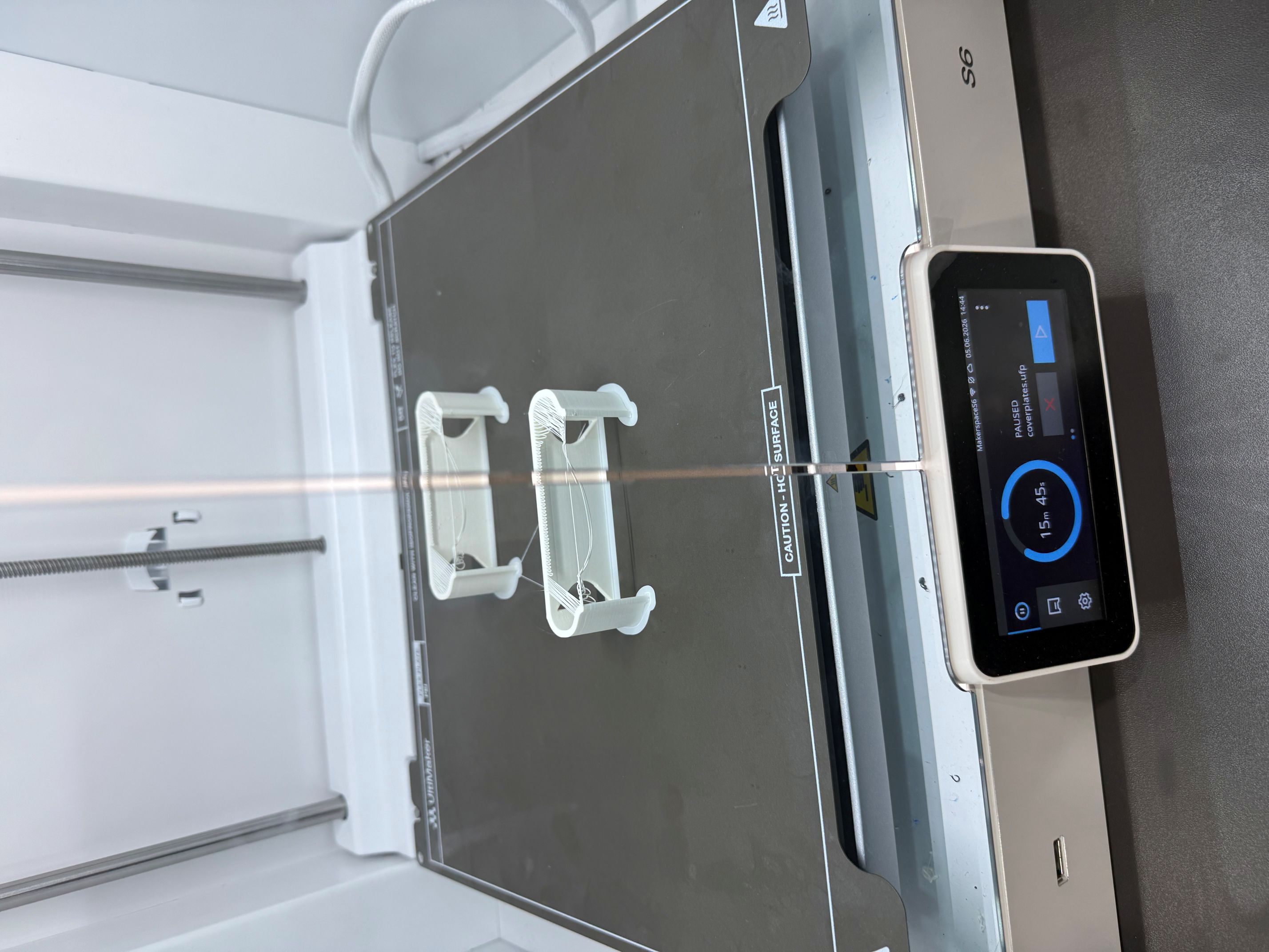
3D printing the top and bottom clamps/ failure here because i forgot to place the model properly in the slicer/top layer overhang failure
Final Enclosure assembly with clamps
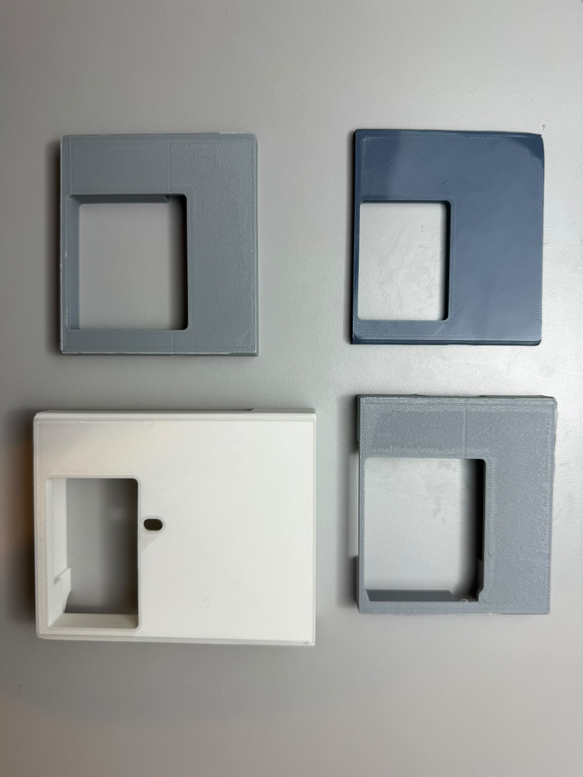
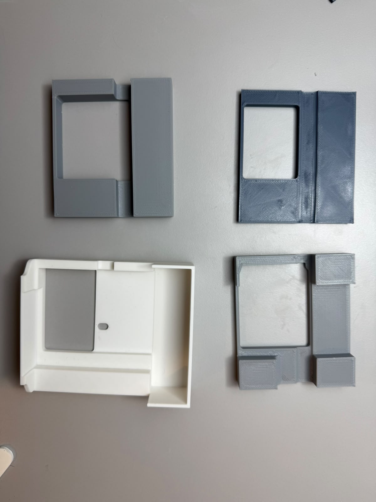
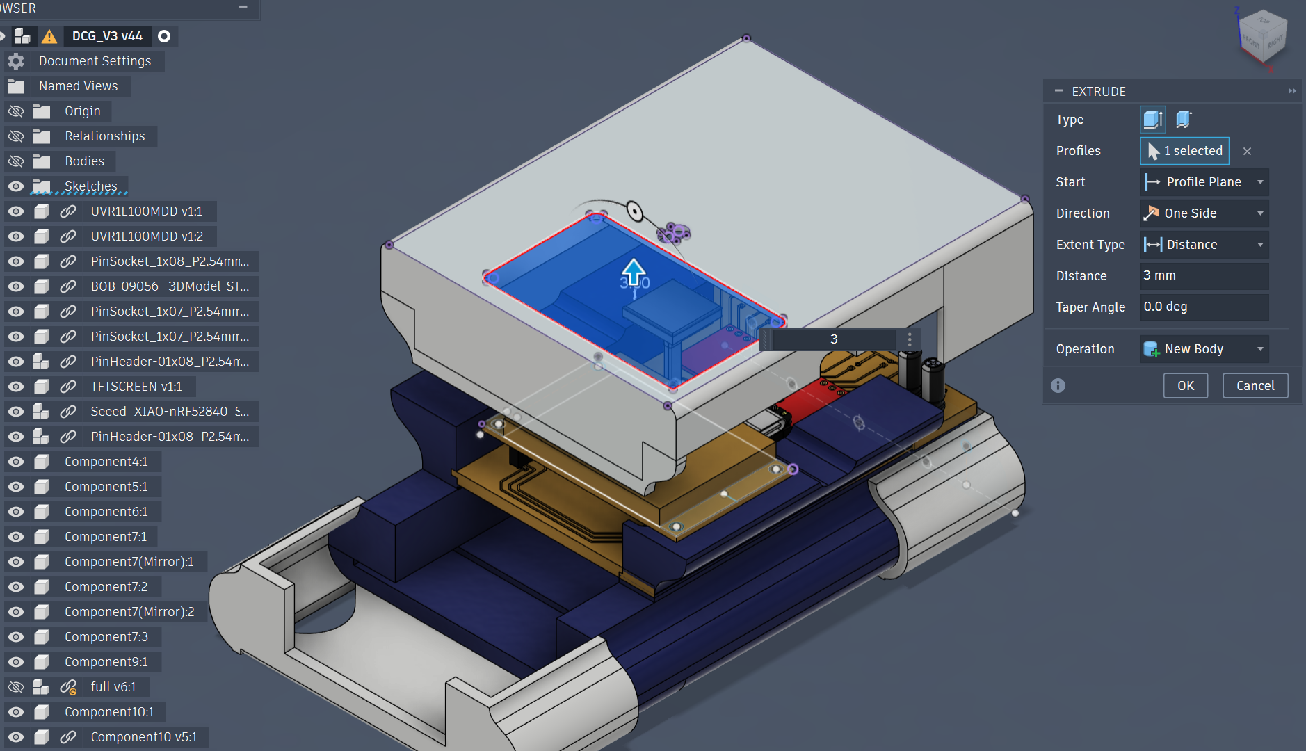
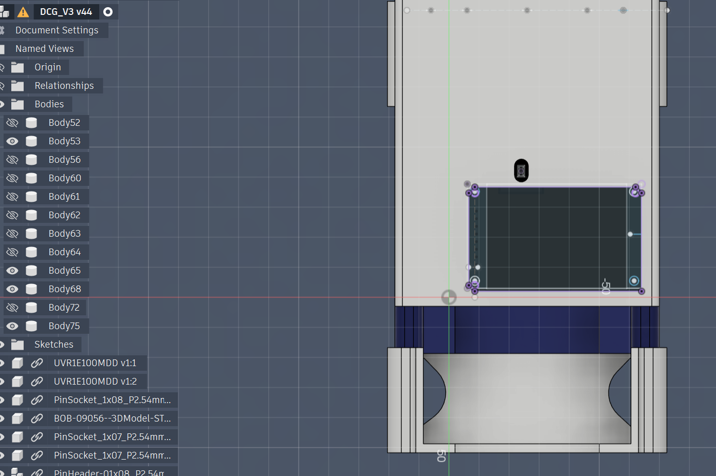
### Top Cover plate The top cover plate was a pickle, as I tried 4 versions between aligning the cover on top of the PCB with all the electronic component offsets.
From left to right, I started with a thin extrusion,cleared path for type c plug, realized there is more and more to clear out to make everything fit
From left to right, I started with a thin extrusion, cleared path for type-c plug...
From left to right, I started with a thin extrusion,cleared path for type c plug, realized there is more and more to clear out to make everything fit
Further housing modifications to clear out and make everything fit perfectly.
### Final Assembly Model

DCG_V3 by m.azizi2793 on Sketchfab

### Sub-Assembly Breakdown
Sub-AssemblyDescription
SA1 — Back Plate and ClampsHouses the two common copper busbars (Gnd and PWR) and encloses to the chassis
SA2 — Tine Array16 spring-loaded sliding tines with embedded steel wire wiper contacts, packed into precision guide tracks
SA4 — Electronic Module CasingProtective top cover preventing particulate contamination of the sensor electronics also pushes the PCB to the spring loaded tines
SA5 — Dual-PCB SubstrateTwo milled single-sided FR1 copper boards designed to face each other and close the sensor contact loop
Sub-assembly SA1 — back plate engine, alone before full assembly
Sub-assembly SA1 — back plate engine layout prior to final assembly.
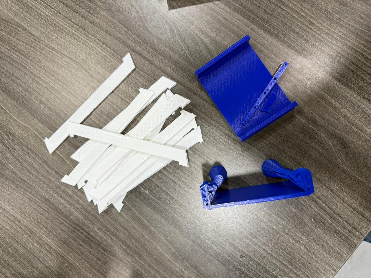
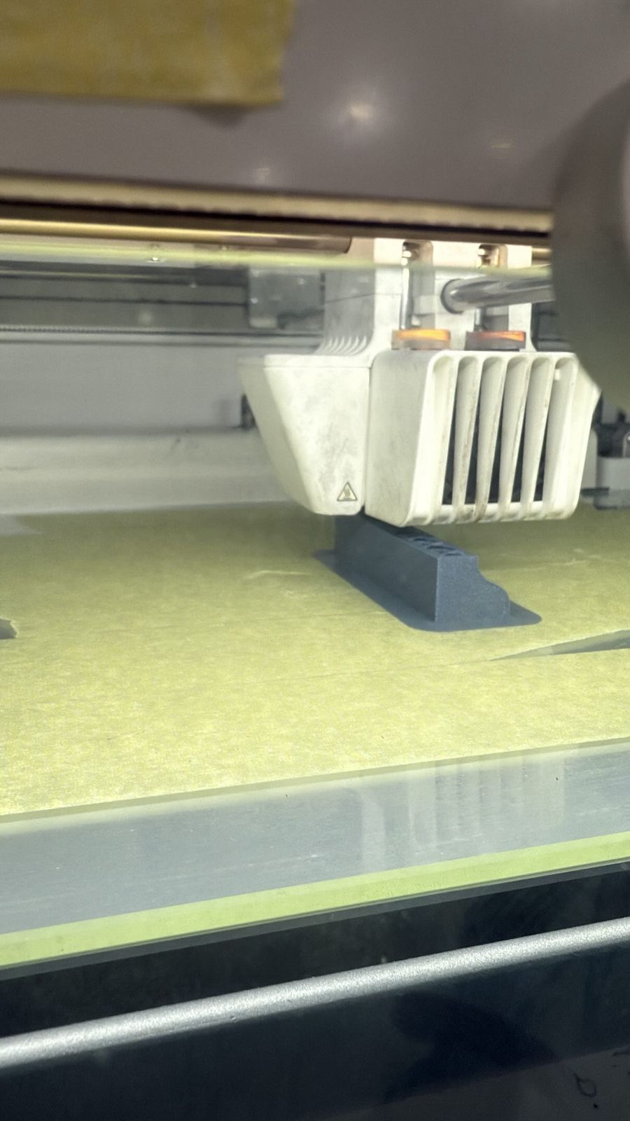
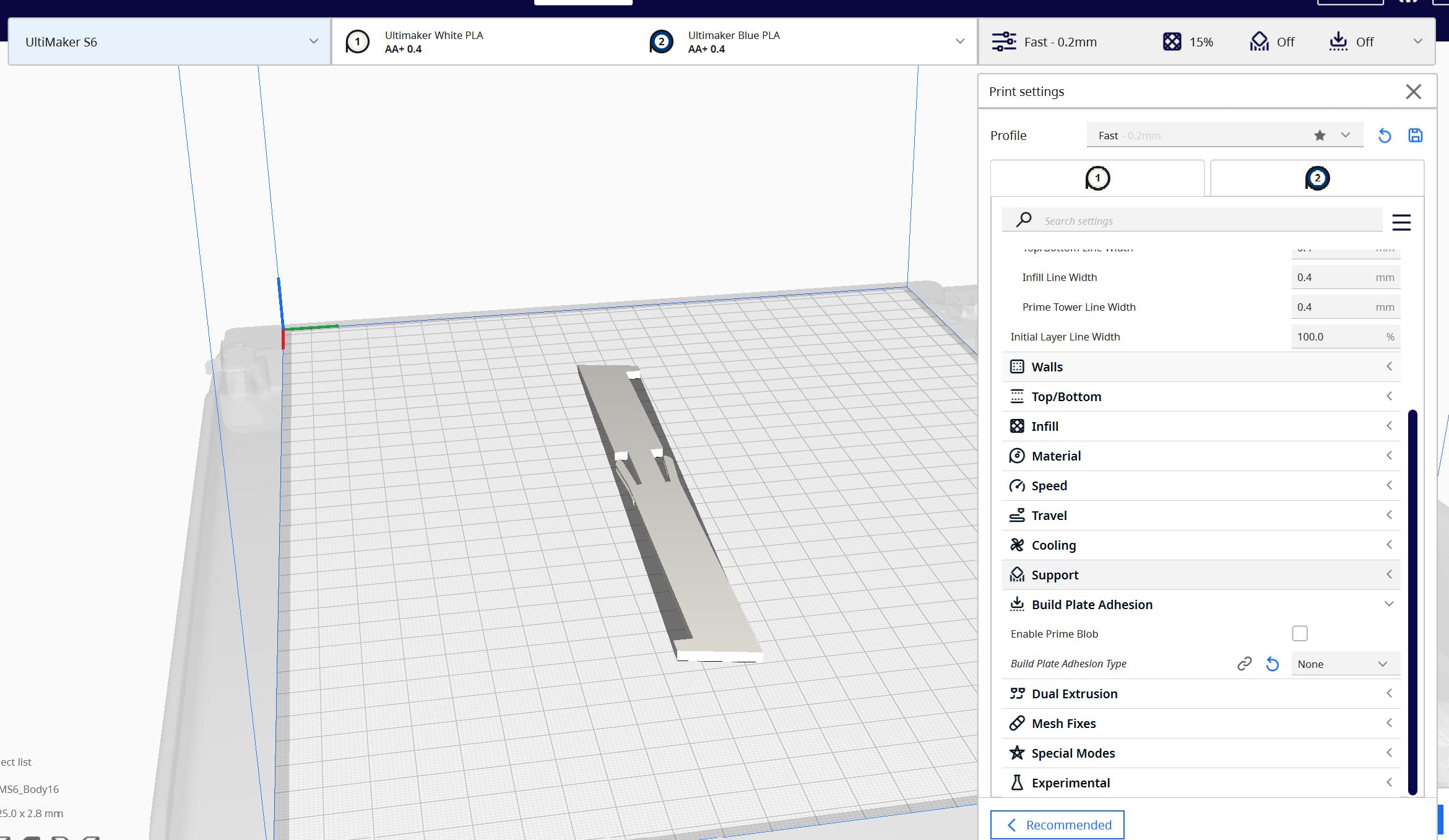
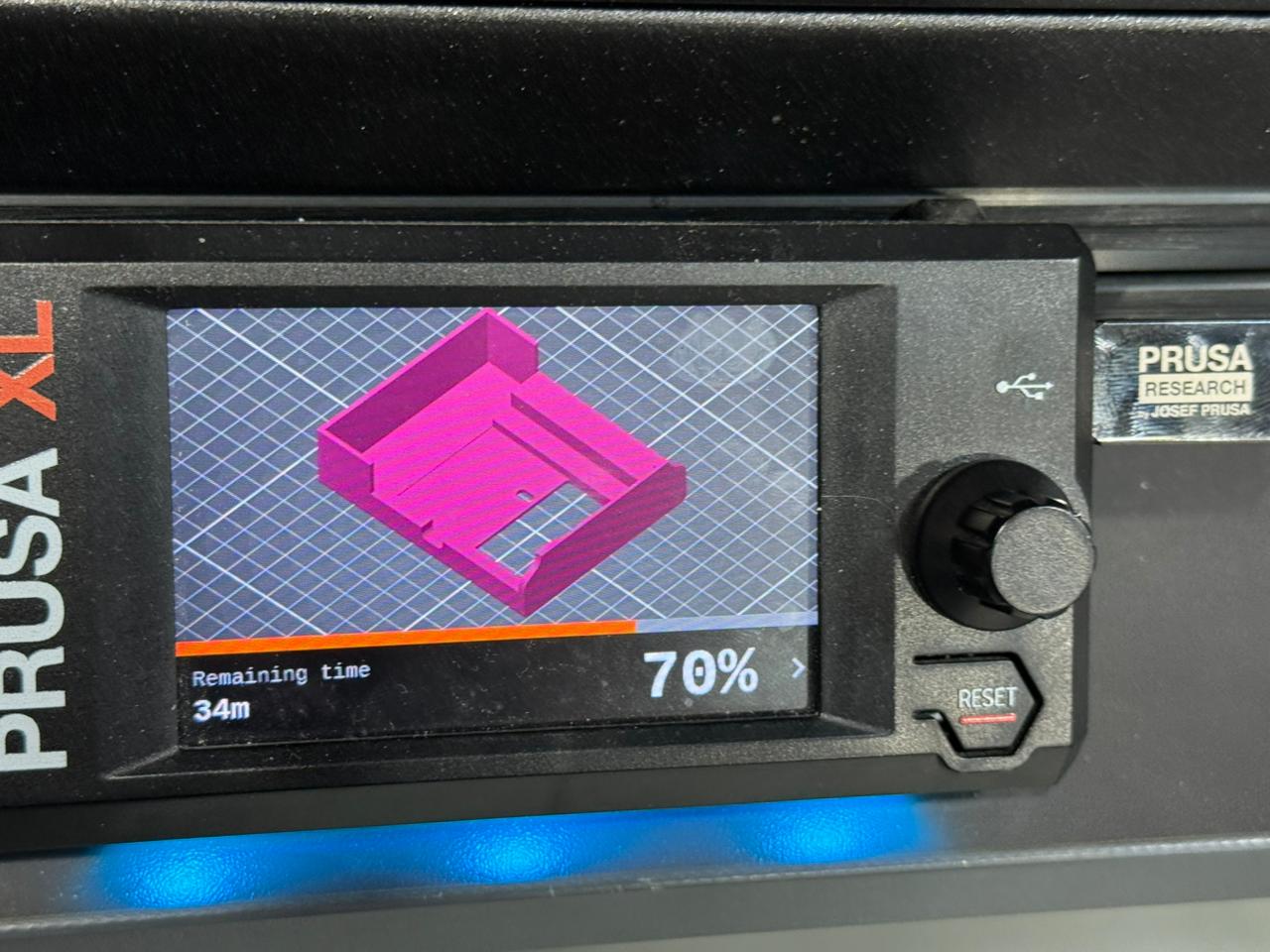
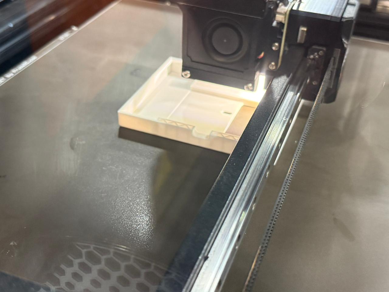
### FDM Manufacturing Process - **Ultimaker S5 / S6:** Used for the main enclosure chassis, Clamps, and Tines. - **Prusa XL:** Used for Front Cover. - **Materials:** White PLA (chassis), Blue PLA (tines). - **Slicer (Cura):** Layer height 0.2mm, nozzle 0.4mm, overhangs designed under 45° to minimize supports.
Tine Print Slicer settings in Cura
Tine Print Slicer settings in Cura, adhesive set to none.
Front Cover Print - Prusa XL
Sub-assembly Front Cover Print - Prusa XL
Front Cover Print - Prusa XL structural detail.
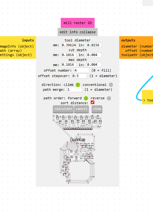
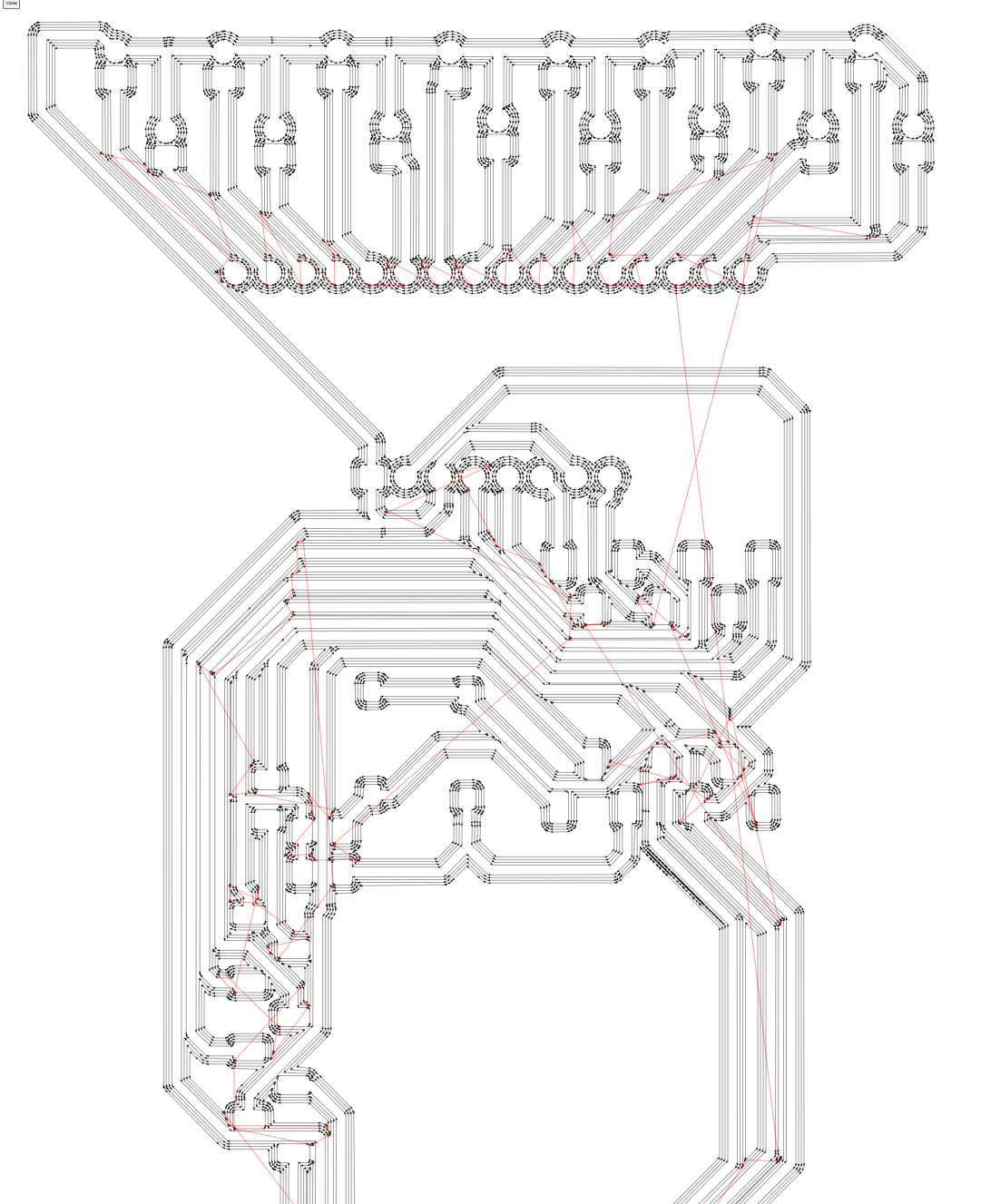
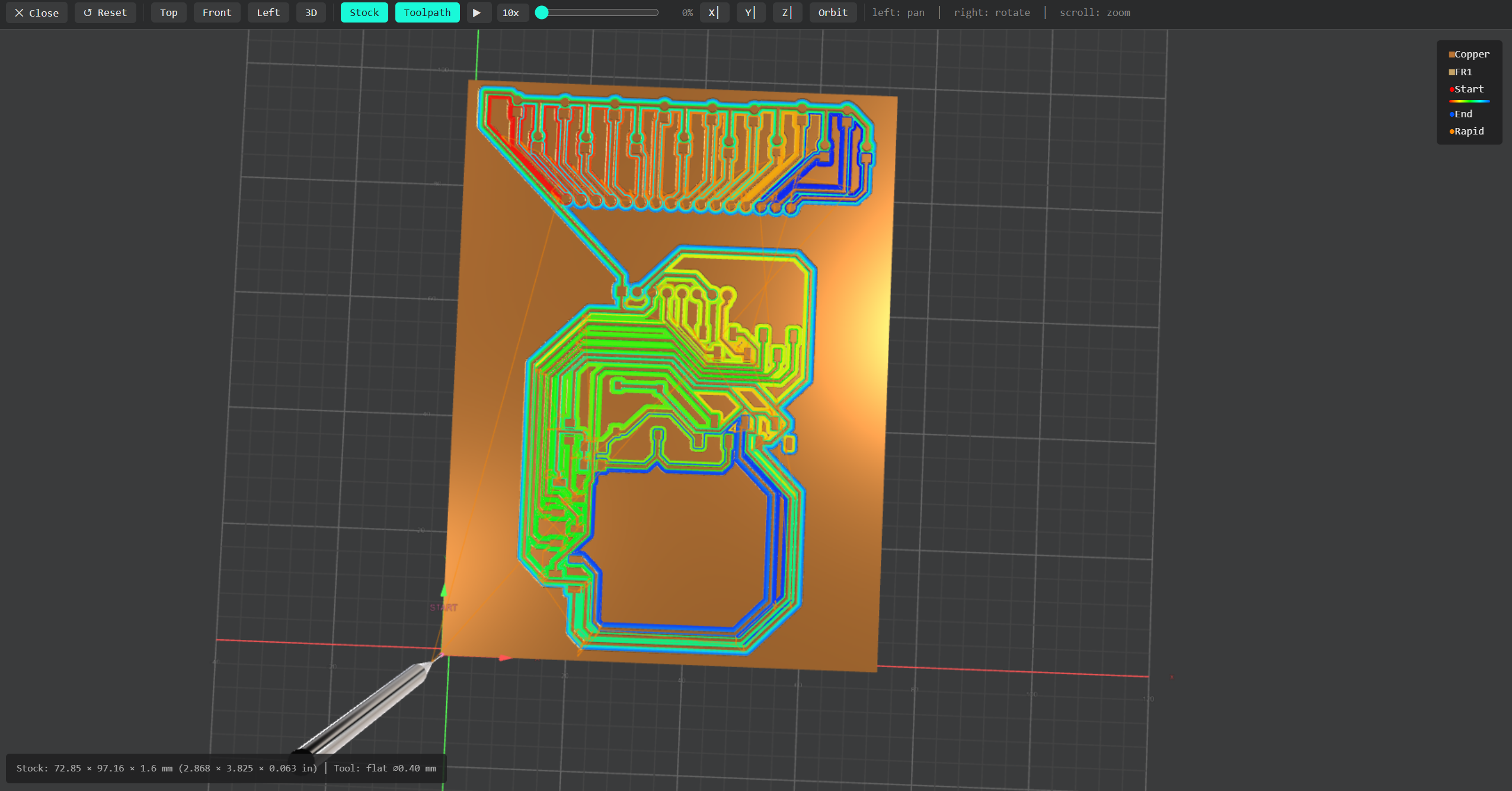
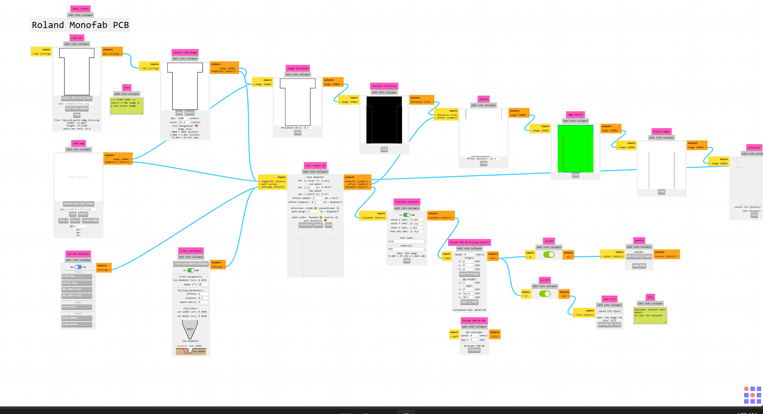
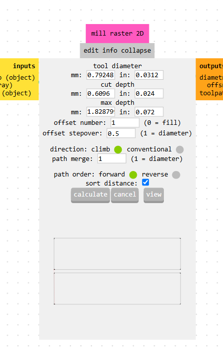
### PCB Milling Workflow (Roland SRM-20 + Mods CE) 1. **Gerber export from KiCAD:** Front copper, back copper, edge cuts, and drill files. 2. **Mods CE toolpath generation:** V-bit isolation milling (0.1mm depth), end mill for board outline cutout. 3. **Roland SRM-20 operation:** FR1 taped down, XY/Z zeroed, front copper milled, board flipped on alignment pins for back copper, cutout last. 4. **Post-mill inspection:** Multimeter point-to-point continuity check on all traces before soldering.
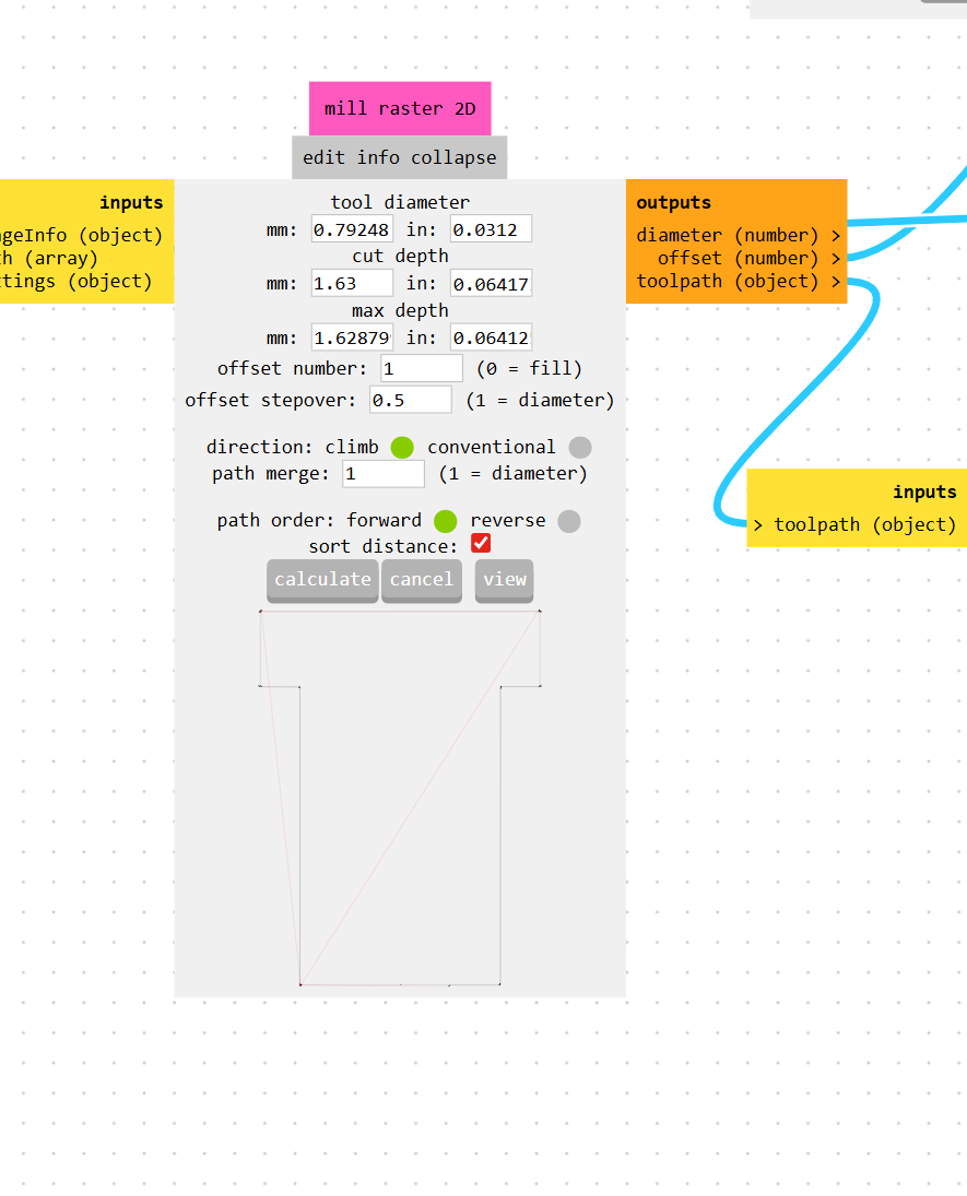
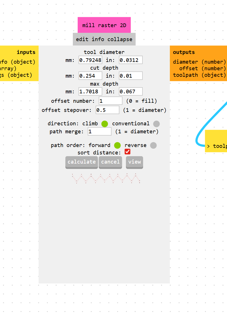
Mods CE settings for front copper layer milling raster 2D
1. Traces Setup: Setting up the 2D mill raster for the front copper logic paths using a 0.396mm (1/64") tool with 4 isolation offsets.
Detailed view of the calculated vector trace isolation paths
2. Tool Path Preview: A close look at the vector toolpath calculation.
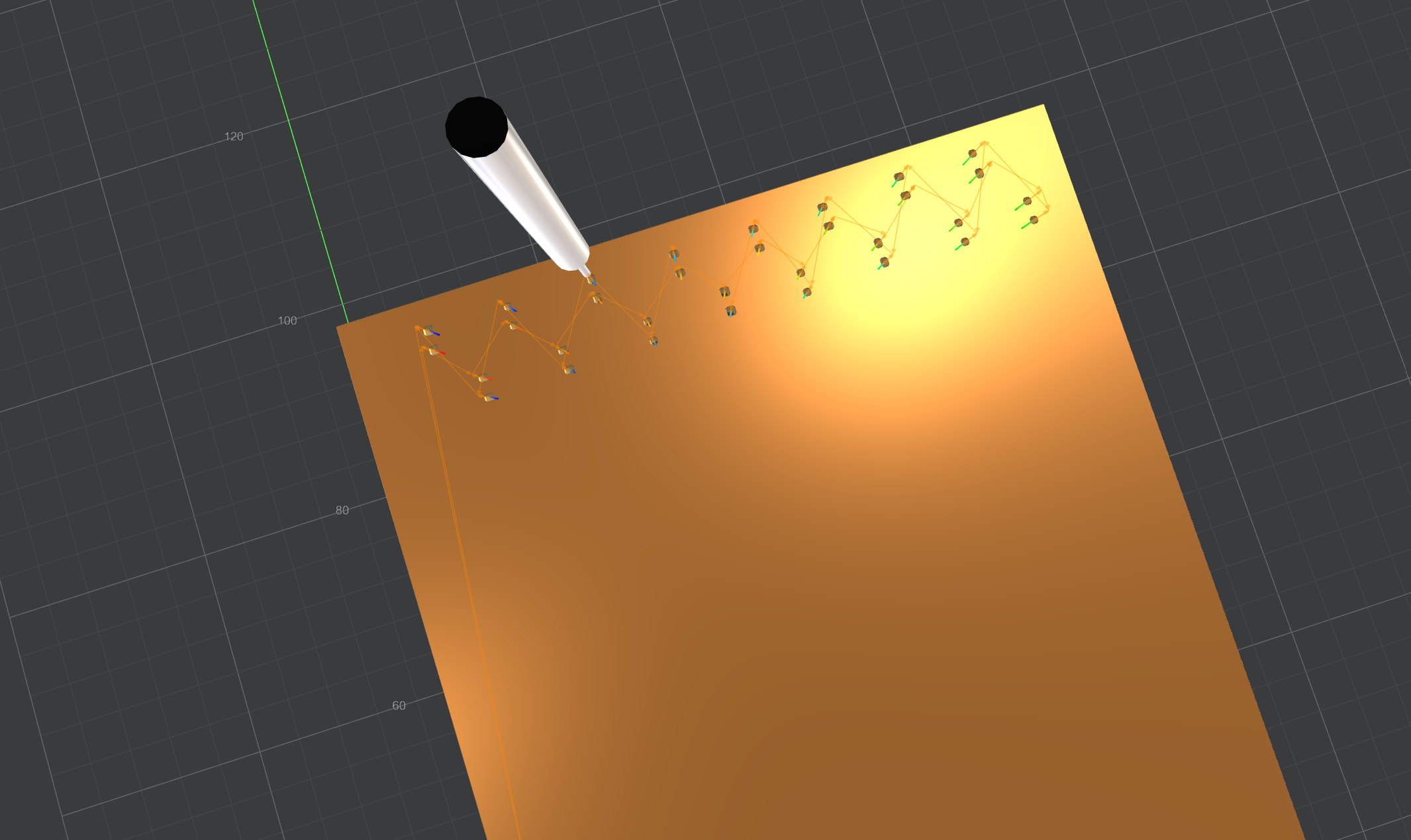
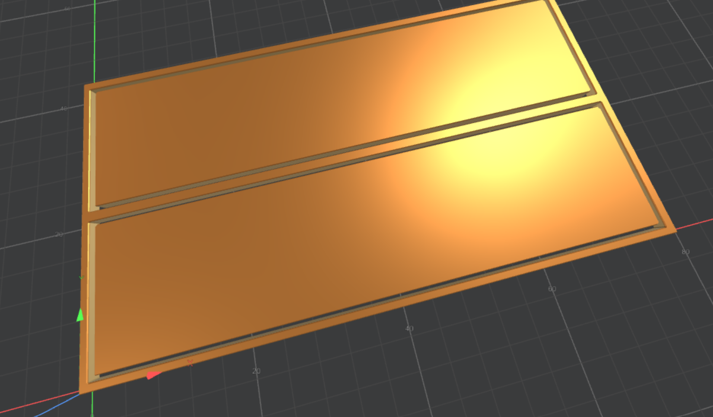
3D simulation view of the isolated logic traces on copper stock
3. Traces 3D Simulation: Visualizing the isolated logic paths on the virtual FR1 stock before sending the code to the mill.
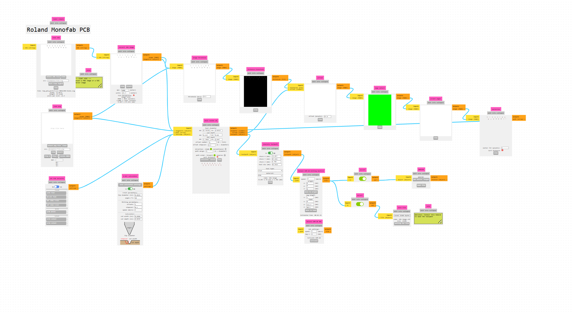
Full Roland Monofab PCB workspace workflow layout for the board edge cutout
4. Complete Workspace Layout: The complete node graph configuration in Mods CE managing the raw board vectors and dimensions for the edge.
Mods CE profile milling settings for the board outline cutout
5. Edge Cutout Configuration: Setting up the profile cutout parameters using a 0.792mm (1/32") mill bit to pass fully through the board substrate.
Mods CE parameters for through-hole via plunge drilling
6. Drilling Parameters: Adjusting the 2D raster plunge depth and tool diameter for the custom through-hole via arrays.
Drill file node flow configuration setup in Mods CE
7. Drill Node Flow: The full network graph mapped out specifically to calculate tool positioning for structural component holes.
3D simulated preview of the drilled hole matrix positions
8. Drill Matrix Simulation: A 3D preview confirming the exact mechanical plunge coordinates for the structural pin connections.
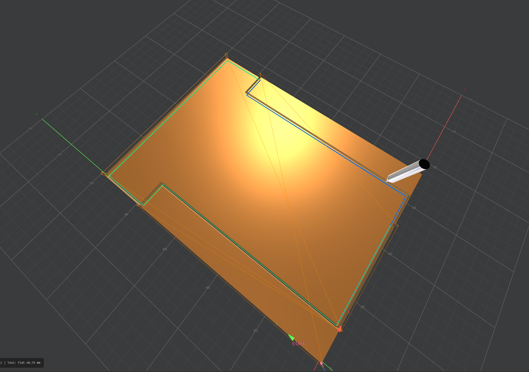
3D simulation view of the outer profile edge cutting path
9. Board Outline Simulation: The final outer perimeter toolpath simulation verifying the raw mechanical board profile.
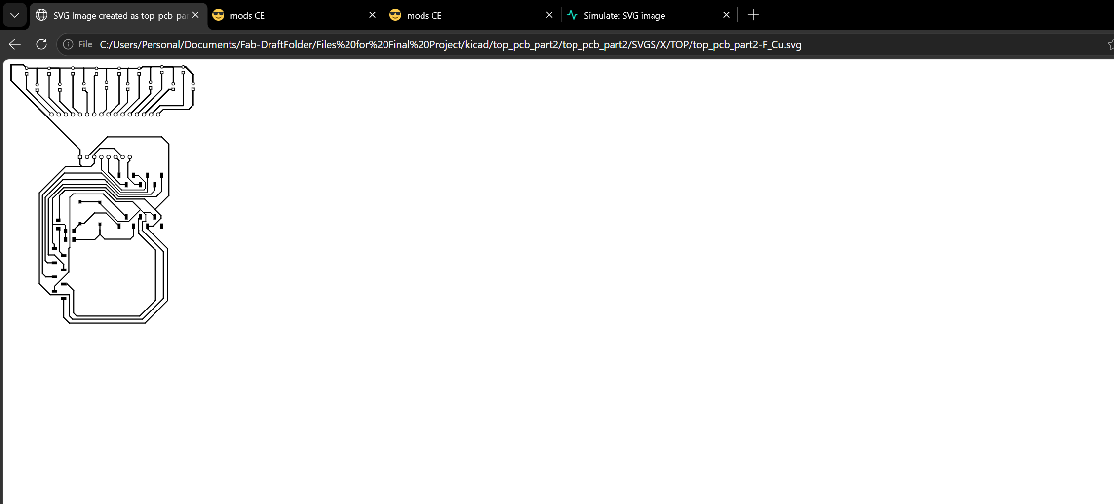
Raw SVG vector trace layout exported directly from KiCAD before refinement
10. Raw Vector Export: The clean, high-resolution SVG export straight out of KiCAD before any vector cleanup or final adjustments.
After Inkscape treatment
11. After Inkscape Treatment.
#### PCB Assembly
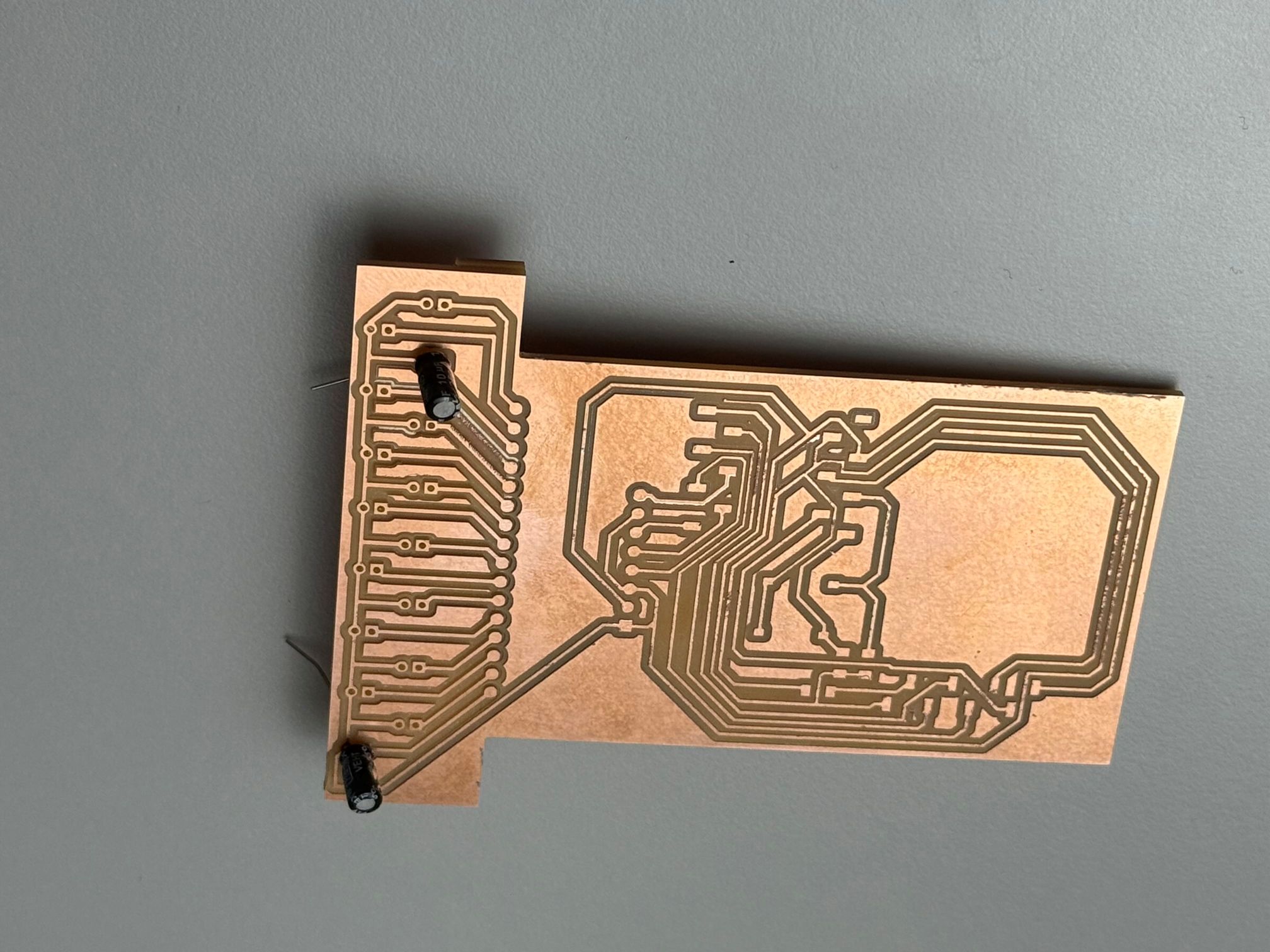
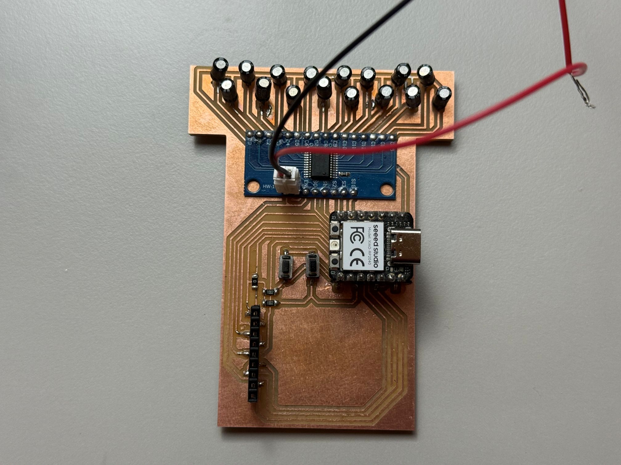
PCB assembly front view
Front view
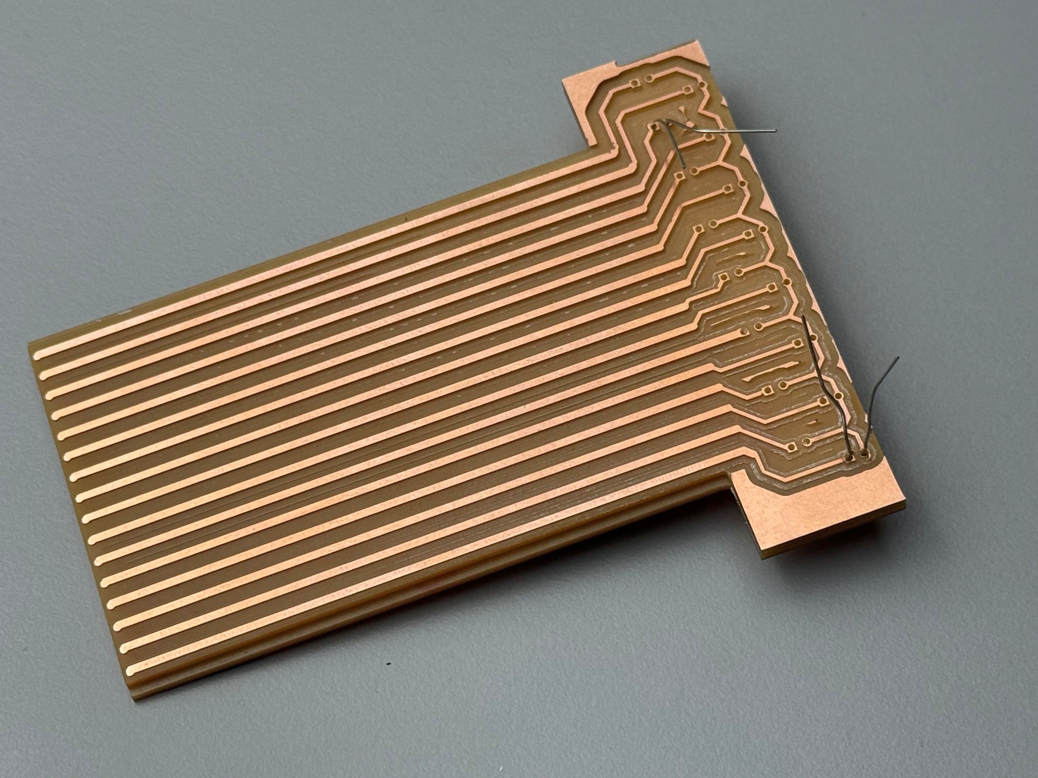
PCB assembly back view
Back view
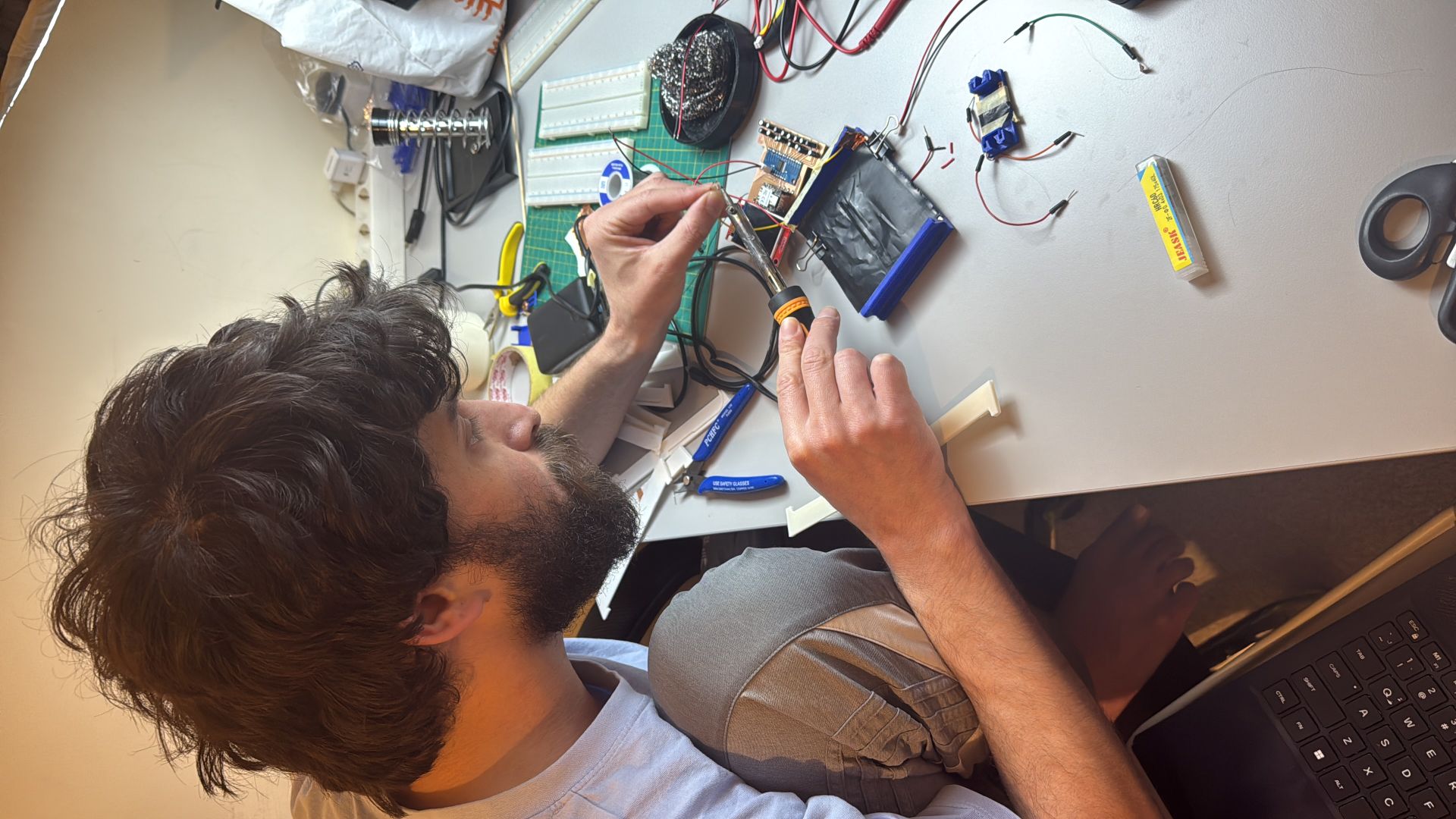
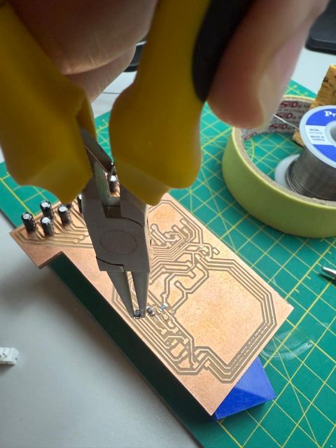
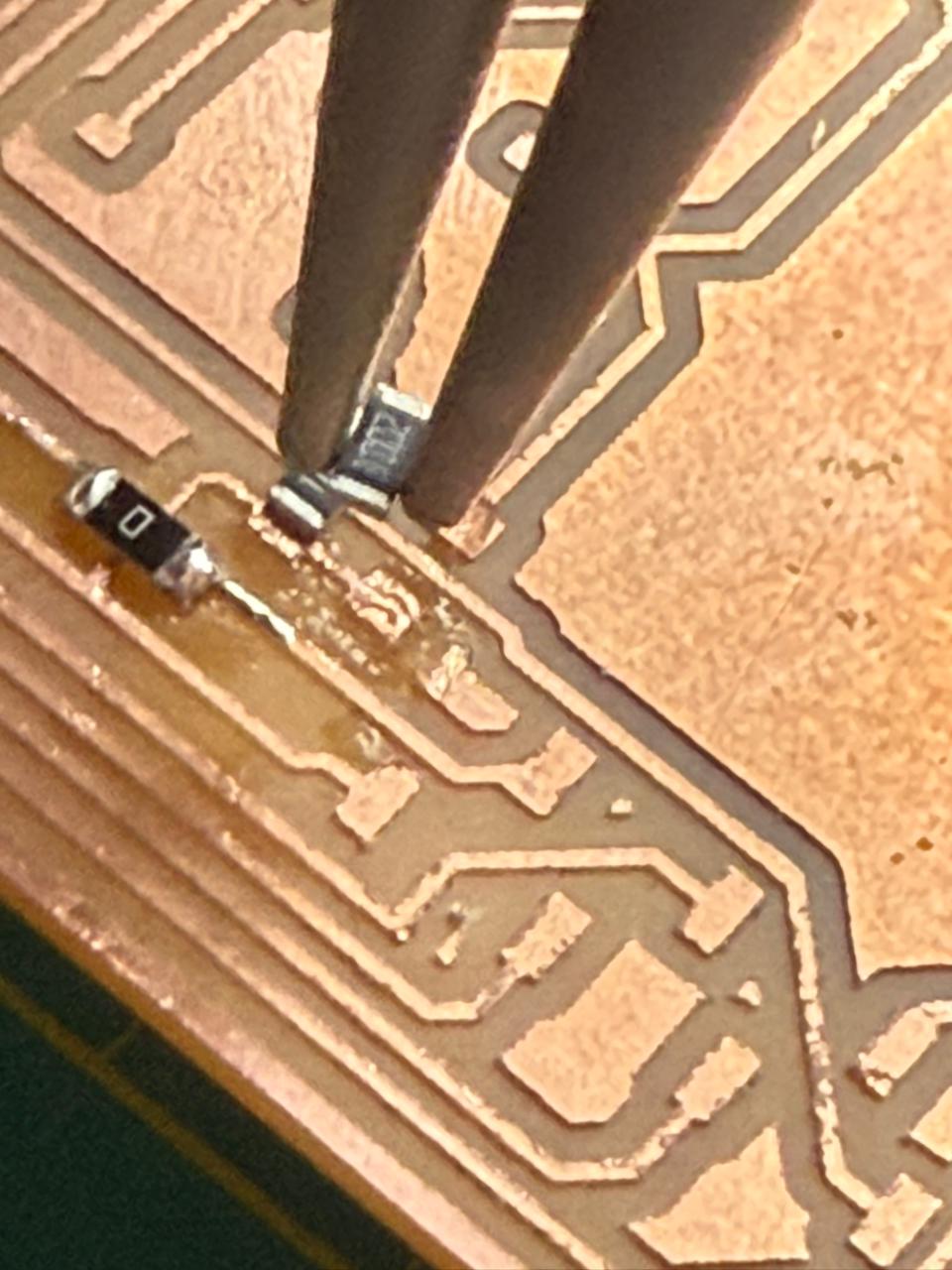
Soldering components
Soldering process
Soldering components close up
Soldering close-up
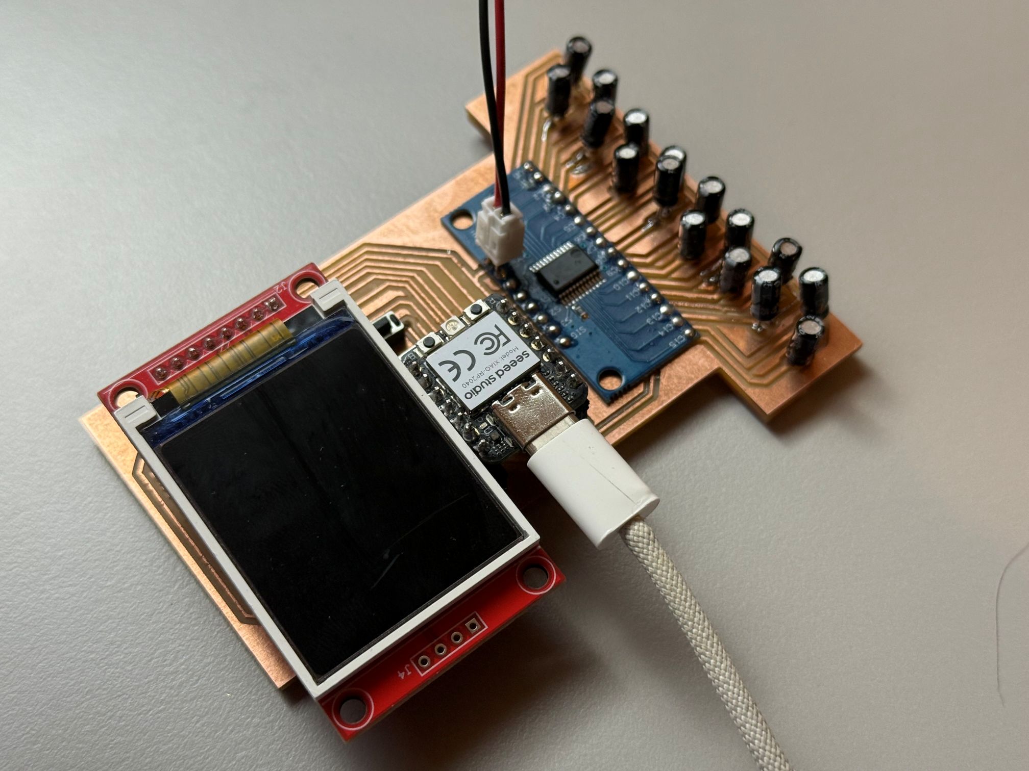
Final PCB assembly
Final assembly
Final PCB testing
Testing final board
0 ohm resistors
0 Ohm Resistors
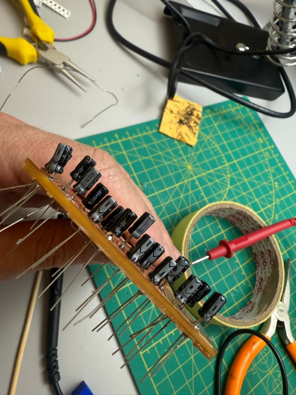
Capacitors
Capacitors
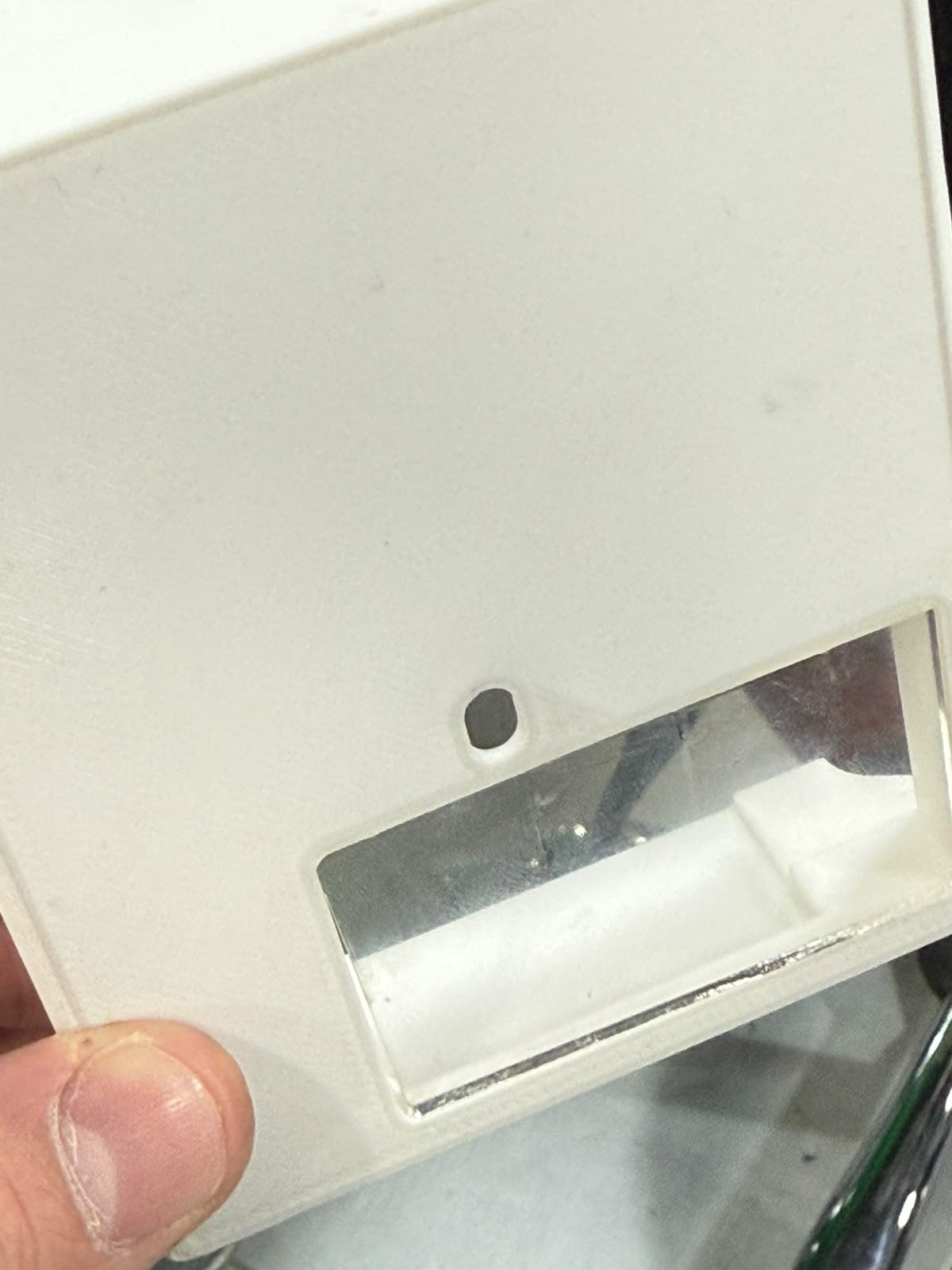
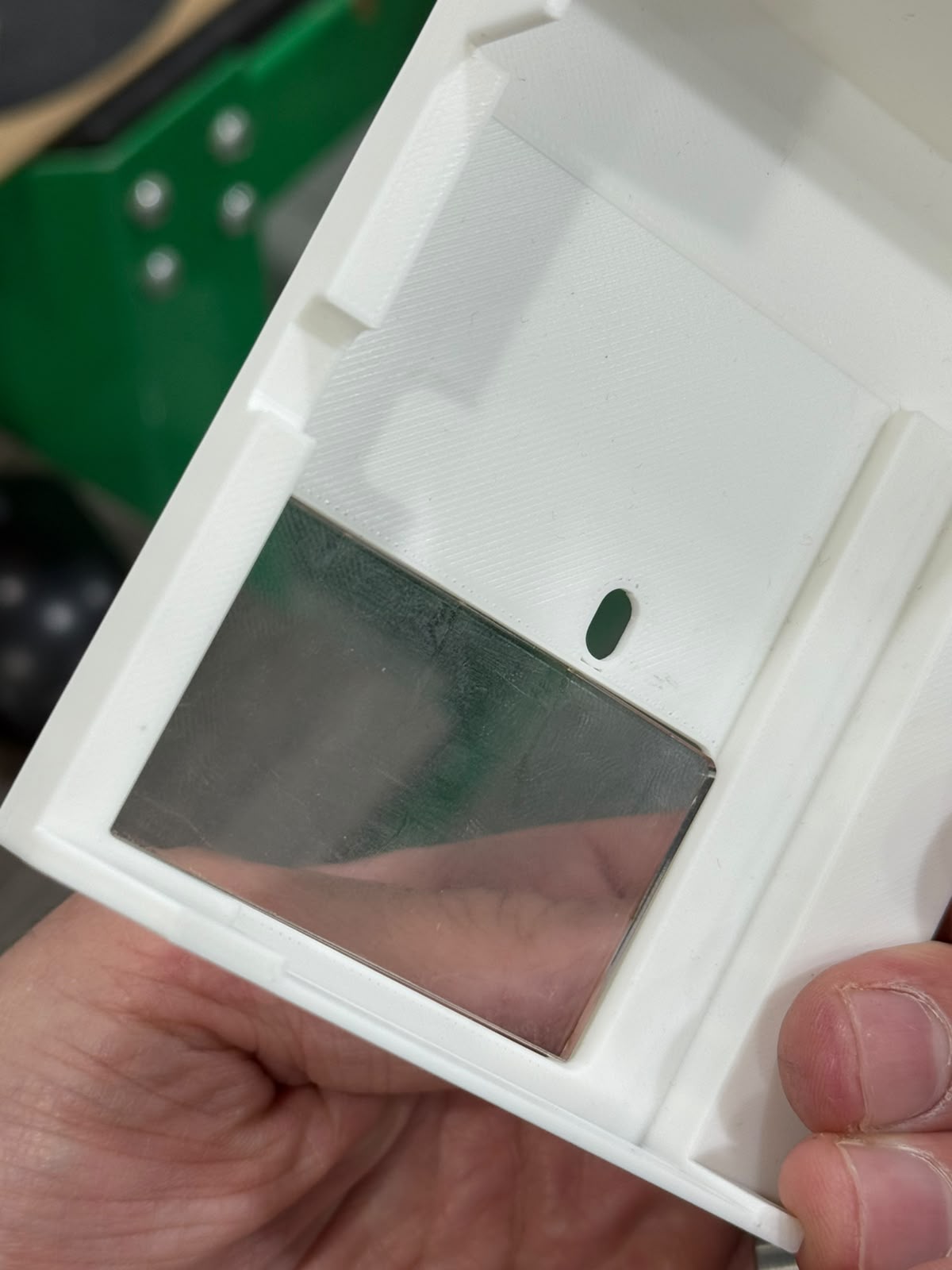
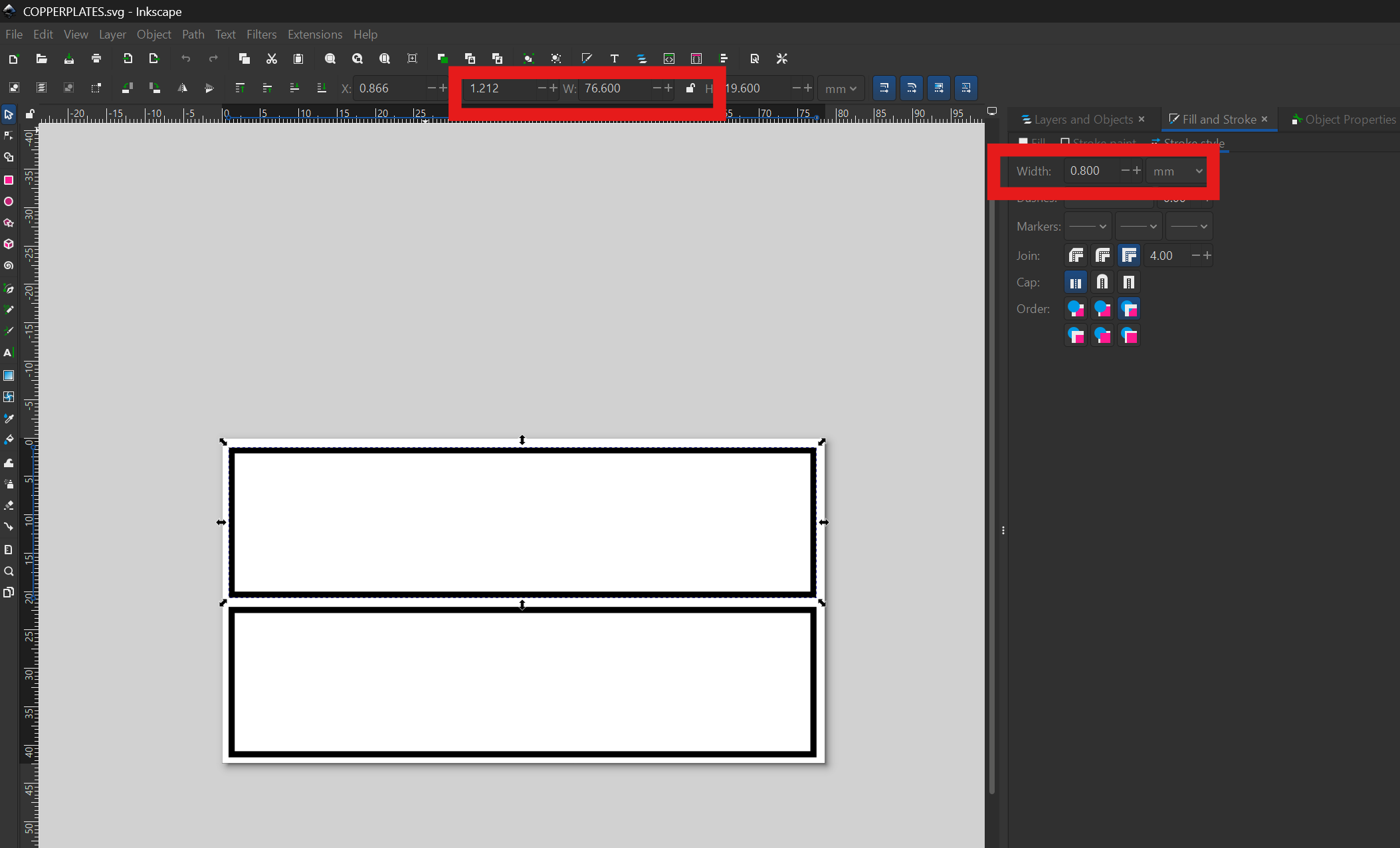
#### Subtractive Production - Milling the common ground and common vcc bars I used the Roland SRM-20 and the FR1 copper boards to mill out of them two rectangular-shaped common rails. The process here was different in terms of generating the toolpath ensuring the overall dimensions of the rectangle are preserved. I used Inkscape to account for the drill bit diameter as shown below: The dimensions of each copper piece needed were 75.8mm x 18.8mm. So first I drew the rectangle in the dimensions said, set the stroke width to 0.8mm (end mill diameter) and then modified the dimensions to add 0.8mm to the total width and total length so it compensates for that dimensional difference. I also used residual pieces from the copper board we cut earlier to produce the pieces. I used the electric saw to cut the pieces and follow the same mounting procedures of the plates explained in my previous week [8](week-eight.html). Finally, I generated the toolpaths as shown and cut the pieces using the 1/32" cutout tool setup.
Pro Tip / Warning

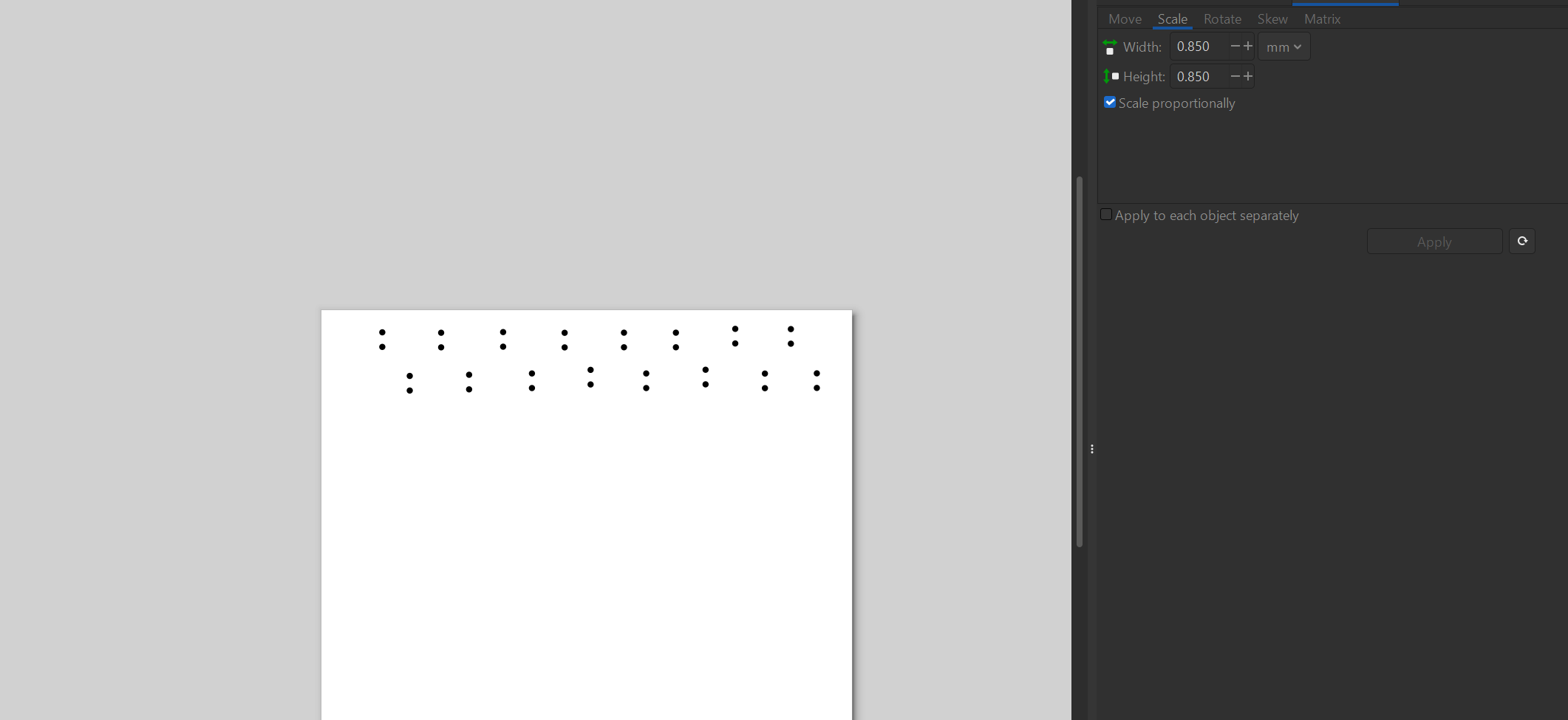
One major fabrication hurdle I hit was getting the toolpath to generate for the through-holes. In the raw vector export, the via holes were smaller than my 0.792mm (1/32") endmill, which caused Mods CE to completely ignore them during calculation.

To fix this without messing up the layout, I brought the SVG into Inkscape and used the Object Transform and Scale tool. By locking the proportions and scaling the hole vectors up to 0.85mm—making them explicitly larger than the tool diameter—I forced Mods to generate a clean, concentric drilling path. Because I scaled them uniformly using their bounding box centers, I cleared the tool path perfectly without losing their precise relative positions on the board grid.

Once the front layer was sorted, I repeated this exact same scaling and mirroring workflow for the back copper layer vectors to make sure everything aligned flawlessly back-to-back.
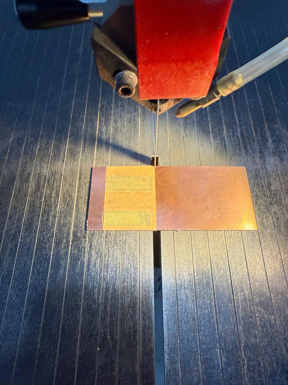
Cutting the residual piece
Inkscape post processing
Modsproject Settings
Toolpath preview
Toolpath preview
Copper pieces cut
Copper pieces cut
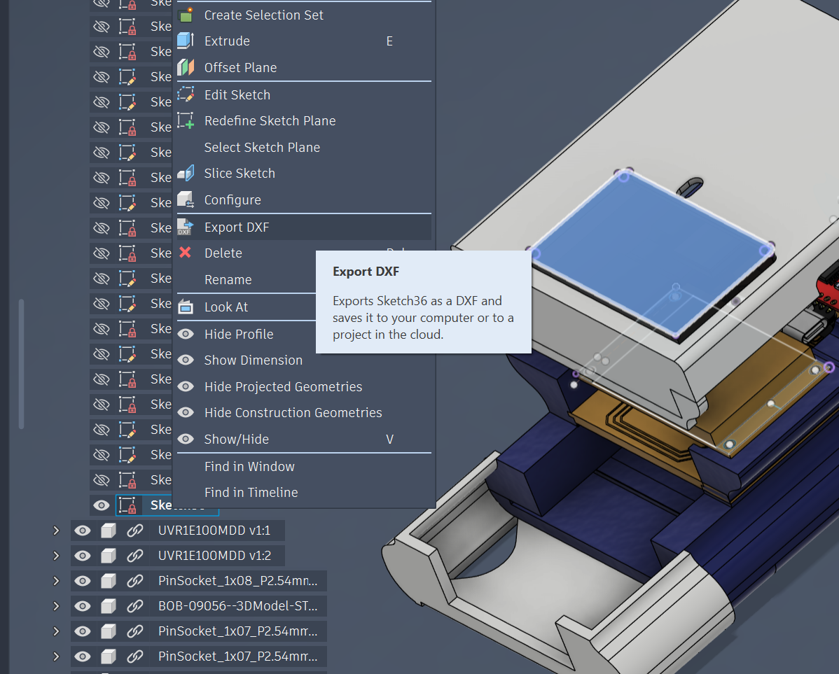
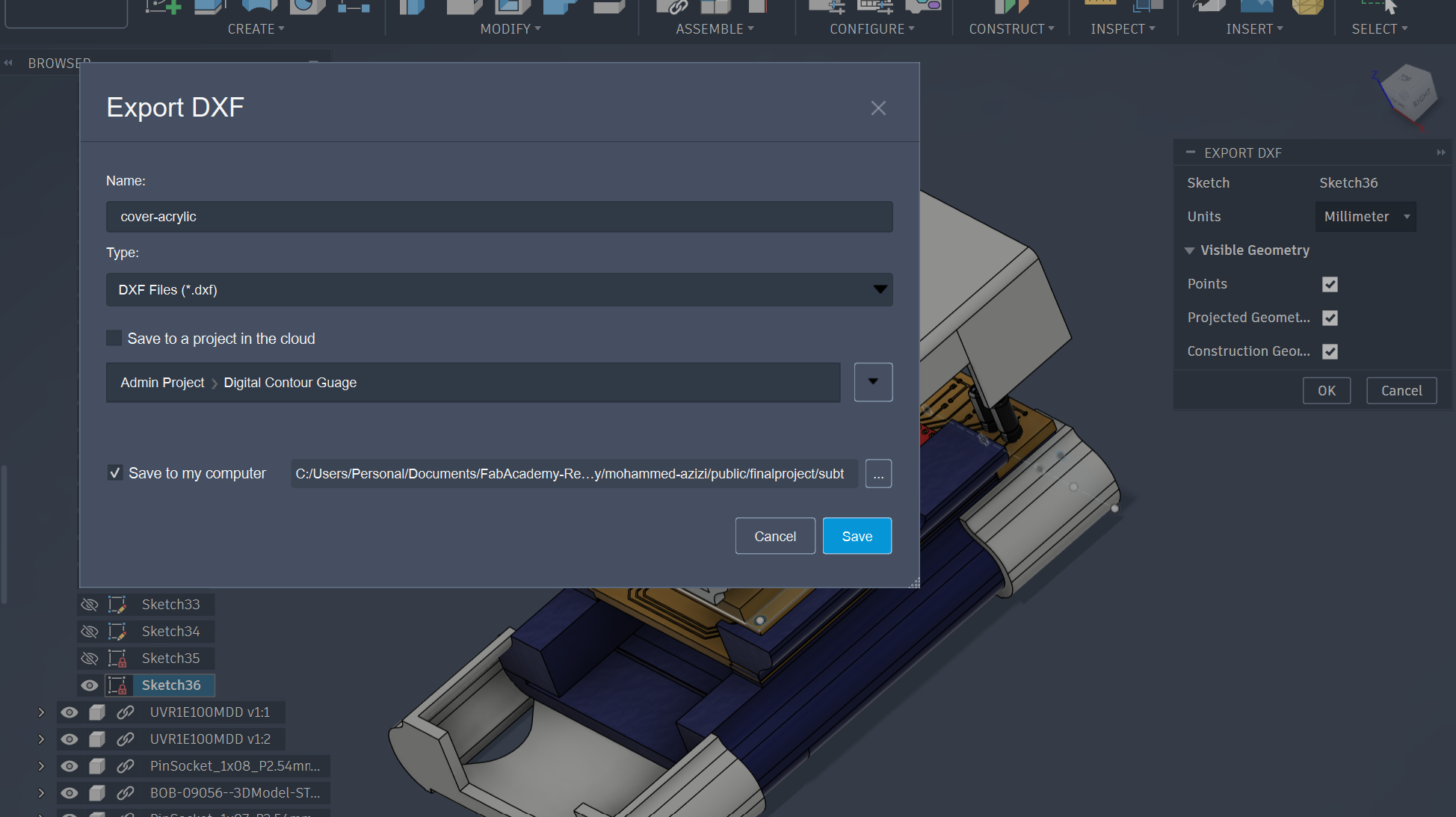
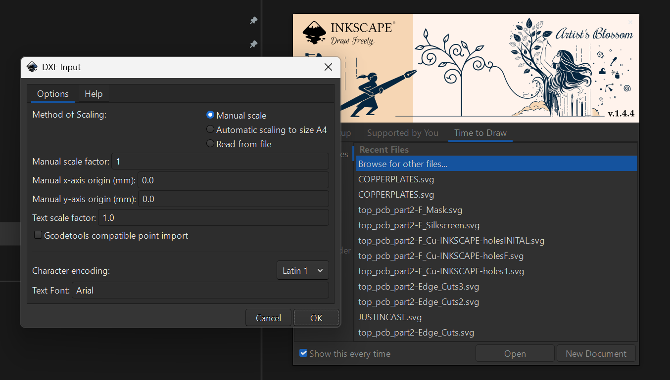
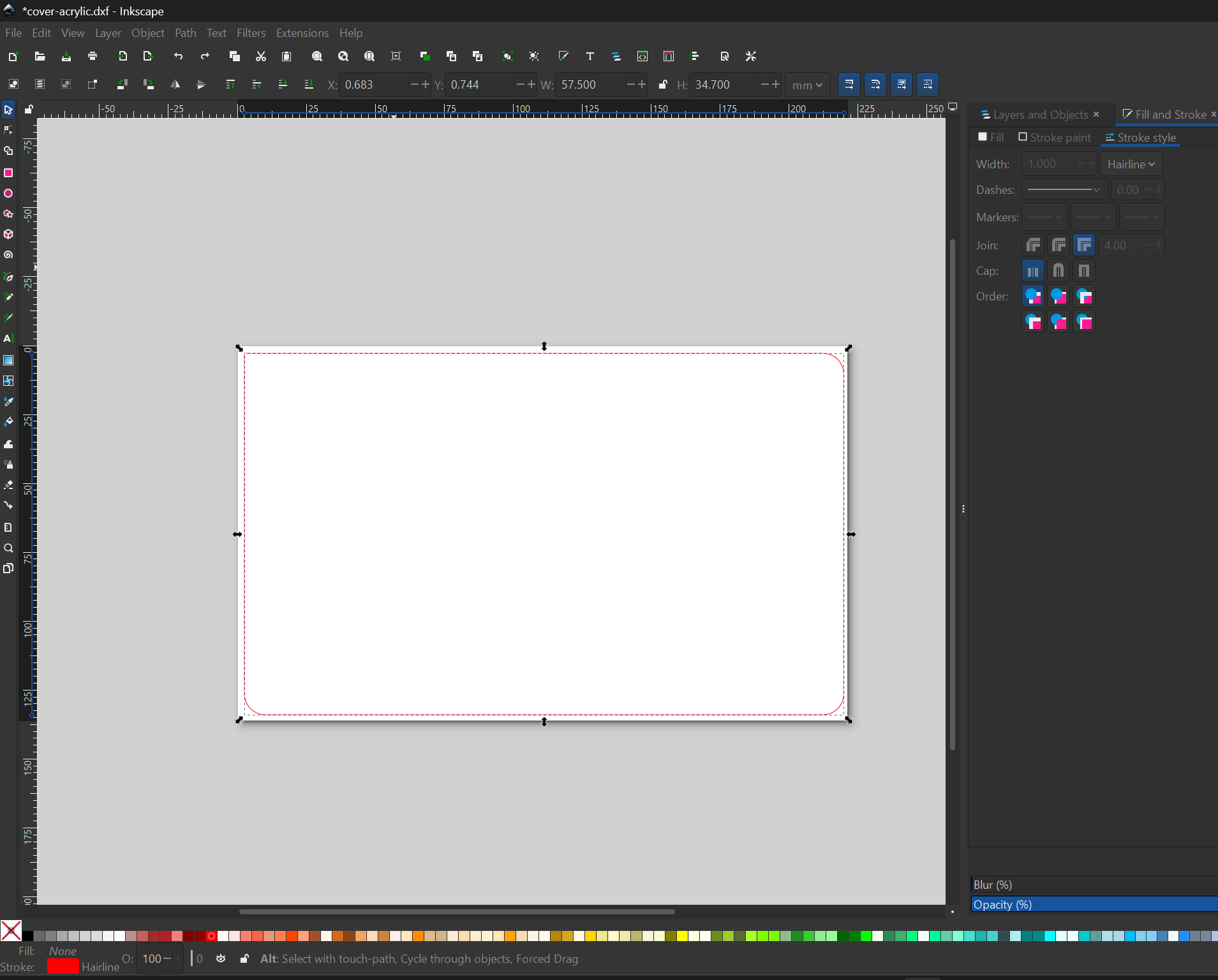
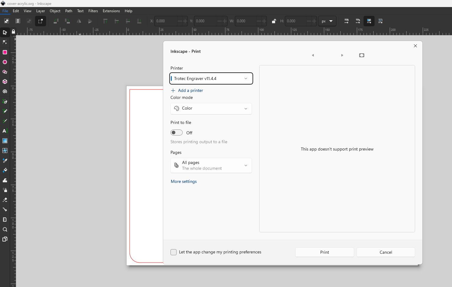
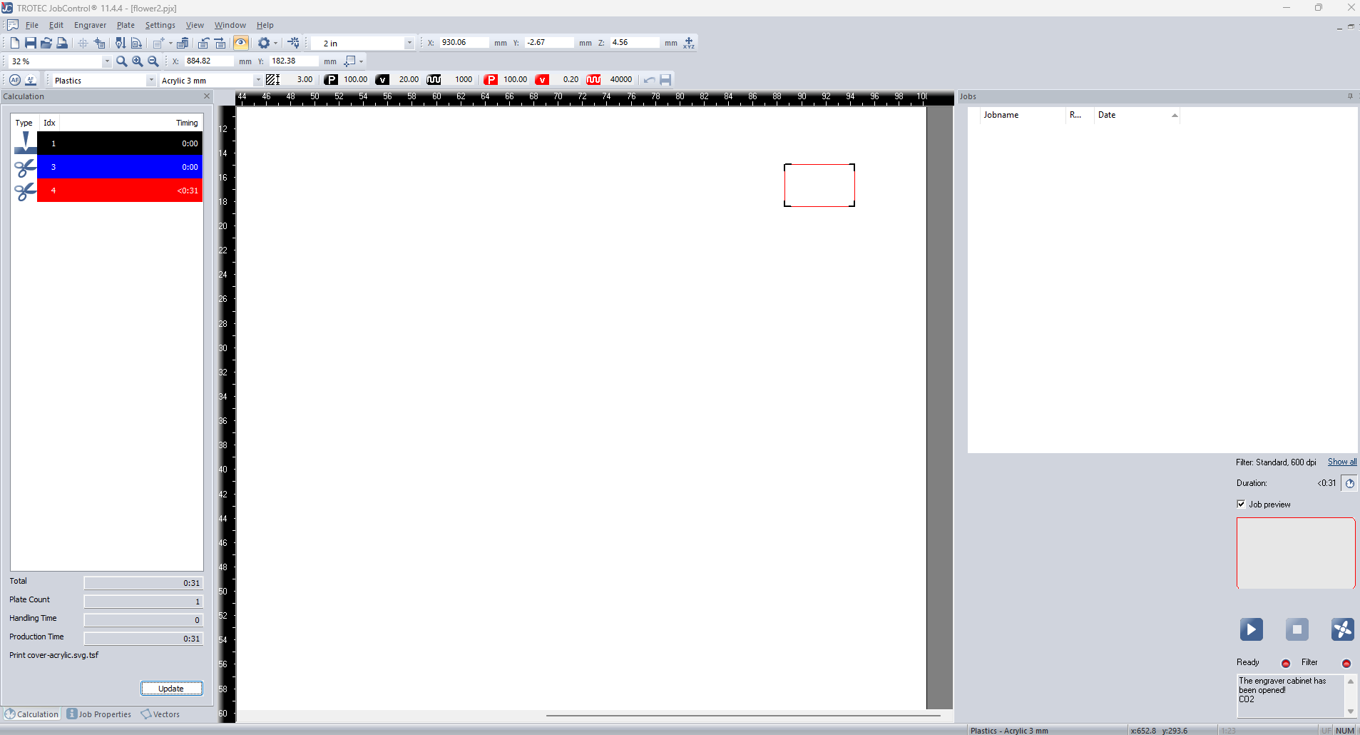
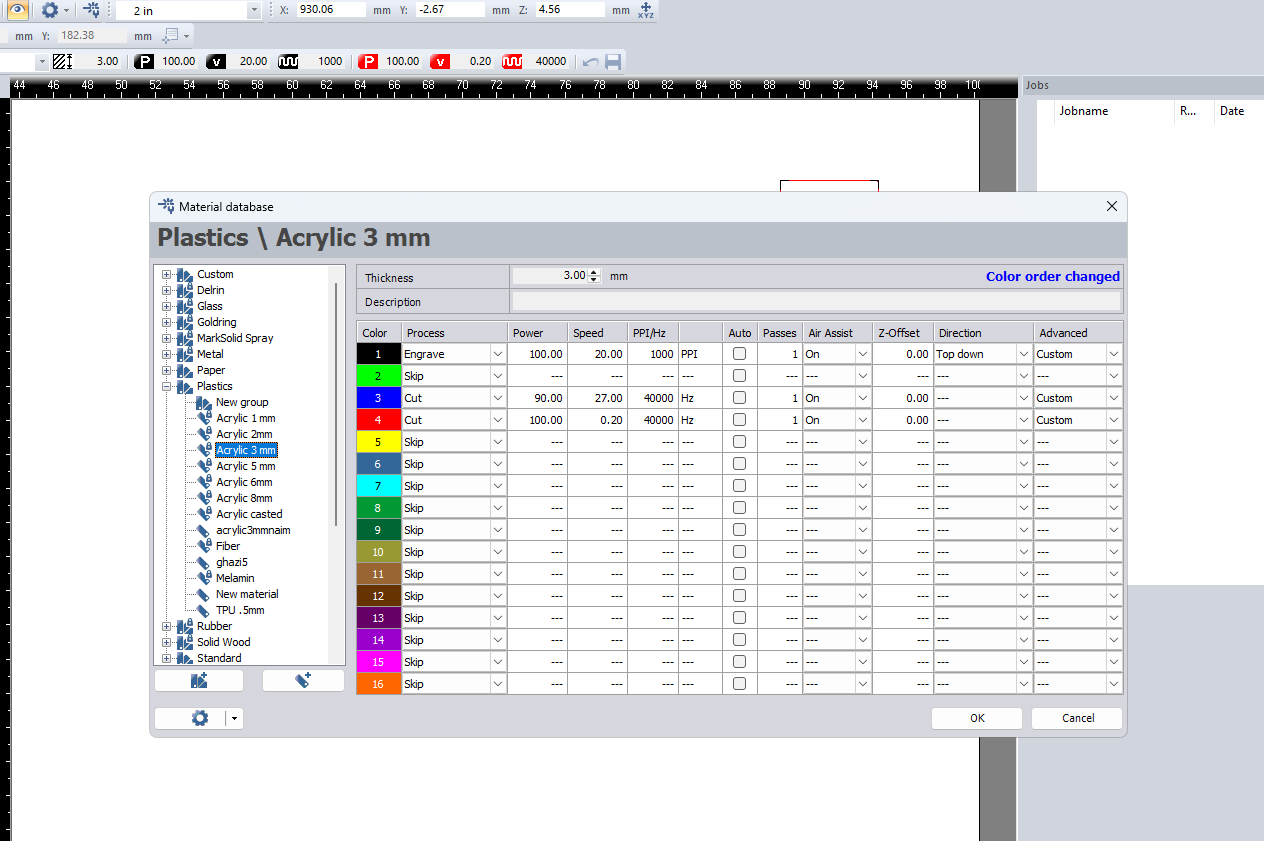
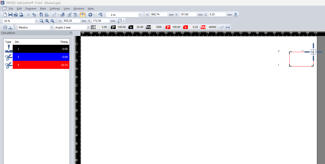
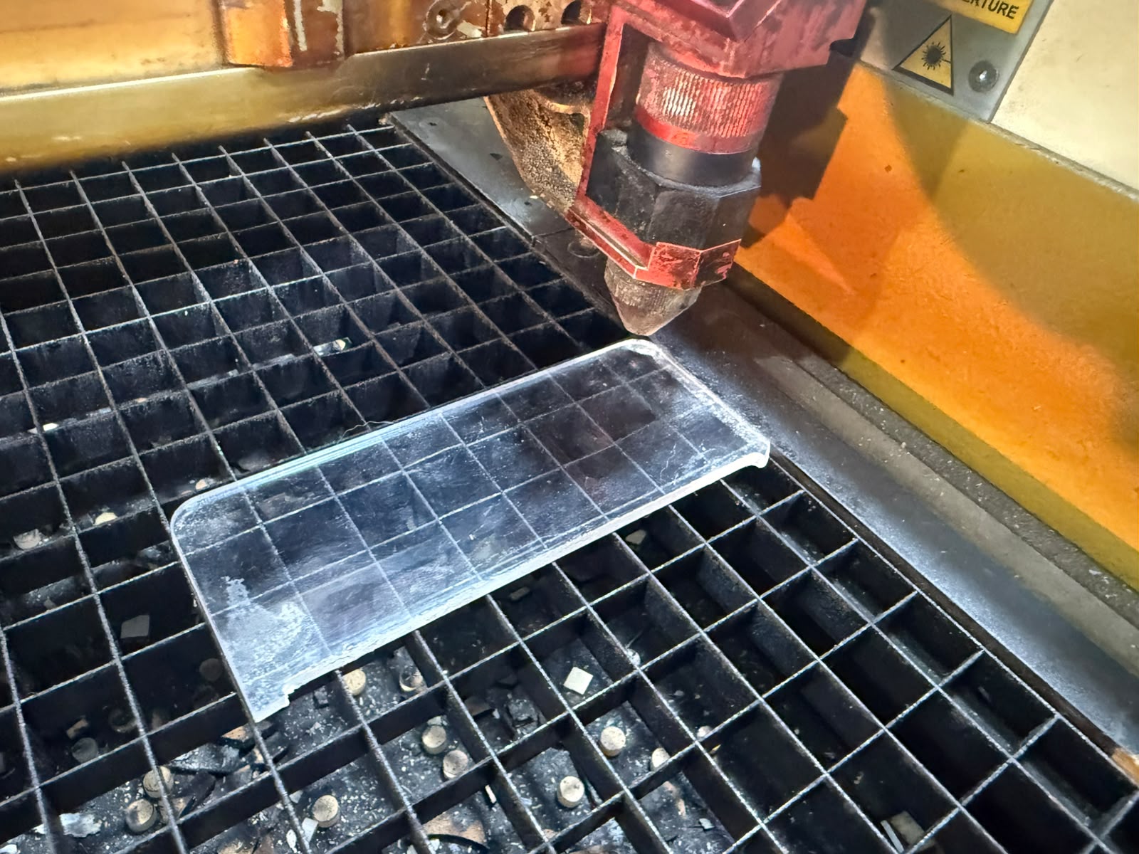
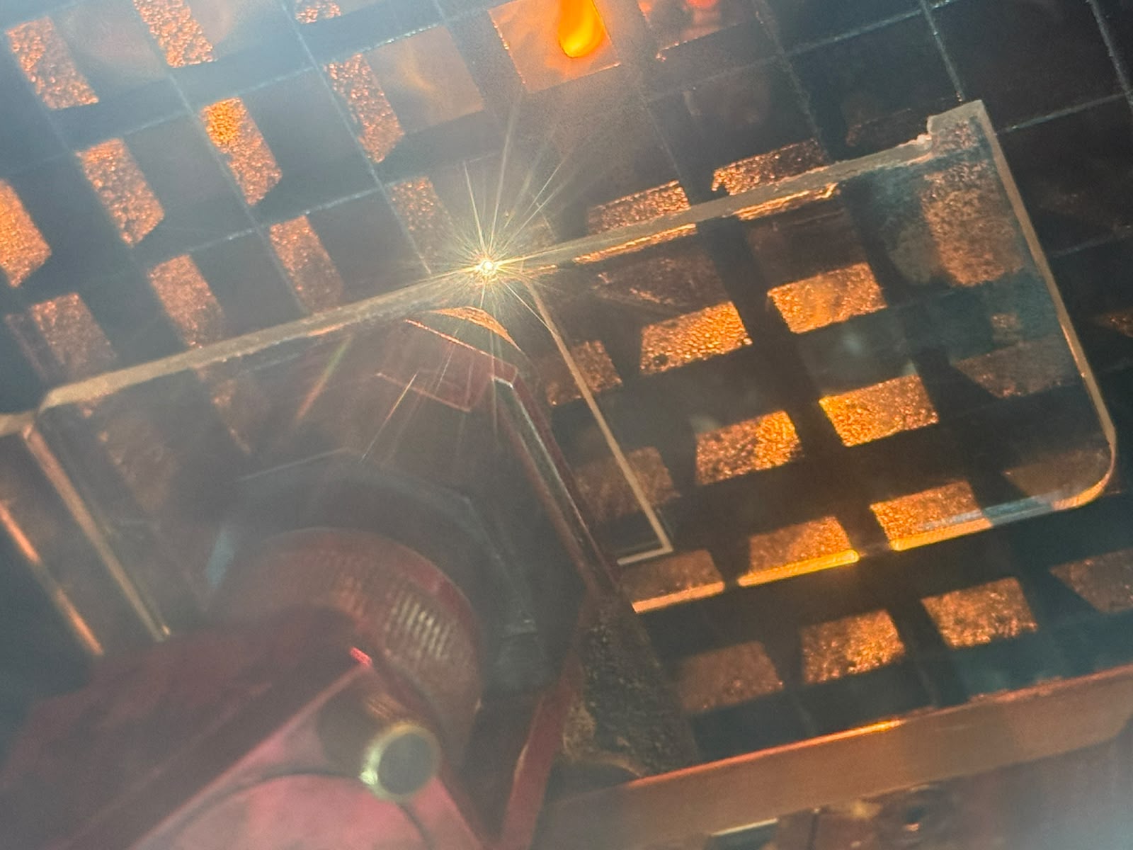
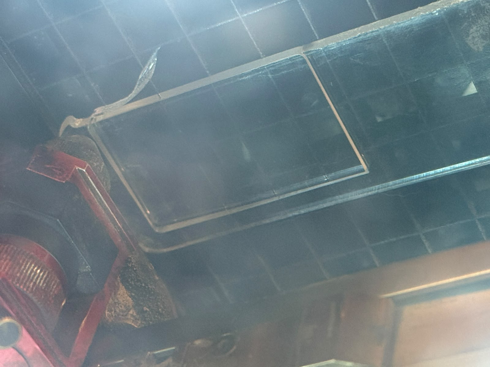
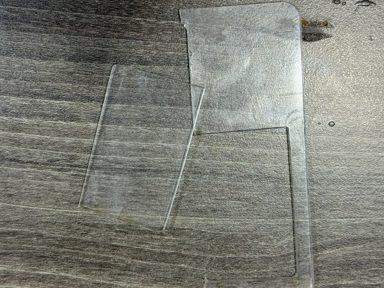
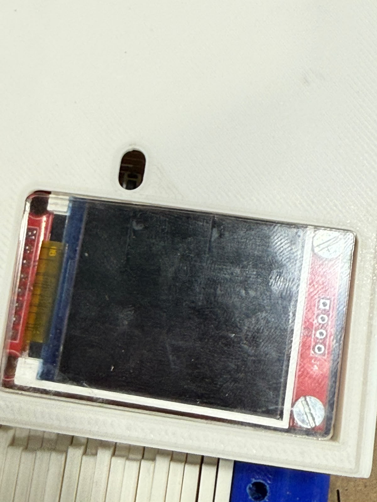
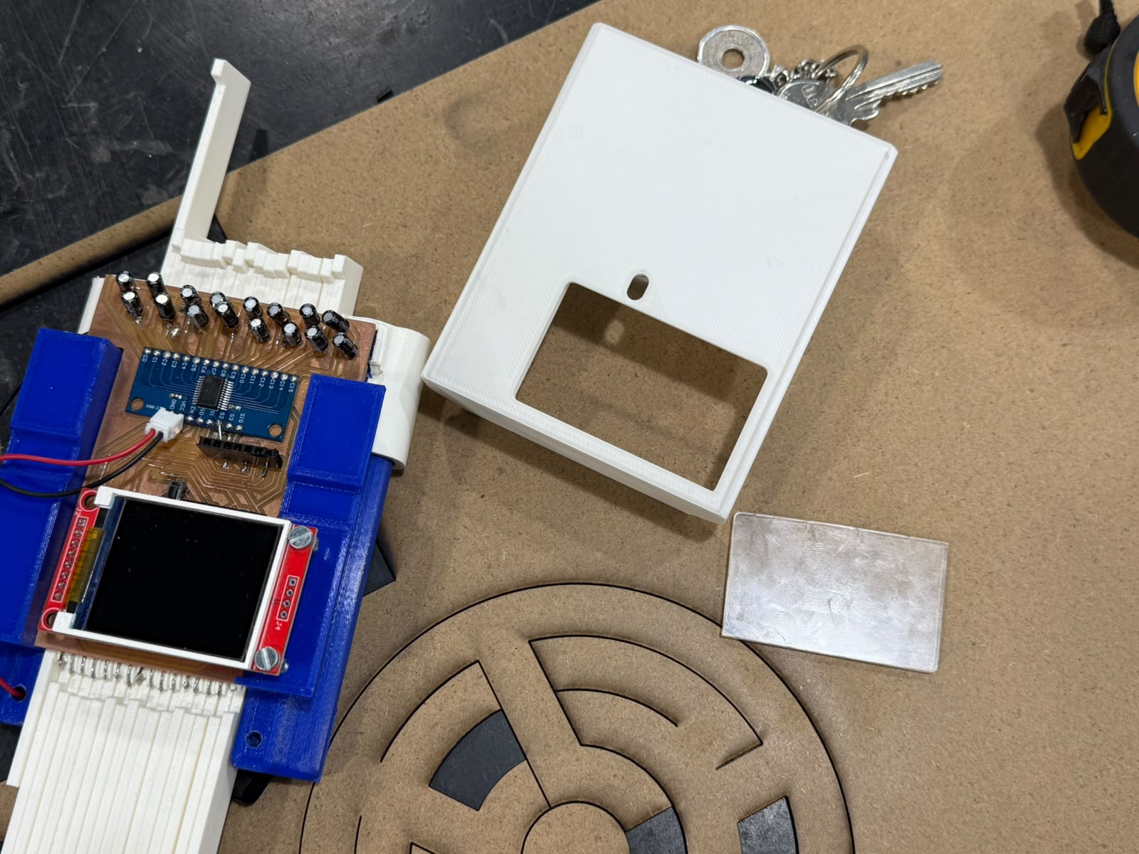
#### Subtractive Production - Acrylic Cover for the front face of the Digital Contour Gauge I used the trotec laser cutter and a risidual acrylic piece available to cut the front transparent cover of the digital contour guage, I first exported the gemoetry of the fit cover from fusion 360 as a dxf and then post processed it on inkscape. I finally proceeded to cut it using TROTECT JC and defining the suitable cutting settings for acrylic.

Bill of Materials & Cost

Electronics BOM (Final — 16-Tine Version)

# Category Component Qty Description Link / Reference
1 Core Electronics Seeed Studio XIAO RP2040 1 Main MCU (ESP32C3 as drop-in alternative) https://www.digikey.com/en/products/detail/seeed-technology-co-ltd/102010428/14672129
2 Core Electronics CD74HC4067 16-Ch Multiplexer 1 16 analog channels → single ADC pin https://mikroelectron.com/product/me-2912
3 Display 1.8" SPI TFT (ST7789 / ILI9341) 1 Color display; MOSI, CLK, CS, DC, RST, PWM backlight https://mikroelectron.com/product/me-12725
4 Sensor Milled FR1 Single-Sided Copper Board 2 Dual-layer stator — 16 vertical traces each https://store.bantamtools.com/products/pcb?variant=574277429
5 Sensor Velostat Conductive Plastic Sheet 1 Resistive layer for voltage division From the lab, no link found
6 Sensor Brass or Copper Busbars 2 VCC and GND rails along Velostat edges cut from the 5"X4" BOARDS https://store.bantamtools.com/products/pcb?variant=574277429
7 Mechanicals Custom Sliding Tines (PLA + wire) 16 FDM printed, 1mm conductive steel wire wiper From the lab / CPF Makerspace / Ultimaker Blue - PLA
8 Mechanicals Main Enclosure Chassis 1 FDM printed, white PLA From the lab / CPF Makerspace / Ultimaker White - PLA
9 Mechanicals M3 Bolts and Nuts 4 sets Structural fastening for main chassis setup From the lab inventory / CPF Makerspace
10 Power 3.7V LiPo Battery (500–1000 mAh) 1 Native pads on ESP32C3; TP4056 needed for RP2040 https://mikroelectron.com/product/me-14016
11 Passives 10µF 25V Capacitors (0805) 2 Noise filtering and via bridging https://mikroelectron.com/product/me-14685
12 Passives 10kΩ Resistors (1206) 2 Pull-down resistors for MUX SIG lines https://www.digikey.com/en/products/detail/yageo/RC1206FR-0710KL/728483
13 Passives 0Ω Resistors (1206) 1 PCB trace bridge https://www.digikey.com/en/products/detail/yageo/RC1206FR-070RL/5698945
14 Input Tactile SMD Push Buttons 2 Mode select and capture trigger From Mikroelektron / no public link / listed invoice image here 1, 2
15 Connectors 2.54mm Female Pin Headers 2 rows MCU docking, screen docking, board-to-board From Mikroelektron / no public link / listed invoice image here 1, 2
16 Connectors JST 2-Pin Headers 2 VCC/GND bridging to bottom copper layer From Mikroelektron / no public link / listed invoice image here 1, 2
### Mechanical & Filament BOM | Component | Qty | Notes | |---|---|---| | PLA Filament — White | 1 roll | Main chassis and structural parts | | PLA Filament — Blue | 1 roll | Tines and accent components | | 1mm Conductive Steel Wire | 1 roll | Cut and embedded into tine tips | | FR1 Copper Boards (120×250mm, single-sided) | 2 | PCB milling substrate | ### Under-Study / Alternative Components | Item | Specification | Role | Notes | |---|---|---|---| | Conductive PLA Filament | Standard 1.75mm | Alternative tine tip material | High resistance — requires software calibration | | 1.3" or 2.4" ST7789 SPI TFT | Larger format | Higher resolution display option | Requires SPI routing + PWM backlight pin | | LiPo + TP4056 Charger (RP2040 variant) | 3.7V, 500–1000mAh | Portable power for RP2040 | External charger module required | ### Cost Summary - **Electronics total:** approximately 50 USD (all sourced locally from MikroElektron, Amman, Jordan) - **Filament:** 15–20 JD per roll (available locally and in-lab) - **FR1 boards, fasteners:** available in the TechWorks lab - **No external procurement required** — all components obtained locally

## Applications & Implications ### Primary Use Case — Pipeline Inspection The DCG directly addresses the field workflow problem described in Section 1.2: - A pipe dent cross-section is captured in seconds rather than minutes - The profile is immediately rendered on-screen for visual confirmation - The DXF file is generated on the spot and can be inserted directly into an inspection report or opened in Fusion 360 / AutoCAD for dent strain calculation per ASME B31.8 - The result is shareable over Wi-Fi or USB without any manual redrawing or transcription
### Secondary Applications - **Rapid design replication:** Scan an irregular profile from an existing physical part and reproduce it exactly in CAD — useful for reverse engineering, heritage restoration, or custom fabrication. - **Architectural profiling:** Capturing cross-sections of moldings, cornices, or irregular structural members on-site. - **Tooling and jig verification:** Confirming that a machined or formed profile matches its design specification in the workshop, without a CMM. ### Who Can Build This Any Fab Lab with a 3D printer, a desktop PCB mill (Roland SRM-20 or equivalent), and access to locally available electronics can replicate this device. The total BOM cost is approximately 50 USD in electronics. The modular tine design means worn or damaged tines can be replaced individually without touching the electronics. All design files, firmware, and Python scripts are released as open source.
## Intellectual Property & Licensing ### License The Digital Contour Gauge is released under the **MIT License**. This was chosen deliberately: the mechanical contour gauge concept is not novel; what is being contributed is a specific implementation — the Velostat sandwich stator, the multiplexed tine architecture, the UART-to-DXF pipeline, and the integrated open-source design package. The MIT license allows maximum freedom for replication, modification, and commercial use, which aligns with the goal of making this tool accessible to engineers and Fab Labs worldwide. ## Licensing Strategy ### Chosen License: The MIT License For the initial rollout of this project, particularly the software implementation and firmwares, I have chosen to adopt the **MIT License**. This choice directly supports my plan to launch a Kickstarter campaign and build an open developer community. ```text MIT License Copyright (c) 2026 MOHAMMED ABDULRAHMAN IZZAT AZIZI Permission is hereby granted, free of charge, to any person obtaining a copy of this software and associated documentation files (the "Software"), to deal in the Software without restriction, including without limitation the rights to use, copy, modify, merge, publish, distribute, sublicense, and/or sell copies of the Software, and to permit persons to whom the Software is furnished to do so, subject to the following conditions: The above copyright notice and this permission notice shall be included in all copies or substantial portions of the Software. THE SOFTWARE IS PROVIDED "AS IS", WITHOUT WARRANTY OF ANY KIND, EXPRESS OR IMPLIED, INCLUDING BUT NOT LIMITED TO THE WARRANTIES OF MERCHANTABILITY, FITNESS FOR A PARTICULAR PURPOSE AND NONINFRINGEMENT. IN NO EVENT SHALL THE AUTHORS OR COPYRIGHT HOLDERS BE LIABLE FOR ANY CLAIM, DAMAGES OR OTHER LIABILITY, WHETHER IN AN ACTION OF CONTRACT, TORT OR OTHERWISE, ARISING FROM, OUT OF OR IN CONNECTION WITH THE SOFTWARE OR THE USE OR OTHER DEALINGS IN THE SOFTWARE. ``` ### Understanding the MIT License The MIT License is a **permissive open-source license**. This means: * **High Flexibility:** Anyone can download, modify, distribute, and even sell the software or use it in their own custom systems without needing to pay royalties. * **Community Adoption:** By lowering the barrier to entry, it encourages hackers, reverse-engineers, and makers to build custom plugins or add-ons for the Digital Contour Gauge ecosystem. * **Liability Protection:** Crucially, it includes an "As-Is" clause, protecting me from legal liability if someone uses the code in an unexpected context. ### Alternative Licensing Models Considered While the MIT license is fantastic for generating goodwill and developer adoption on platforms like Kickstarter, I evaluated alternative frameworks to balance my commercial ambitions: * **Dual-Licensing Model (AGPL + Commercial):** I could release the core source code under a copyleft license like the GNU AGPLv3. This forces any company modifying my code for a cloud dashboard or a proprietary network to release their changes back to the open community. If a gas utility provider wants to keep their code completely private and proprietary, they would be required to buy a paid **Commercial License** from me. This is a highly viable secondary step as the project matures. * **Hardware Specific Licenses (CERN-OHL or CC BY-NC-SA):** While software uses MIT, my structural CAD files and physical PCB layouts can utilize a license like **CC BY-NC-SA** (Creative Commons Attribution-NonCommercial-ShareAlike). This allows individual makers to fabricate their own replacement housings, but legally bars industrial competitors from manufacturing and selling my exact hardware design commercially without direct authorization. ### What Is Being Released | Asset | Format | Location | |---|---|---| | Full enclosure + tine 3D models | `.f3z`, `.f3d`, `.stl` | Fab Academy student page / files | | KiCAD PCB project | `.kicad_pcb`, `.sch`, Gerbers | Fab Academy student page / files | | Firmware | `.ino` (Arduino framework) | Fab Academy student page / files | | Python data pipeline | `.py` (pyserial, ezdxf) | Fab Academy student page / files | | Presentation slide | `presentation.png` (1920×1080) | Root directory | | Presentation video | `presentation.mp4` (1080p) | Root directory |

## Reflection & Future Work ### What Worked - The **Velostat sandwich stator** is an elegant sensing solution — inexpensive, locally sourceable, and mechanically simple. The voltage divider behavior is clean and predictable. - The **dual-layer FR1 PCB as a functional sensor substrate** (not just as a logic board) was a novel application that worked exactly as simulated. - The **UART → Python → DXF pipeline** is robust and produced correct CAD geometry from the first successful run. - The **modular tine design** — individual tines replaceable without disassembling the core electronics — proved its value during the multiple prototype iterations. - **Local sourcing was fully achieved** — no component required international procurement. ### What Was Hard - **KiCAD routing** on a mechanically constrained board with high trace density required three full routing iterations before a viable solution was found. - **Embedding conductive material in 3D-printed tines** required a print-pause protocol that was fiddly to execute consistently across 16 tines. - **Velostat clamping sensitivity** — small variations in clamping pressure across the sheet produce measurable ADC offset. Consistent mechanical clamping is critical and was the hardest thing to control in assembly. - **COM port conflicts** between Arduino IDE and the Python listener caused significant debugging time early in the communication development. - **Analog noise on the ESP32C3** required more aggressive software filtering than anticipated; the RP2040 would have been cleaner for this application. ### Roadmap — Future Iterations - Scale from 16 to 32 tines (PCB routing strategy now understood) - Bluetooth / wireless DXF export directly from the device — eliminate the laptop dependency - Standalone mobile app to replace the Python script - Onboard calibration routine in firmware (auto-zero and span calibration) - Enclosure ruggedization: IP54-rated gasket seal for field use in dusty or damp environments - Alternative sensing investigation: hall-effect linear sensors for higher resolution and no physical contact wear

12. Files & References

## Project Summary & Presentation This section indexes presentation-ready resources for the Fab Academy final review.
DCG Final Project Presentation Slide
Presentation slide — 1920×1080 summary for Fab Academy 2026 Final Review.
Presentation video — full project walkthrough including live hardware demo.