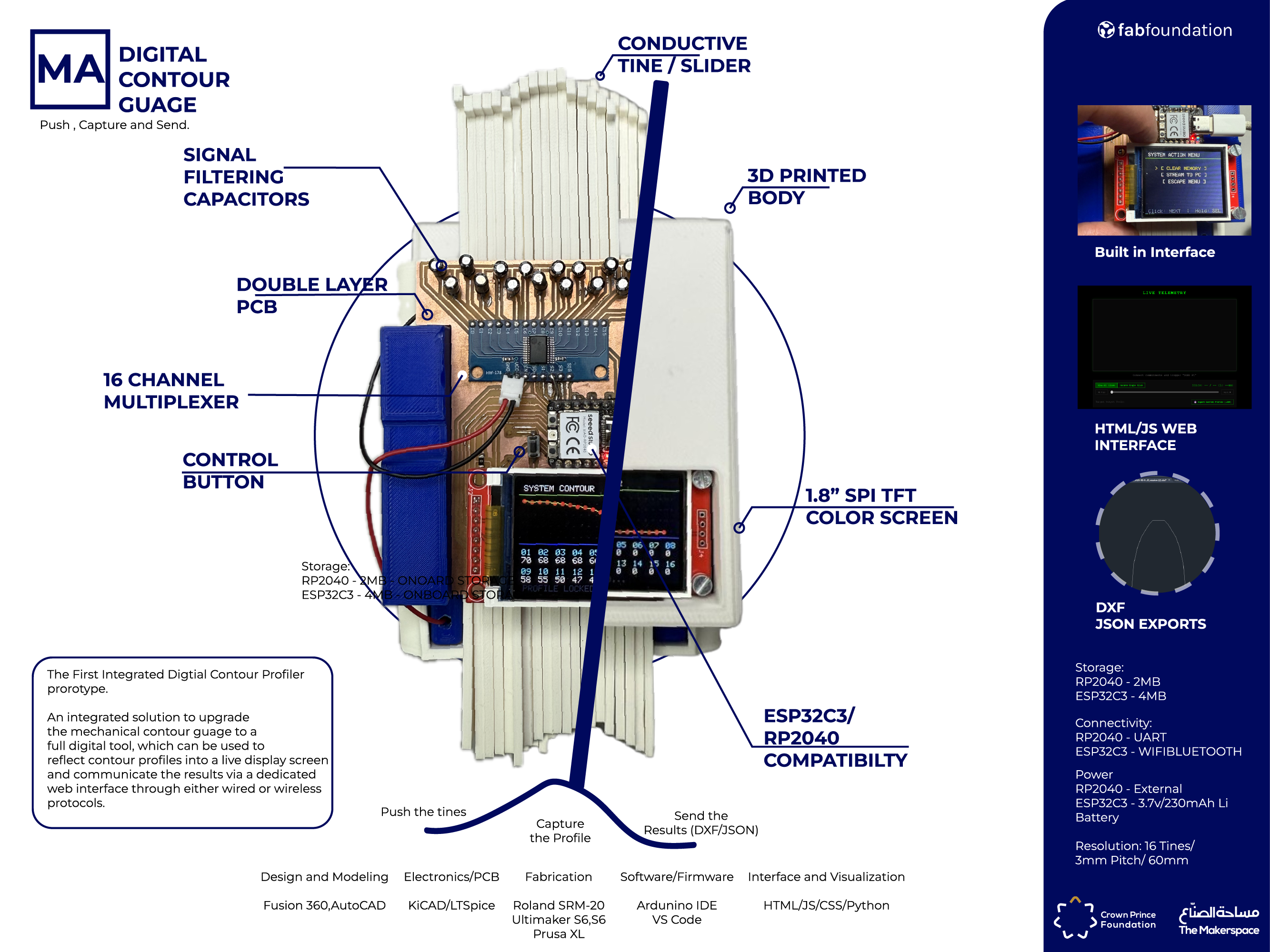
A tightly optimized hardware-firmware vertical architecture engineered for the Digital Contour Gauge.
## Research and Introduction
The Digital Contour Guage project comes from my personal experience and encounters where utilizing a simple tool can enhance engineering
workflows , and the current solutions provided to date do not tackle directly creating a robust solution to acheive that, more details can be found
on my [final project](dcg.html) page.
For this week I tried to define the system integrations and identify early on issues before production, to which I arrived to the summarized conclustions
1) My DFM checklist:
- 3D Modeled parts with minimal overhangs and supports , optimized files (70%)
- Defining BOM and off the shelf materials to avoid external depencancy or custom made parts (80%)
- Fastner reduction and elimination of threaded assemblies (50%)
- Alternative parts and spare parts availability (70%)
2) My overall design progress
-conceptual design phase (100%)
-preliminary design phase (40%)
-Detailed final design (5%)
My detailed workflows can be found my Final Project page [here](../finalproject.html)
## Conceptual Design Phase
During this phase I was focused to define a working proof of concept using on the shelf materials and readapting the existing mechanical model of the digital
contour gauge. This goal was to identify my parts and components in my preliminary design and test out the electronics using basic electronic components.
Below is a video of me testing out the proposed concept of the tine movement (moving arm/leg) over a velostat sheet,which as two copper tape pieces soldered to
wires which provide the voltage and gnd common busbars (mockup). I connected everything through wires, and I identified what wires I need to completely integrate
in my PCB and what wires I should keep.
In the video it shows the wires connected from the tine, a conductive copper strip acting as a bridge between the contact point on the velostat and the input wire
connected to the breadbaord on the RP2040 pins, this also is part of my work in weeks 9,10 and 11.
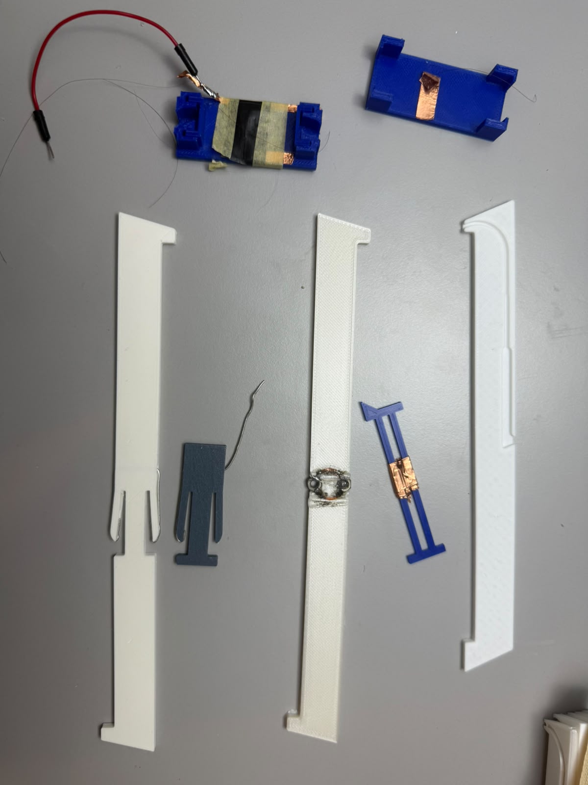
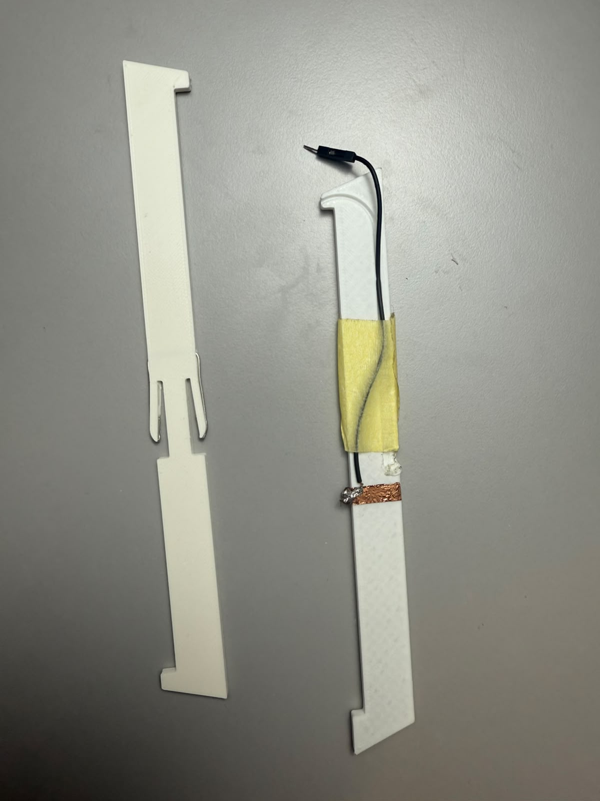
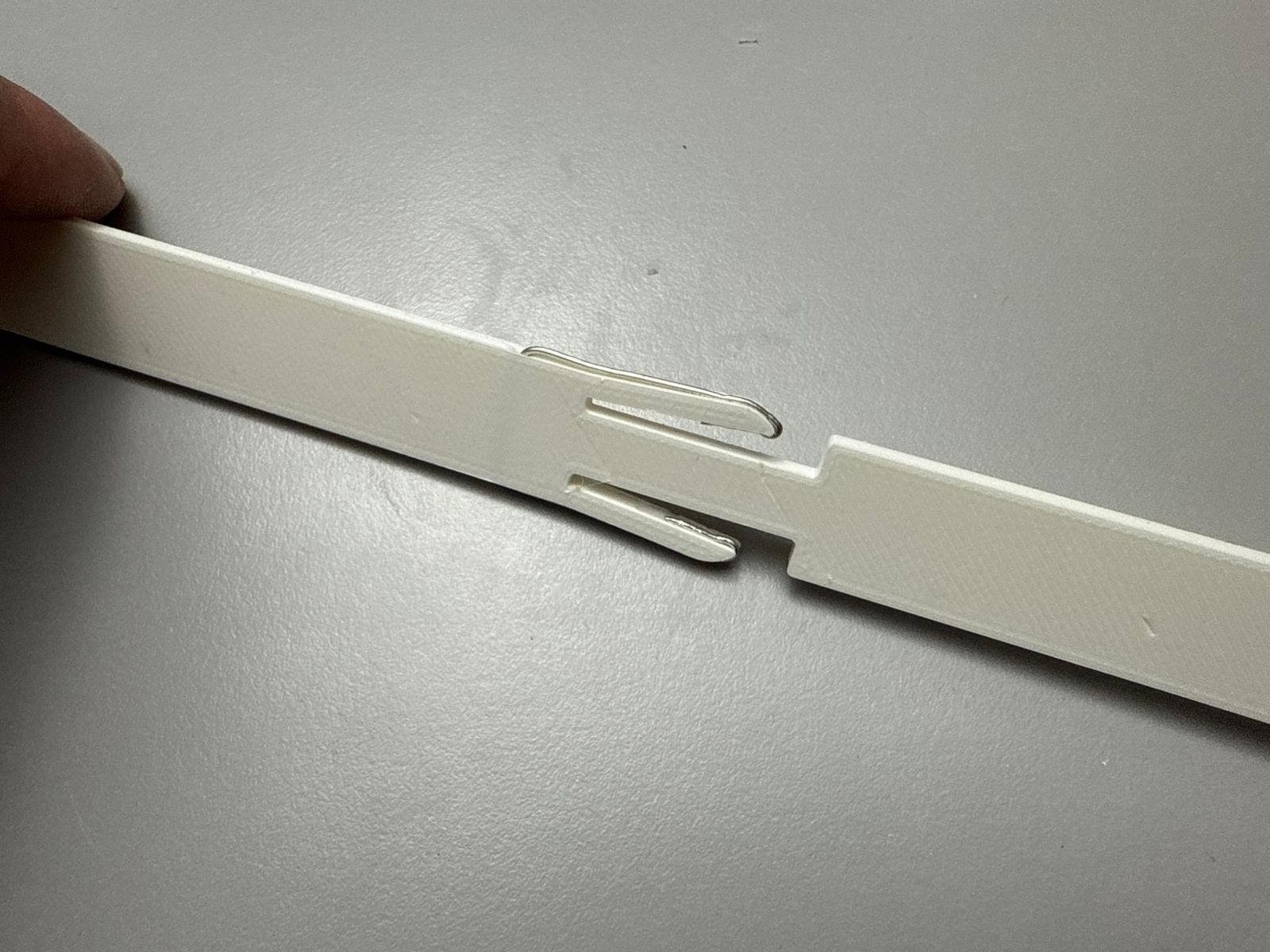
In conclusion I realized my first step is to redesign the tine itself and this was my *Material* Integration* as I struggled to find a way to embed a conductive
material inside the 3d printed tine. Below is a sequence of the tine development process from a standalone 3d printed tine to an integrated conductive tine
The outputs of my conceptual design acheived two outcomes, first I finalized my tine design to meet the criteria of being 3d printed,spring loaded and conductive.
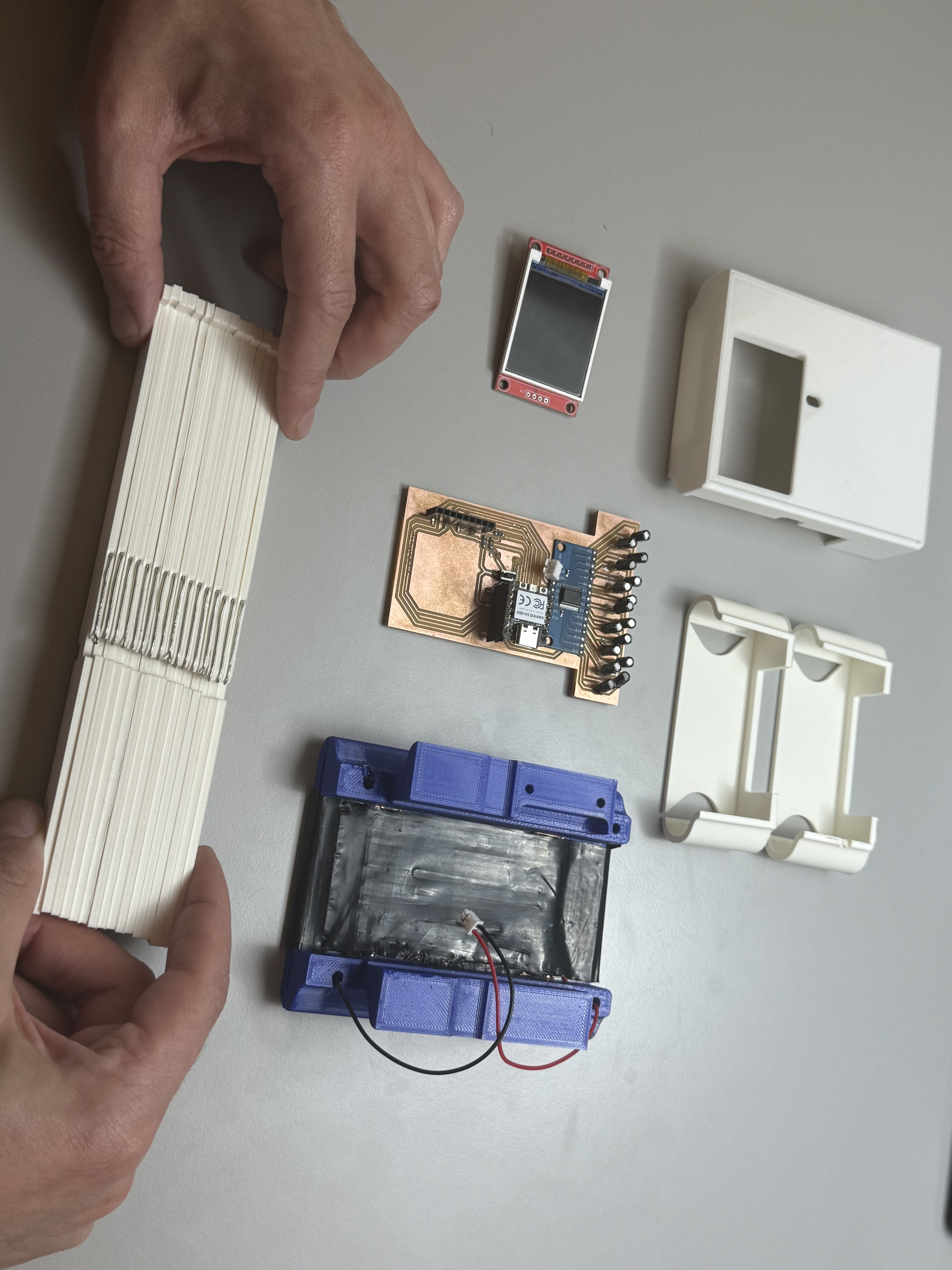
The second output as documented in my previous assignment weeks (8,9,10,11) I acheived a mature state of having a solid foundation for my electronic section.
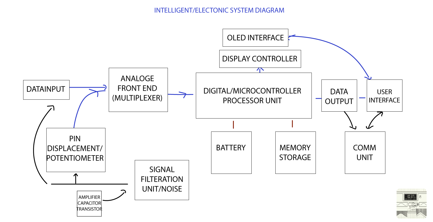
Regarding my electronics, I was following the following system integration diagram (also found on my final project documentation page
## Preliminary design
My preliminary design phase consisted of two parts , the first is the PCB module I intend to use and the second was modelling an enclosure around it
### Initial Preliminary 3D Model:
In the preliminary model, I was approaching my design to integrate the tines into fixed tracks and inspired by the instrucrable tutorial I refer in my final project, I was
considering a conductive filament track instead of velostat, however due to the unavailability and the high experimintational risk and cost, I stuck to velostat and adapted the design further.
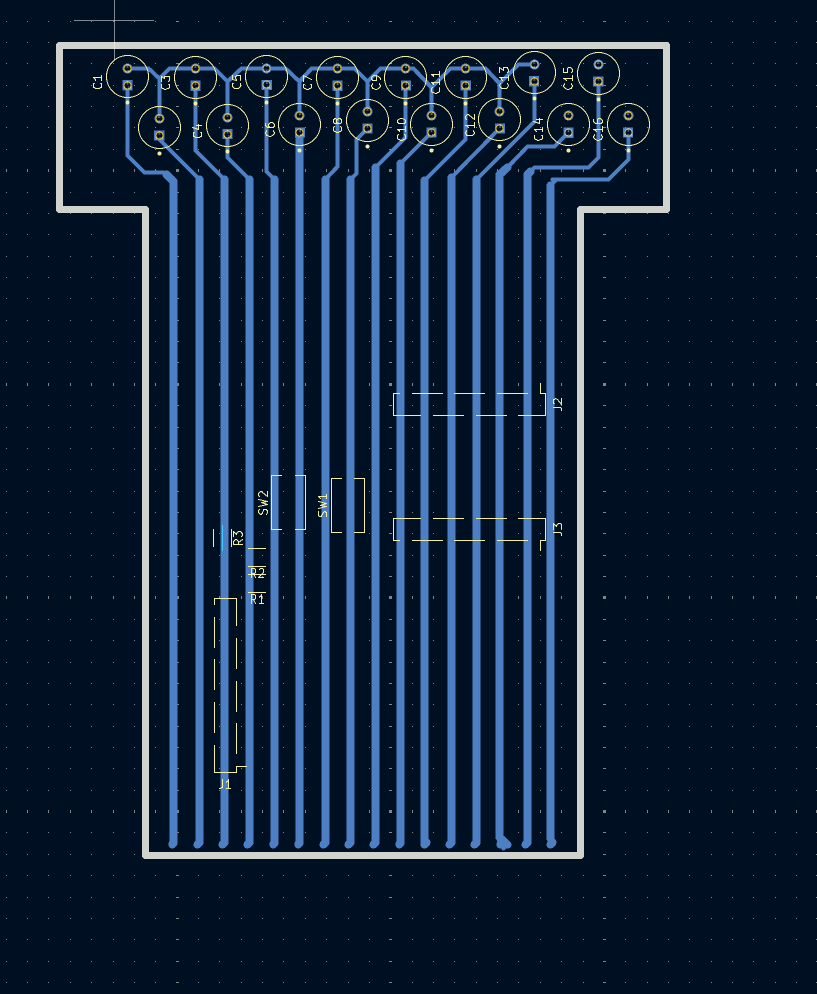
### KiCAD PCB preliminary design
My KiCAD journey for this was absolutely crazy. I started off by creating my schematic and components list, to which my struggle was to find enough space for all
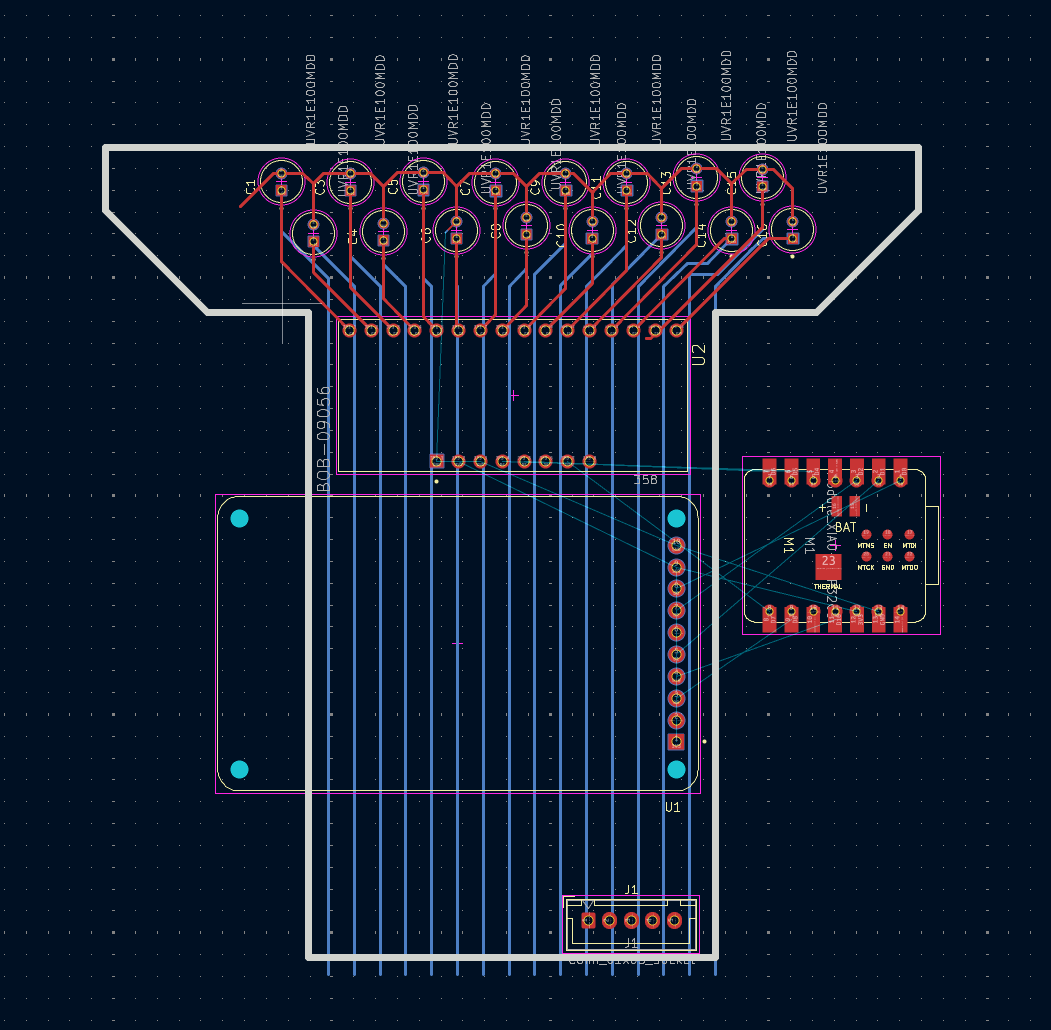
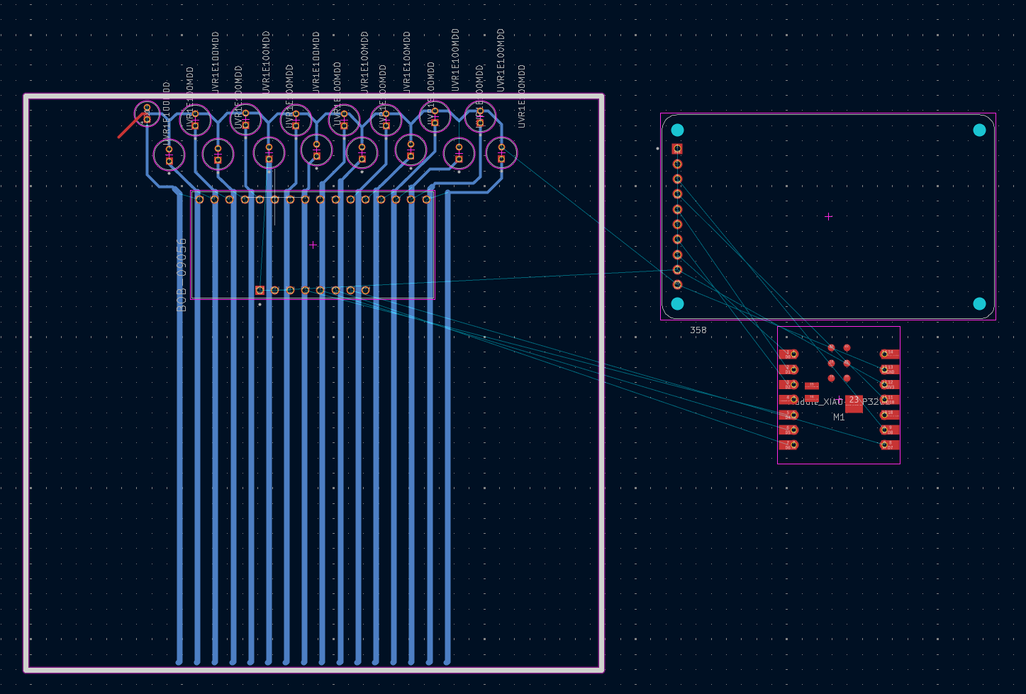
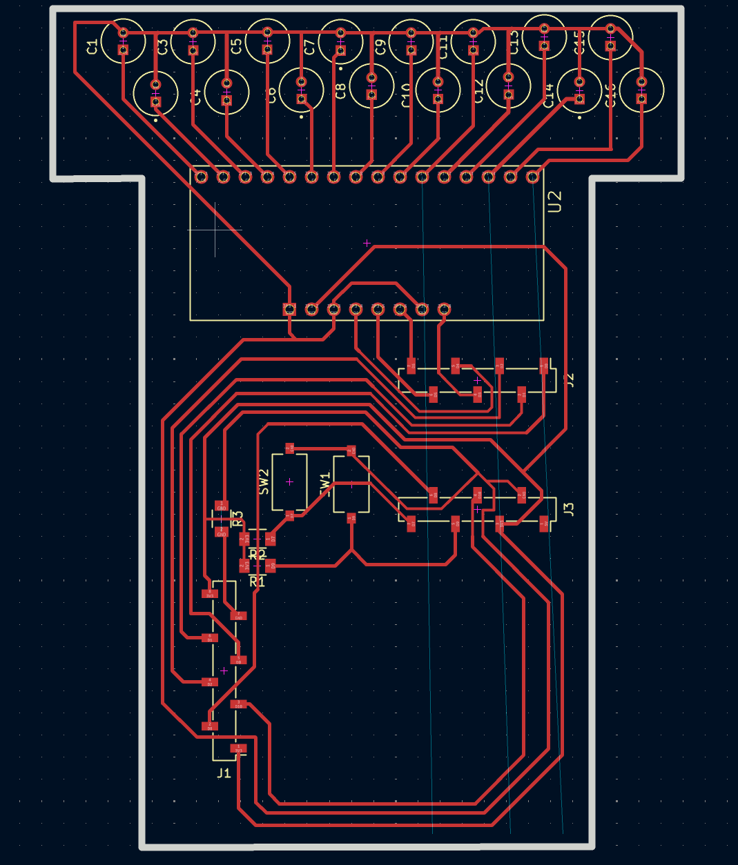
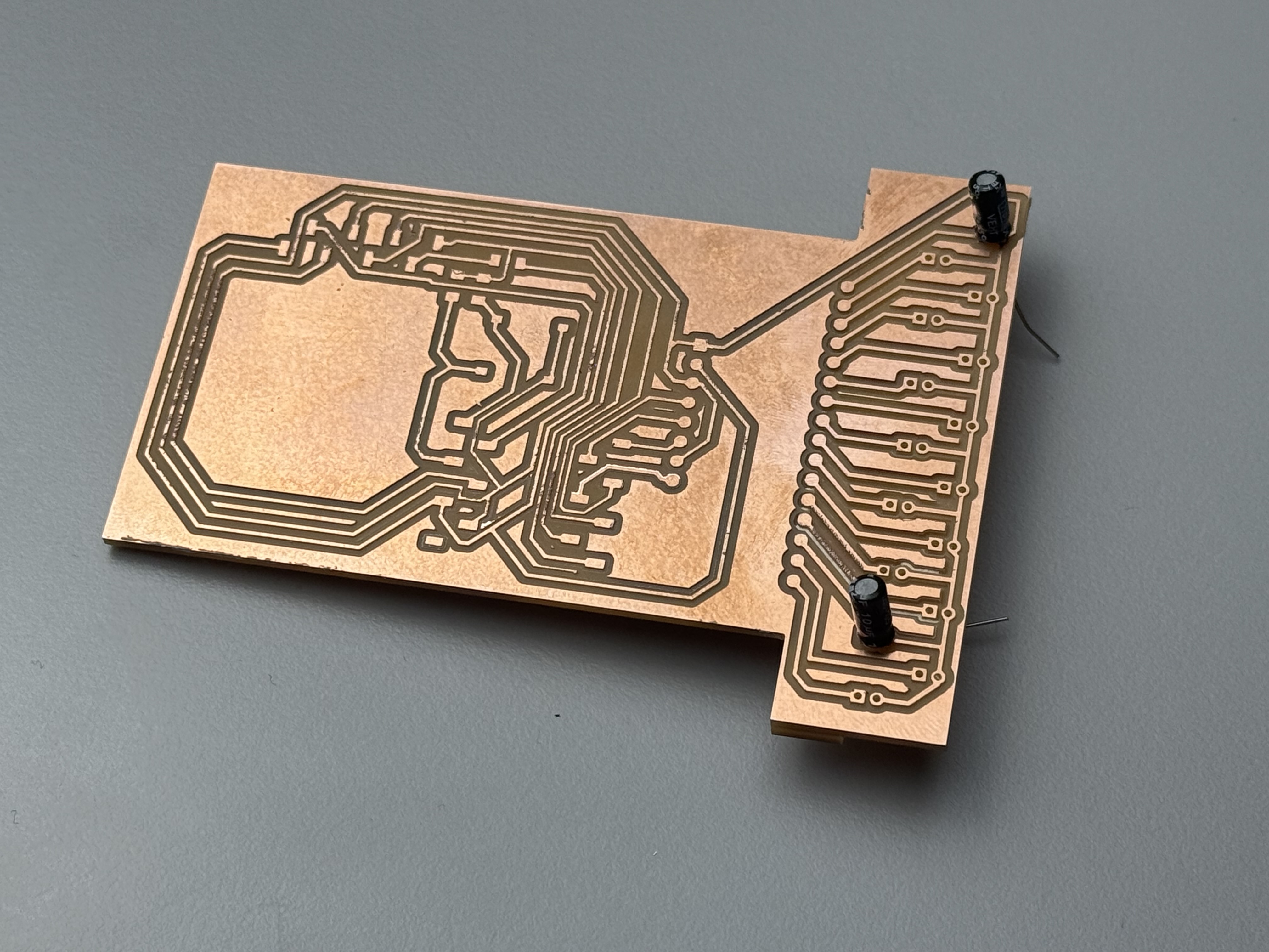
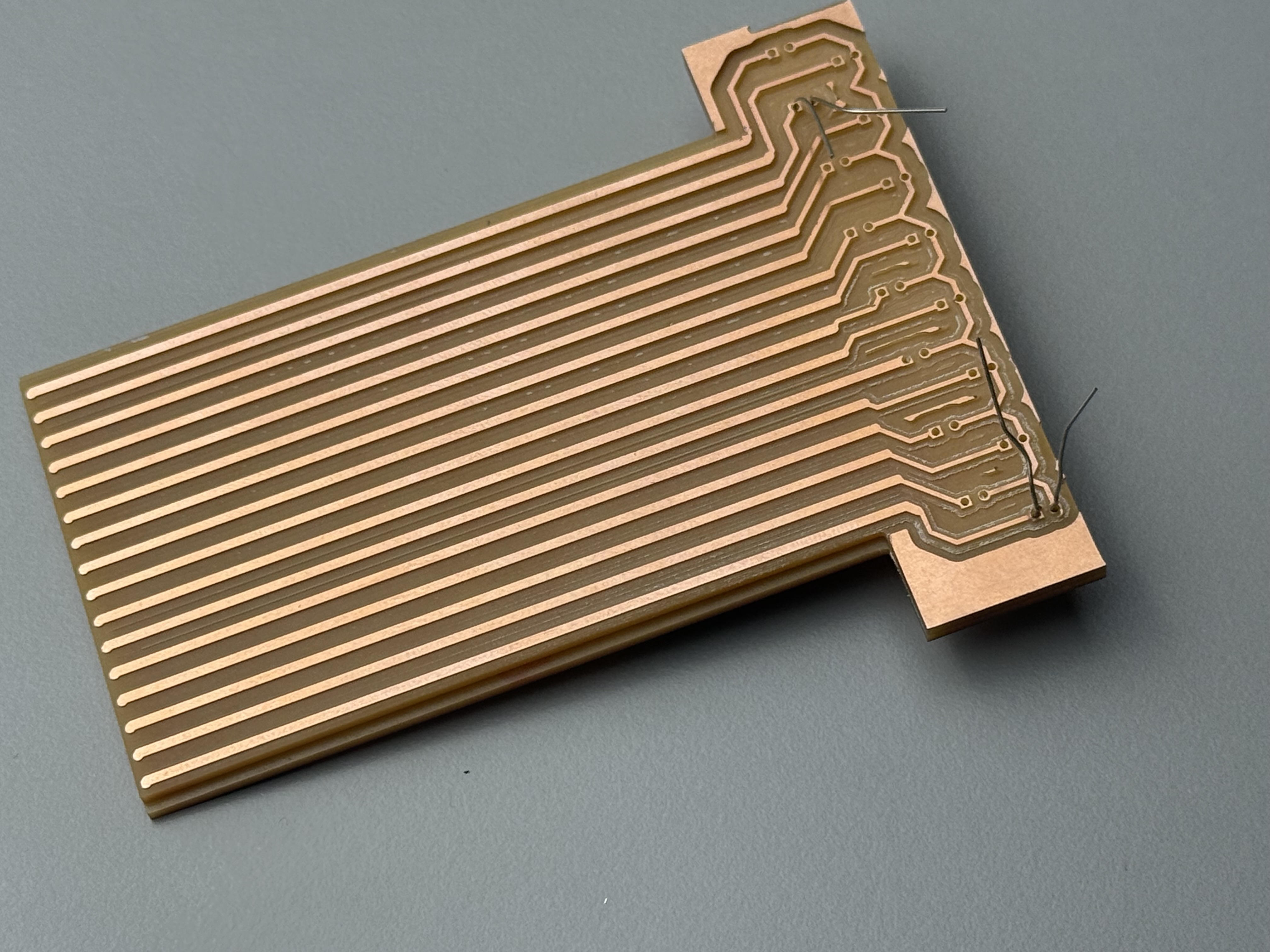
the traces. After numerous attempts to route the traces I ended up with the following results, integrating all the paths into a single double layered PCB
First Iteration
Second Iteration
Final Iteration - Front CU
Final Iteration-Back Cu
What I did here was I used the capacitor holes as *Vias* and alignemnts to the back copper layer
The front/top copper layer served as the central station for all the logic/back end wiring if you want to call it, and the back layer/bottom , was 16 straight
tines which will make contact with the tines.
## Detailed Design
I have been familiar to work with the design thinking approach in my experience so I followed through it , to summ it up:
Define : Transform the mechanical contour guage into a fully working intelligent and digital version
Ideate : Integrate slide motion along with a custom built potentiometer and CAD softwares to extract contour profiles
### Prototype Development Roadmap and Recap
The prototyping phase is summarized below, establishing targeted goals to evaluate different system modules:
| Cycle | Prototyping Objectives | Status / Scope |
| :--- | :--- | :--- |
| **Prototype 1** | Evaluate mechanical tolerances, structural integrity, hardness, and surface finish of 3D-printed chassis components. | **Completed** |
| **Prototype 2** | Test fundamental electronic hardware and map the initial design for a custom milled PCB integrating multiplexers and high-impedance potentiometer nodes. | **Completed** |
| **Prototype 3** | Formulate a physical Proof of Concept (POC) to test mechanical alignment and structural fitment between sliding tines and the central electronic assembly. | **Completed** |
| **Prototype 4** | Build and test Version 1 of the custom sensor array stackup to benchmark voltage distribution. | **Completed** |
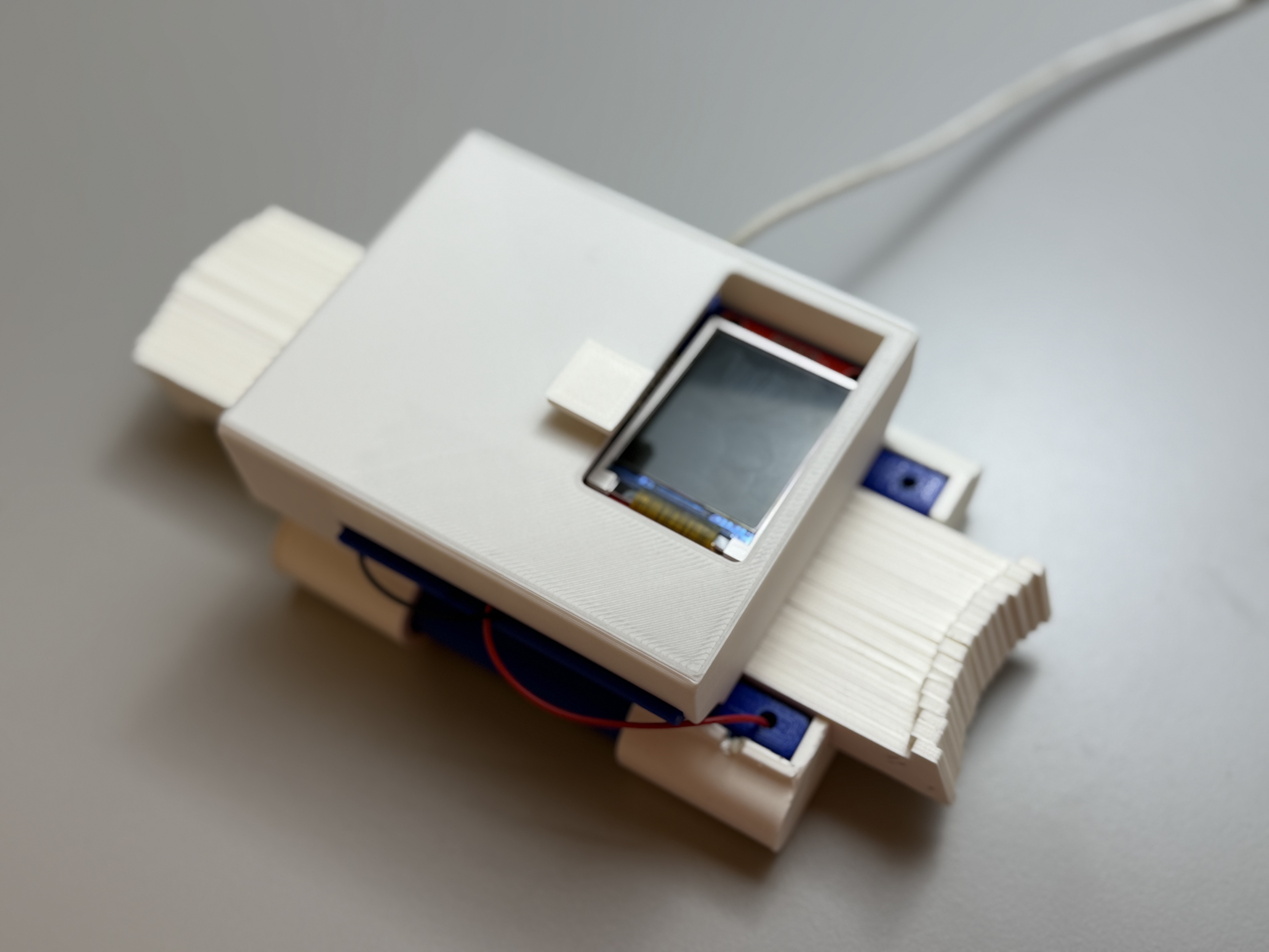
| **Prototype 5** | Establish a functional Proof of Concept for the localized user interface screen rendering and downstream hardware communication architecture. | **Completed** |
### Design Progression
* **Conceptual:** Making a Proof of Concept for the electronics part and the main assembly of the digital contour guage,integrating them into a simple mockup and a test canvas to iterate over for the preliminary design.
* **Preliminary:** The preliminary design is in the 3D modelling phase.
* **Detailed:** Detailed subassembly designs are stil in the CAD phase
This finally led me to my final design shape , to which it consisted of multiple components and sub assemblies which I will detail further in my final project page
This structural module runs on two distinct tracking substrate scenarios detailed in the grid layout below.
### Sub-Assembly Breakdown
* **Main Assembly:** The unified tool enclosure bringing together and securing the matching dual-sensor structural board stackup.
* **Sub-Assembly 2 (The Tine Array):** Tight-fit sliding pins tracking edge-to-edge, populated with low-friction steel roller bearings serving as local electrical bridge points.
* **Sub-Assembly 3 (Front Sensor & Logic Frame):** House frame containing multiplexers, interface guide walls, the OLED display, and the interface button.
* **Sub-Assembly 4 (Electronic Module Casing):** A custom protective cover preventing internal dirt or particulate contamination.
* **Sub-Assembly 5 (The Dual-PCB Substrate):** Milled single-sided copper FR1 laminates designed explicitly to align face-to-face and complement each other to close the tracking loop.
## Packaging & Spatial Packaging
### Fasteners & Alignment Mechanics
* **Standoff Elimination:** Traditional nylon standoffs are to be completely replaced by tight sliding channel tracks integrated directly within the internal perimeter walls of the plastic enclosure shell.
* **Wire Routing & Fatigue Elimination:** **Zero moving internal wiring.** All sensor signals bridge directly via physical steel rolling contacts running on stationary tracks.
* **Tine Alignment:** The pins are positioned closely next to each other. By filling the fixed housing width perfectly, the elements apply natural sideways compression against one another to clear alignment play. When using *Conductive Filament*, the printed paths natively double as integrated tracking rails.
### Tactile Surface Finish
Surface resolution parameters are dictated strictly by FDM manufacturing constraints. Friction performance and sliding coefficients are explicitly tuned using calculated layer heights ($0.2\text{mm}$) and specific nozzle geometries ($0.4\text{mm}$).
## Testing, Diagnostics & Failure Analysis
### Quality Protocols
* **QA (Defect Prevention):** Enforced electronic clearance boundaries inside the KiCAD layout file and oversampling software routines to eliminate noise harmonics.
* **QC (Defect Detection):** Hardware multi-point terminal checks with a digital multimeter paired with sequential software diagnostic script checks.
### Stress Bounds & Mitigation Strategy (FMEA)
* **Elastic Over-Extension:** An internal structural end-stop lip blocks tines from slipping completely out of the frame.
* **Stress Splitting:** 0.3-1.5mm internal structural fillets sweep away sharp high-stress corner junctions.
* **Fastener Backout:** Thread-locking Loctite 242 secures all primary mechanical fastening locations.
* **Thread Stripping:** Brass inserts directly screwed into structural plastic (PLA).
* **Slide Jamming:** A 0.1mm physical spacing gap is maintained between sliding faces to protect against thermal expansion.
* **Floating Gates:** 10kOhm inline pull-down resistors ground the multiplexer signal lines when a roller breaks contact.
## Microcontroller Scalability Matrix
The board is designed for high drop-in compatibility across RP2040 AND ESP32C3 microcontrollers sharing a standard structural packaging footprint:
| Hardware Parameter | Seeed Studio XIAO ESP32C3 | Seeed Studio XIAO RP2040 |
|:---|:---|:---|
| **Processor Core** | Single-Core 32-bit RISC-V Architecture | Dual-Core 32-bit ARM Cortex-M0+ Core |
| **ADC Bit-Depth** | 12-bit Resolution ($0-4095$ bounds) | 12-bit Resolution ($0-4095$ bounds) |
| **Analog Noise Jitter** | Higher internal noise variance | Clean, lower baseline analog curves |
| **Firmware Overhead** | Demands aggressive digital software filtering | Operates on light data averaging loops |
| **Core Configuration** | Single I2C channel optimization | Configurable Programmable I/O blocks (PIO) |
### Pro-Repair & Circular Lifecycle
The tool utilizes standard M2 hardware fasteners throughout. Worn-down individual 3D-printed tines can be swapped out independently without disturbing the underlying sensor electronics or dual-PCB core architecture.