Group Assignment: Signal Testing
## Group Assignment
- Use the test equipment in your lab to observe the operation of a microcontroller circuit board (as a minimum, you should demonstrate the use of a logic analyzer)
- Document your work on the group work page and reflect what you learned on your individual page
Full group documentation can be found on our **[Lab Group Page](https://fabacademy.org/2026/labs/techworks/week6/week6.html)**.
## Overview
This week focused on **PCB design** and preparing a board for manufacturing.
The objective was to design a functional PCB and understand the complete workflow from:
> Idea → Schematic → PCB Layout → Manufacturing Preparation
### Core Concepts & Definitions
| Term | Definition |
| --------------------------------- | ------------------------------------------------------------------------------------------ |
| **PCB** | Board that mechanically supports and electrically connects components using copper traces. |
| **Schematic** | Logical electrical diagram showing components and their connections. |
| **Symbol** | Graphical representation of a component in the schematic. |
| **Footprint** | Physical pad layout of a component on the PCB. |
| **Package (Size)** | Physical dimensions/type of a component (e.g., 0603, QFN, DIP). |
| **Pin Pitch** | Distance between the centers of two adjacent pins. |
| **SMD** | Surface Mount Device – mounted directly on PCB surface. |
| **THT (Through-Hole Technology)** | Components inserted through drilled holes and soldered on the opposite side. |
| **Net** | Electrical connection between two or more pins in the schematic. |
| **Label** | Used to name signals instead of drawing long wires. |
| **Minimum Clearance** | Minimum spacing allowed between copper elements. |
| **Minimum Track Width** | Smallest allowed width of a copper trace. |
| **Multilayer PCB** | PCB with more than two copper layers for complex routing. |
| **Milling** | Mechanical removal of copper using a CNC machine. |
| **Etching** | Chemical removal of unwanted copper. |
| **Silkscreen** | Printed top layer used for labels, orientation marks, and logos. |
| **Design Rule Checker (DRC)** | Tool that checks PCB against manufacturing constraints. |
| **Warning (KiCAD)** | Issue that may function but requires review. |
| **Error (KiCAD)** | Issue that must be corrected before manufacturing. |
| **Thick Traces** | Used for high-voltage or high-current lines to reduce resistance and overheating. |
As part of my **Final Project** I decided to explore designing a PCB which will function with my **Digital Contour Profiler**.
The concepts I am hoping to successfully apply is designing a PCB with a multiplexer connected to an OLED screen.
| Category | Component Name | Key Specifications | Link / Reference |
| :--- | :--- | :--- | :--- |
| **Microcontroller** | Raspberry Pi RP2040 | Dual-core ARM Cortex M0+ | [Base Chip] |
| **Microcontroller** | ESP32 Series | Wi-Fi & Bluetooth MCU | [Base Chip] |
| **Display** | 0.96" OLED Module (White) | 128x64 Resolution, I2C (4-Pin) | [View Product](https://mikroelectron.com/product/me-6857) |
| **Display** | 0.96" OLED Module (Blue) | 128x64 Resolution, I2C (4-Pin) | [View Product](https://mikroelectron.com/product/me-707) |
| **Display** | 0.96" OLED Module (Blue) | 128x64 Resolution, SPI (7-Pin) | [View Product](https://mikroelectron.com/product/me-6865) |
| **Logic IC** | SN74LS153N Multiplexer | Dual 4-to-1 Data Selector | [View Product](https://mikroelectron.com/product/me-6678) |
| **Logic IC** | CD74HC4067 Breakout | 16-Channel Analog/Digital MUX | [View Product](https://mikroelectron.com/product/me-2912) |
## Applying Multiplexing
It took me sometime to grasp the idea of multiplexing,in concept its simple.
A microcontroller such as the **ESP32C3** has a defined number of pins , the challenge I was addressing
is that the ESP32C3 has only **four analoge** pins (D0,D1,D2,D3) and I will need ..more.
So after alot of questions and answers and googling, I would say a multiplexer is basically (in mechanical terms) a manifold.
It means I can utilize a single analoge pin and branch it out to receive more inputs/outputs.
But its more complex internally, to acheive that the pin needs to be able to read/write and communicate with this multiplexer/manifold.
To understand it completely I had to familiarize myself with the following concepts:
**Enabler pin (EN)**: This is the "Master Valve." It is an Active Low pin, meaning it must be connected to GND to allow the signal to flow. If it is pulled HIGH, the manifold is "locked," and no communication happens.
I learned that it is smart to keep it GND saving one more pin on the ESP32C3
I also learned this is all acheived through a communication path; to cut it short, here's a table explaining how to connect ESP32C3 to CD74HC4067 multiplexer:
| ESP32C3 Pin | CD74HC4067 Pin | Explanation |
| :--- | :--- | :--- |
| **D0** | **SIG (Common)** | The "Mouth" of the manifold. Connected to D0 (ADC1) to ensure stable analog readings even when Wi-Fi is active. |
| **D1, D2, D3, D10** | **S0, S1, S2, S3** | **Address Pins:** These 4 digital pins use binary logic to select which of the 16 channels is connected to D0. |
| **GND** | **EN (Enable)** | **The Gatekeeper:** Since this pin is "Active Low," we tie it to GND to keep the MUX "Always On" and save a GPIO pin. |
| **3V3** | **VCC** | Power supply for the multiplexer's internal switching logic. |
| **GND** | **GND** | Common ground reference to ensure a consistent 0V baseline for all sensors. |
Why D0 and not D5?
While the ESP32-C3 can technically read analog signals on D5, it is part of ADC2, which often becomes noisy or stops working when Wi-Fi is active. By using D0 (ADC1), your sensor readings remain stable. Additionally, using D0 keeps D4 and D5 free for I2C communication, allowing you to add an OLED display or extra sensors later without a hardware conflict.
In digital logic, HIGH and LOW are the "On" and "Off" states of your manifold's control system.HIGH ($3.3V$): Sending a HIGH signal to an Address pin (S0-S3) flips an internal switch.LOW (0V-GND): Sending a LOW signal to the EN pin "unlocks" the chip so it can function.
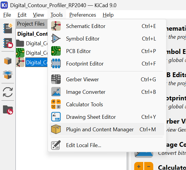
## Working with KiCAD
KiCAD has become one of my "frequently" used softwares. I learned how to use libraries, footprints, plugins, and some tips and tricks which I will cover.
### Step 1: Downloading KiCAD
KiCAD can be downloaded from the official website [Kicad.org](https://www.kicad.org/download/). The installation process is pretty straightforward.
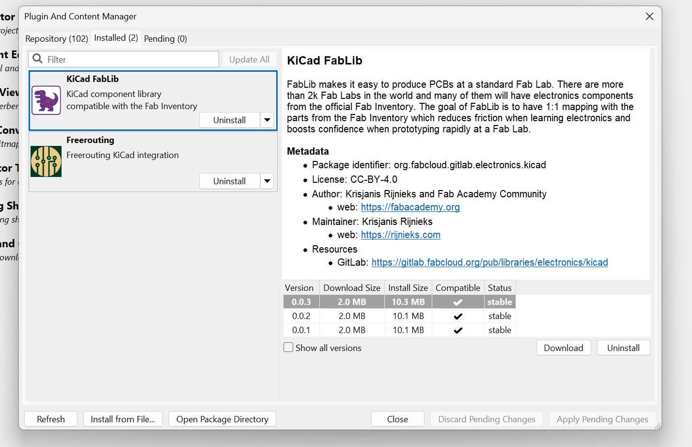
### Step 2: Discovering Plugins
I installed **KiCAD Fablib**, which is a great resource for symbols and footprints for almost all electronic components within FabAcademy. I also was curious to find if there was a different way to "manually" draw the traces, which led me to the **Freerouting** plugin.
### Step 3: Applying Concepts
The first thing to know about KiCAD is that it has a Schematic Editor and a PCB Editor. A standard project contains a `.kicad_sch` file and a `.kicad_pcb` file. As the name suggests, one is for drawing the schematic (using symbols) and the other is for modeling the PCB (using footprints).
### Step 4: Designing a PCB
It's important to start with the schematic design, where I used labels, symbols, and attached footprints to different components, occasionally outsourcing those I could not find.
#### Shortcuts and Functions:
| Shortcut | Description | Where to use |
| :--- | :--- | :--- |
| **A** | Loads symbols and allows you to choose one | Schematic |
| **Ctrl + L** | Create Global labels to insert into components | Schematic |
| **M** | Move objects around | Schematic + PCB |
| **N** | Adjust Grid spacing | PCB |
| **X** | Draw a Trace | PCB |
| **Alt + 3** | Open 3D Viewer | PCB |
| **X/Y* | Front/Right Views in 3D space | 3D Space |
| **ctrl+shift+l* |Draw Lines | PCB|
Other functions I worked with:
- **Selection Filter:** This really helped me iterate my traces; by checking only "Tracks," I could quickly select all and start over.
- **Shape Modification:** By selecting a shape on the PCB layout, you can modify it (e.g., adding fillets).
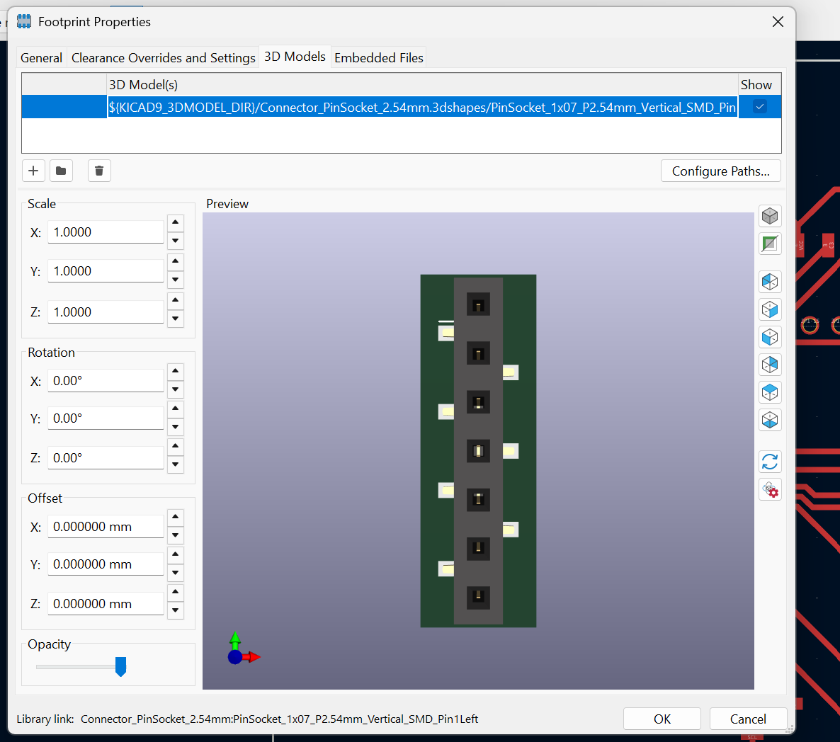
- **3D Models:** Double-clicking a footprint lets you access the assigned 3D shape and adjust its position, height, or file source.
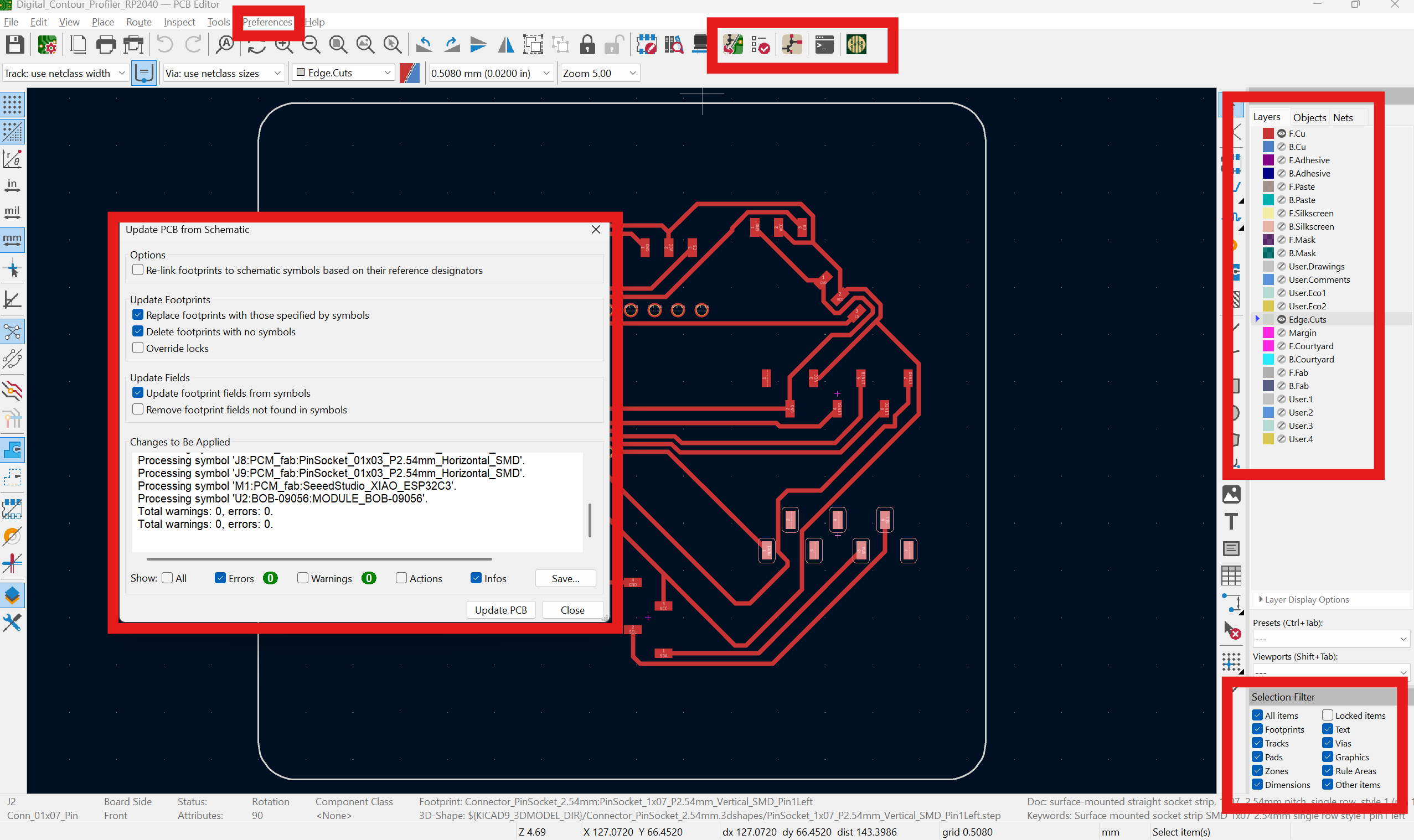
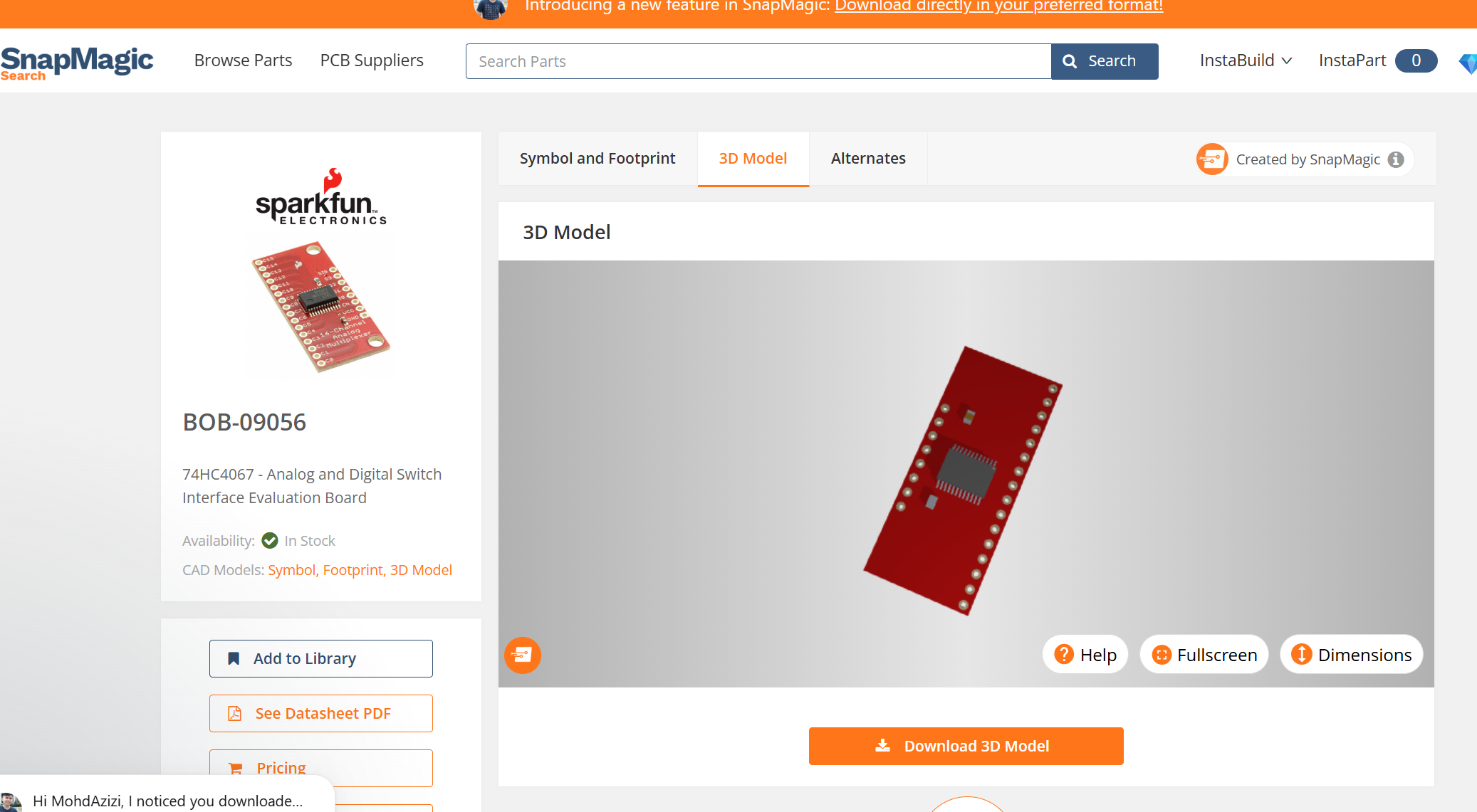
- **Manage Footprint/Symbol Library:** Found under Preferences; I used this to add libraries downloaded from [SnapEDA](https://www.snapeda.com/parts/BOB-09056/SparkFun/view-part/).
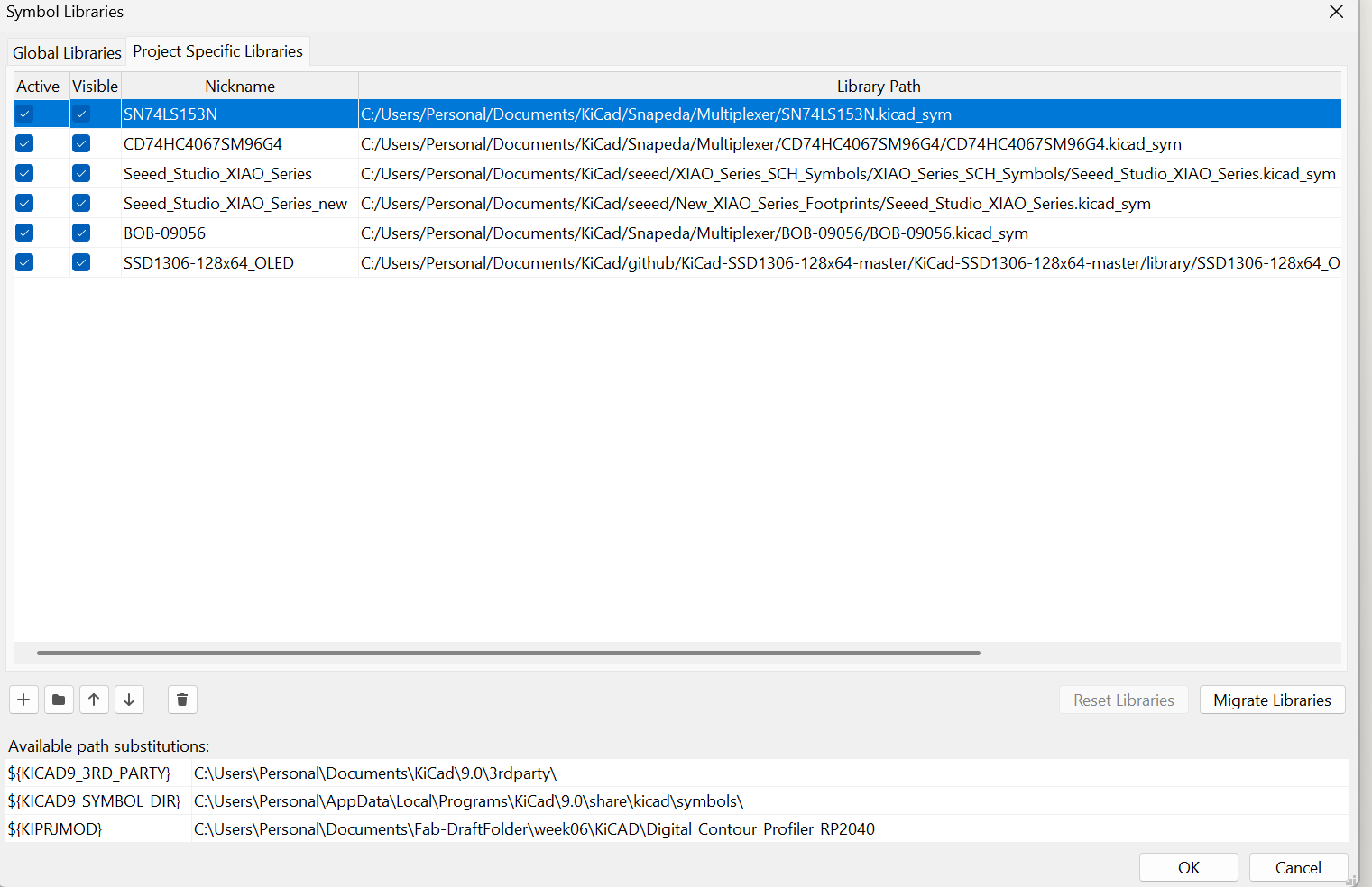
- **Project Specific Libraries:** This allowed me to filter exactly what I needed and update specific footprints/symbols without affecting global settings.
- **Board Setup and Constraints:** This is where we defined the track widths and clearances.
- **Net Classes:** Associated with the Freerouting plugin; defining parameters like clearance and track width here reflects in the Freerouting settings.
- **Footprint Properties:** Double-clicking a footprint in the PCB layout allows you to adjust X/Y coordinates and rotation angles.
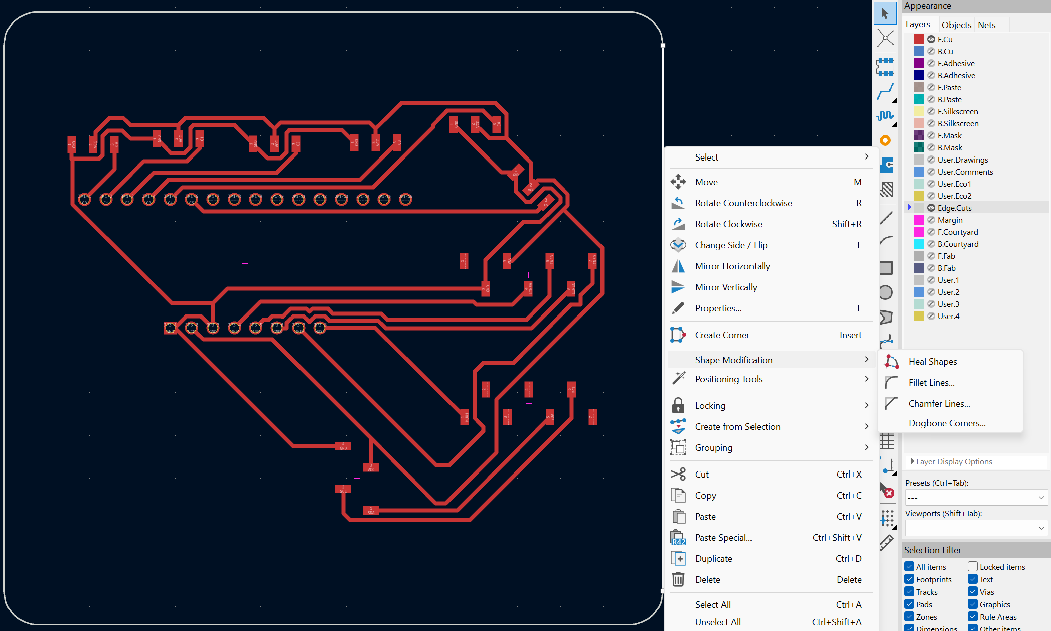
Shape Modification - Fillet
3D Models Tab
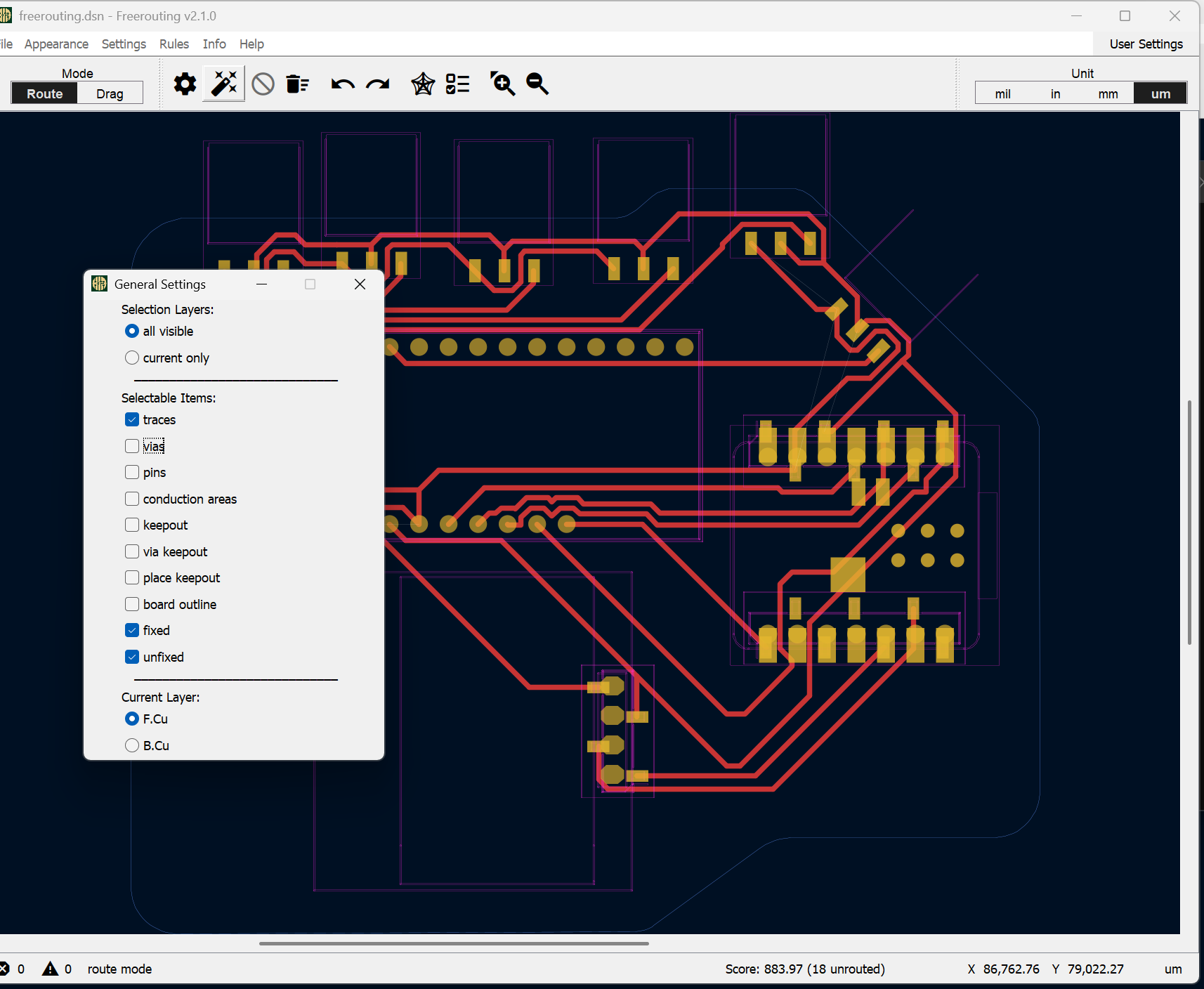
General Overview (UI Elements)
Downloading from Snapeda
Using Project Specific Libraries
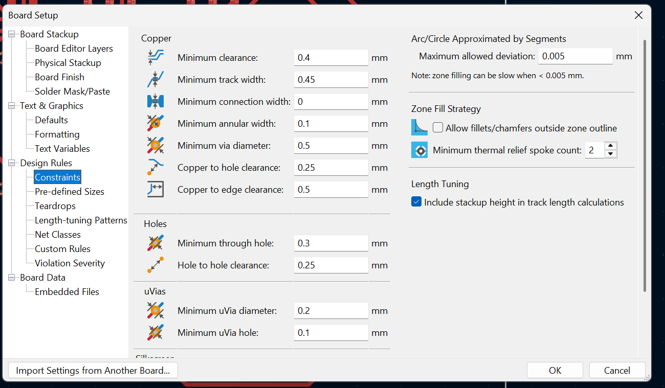
Applying Constraints
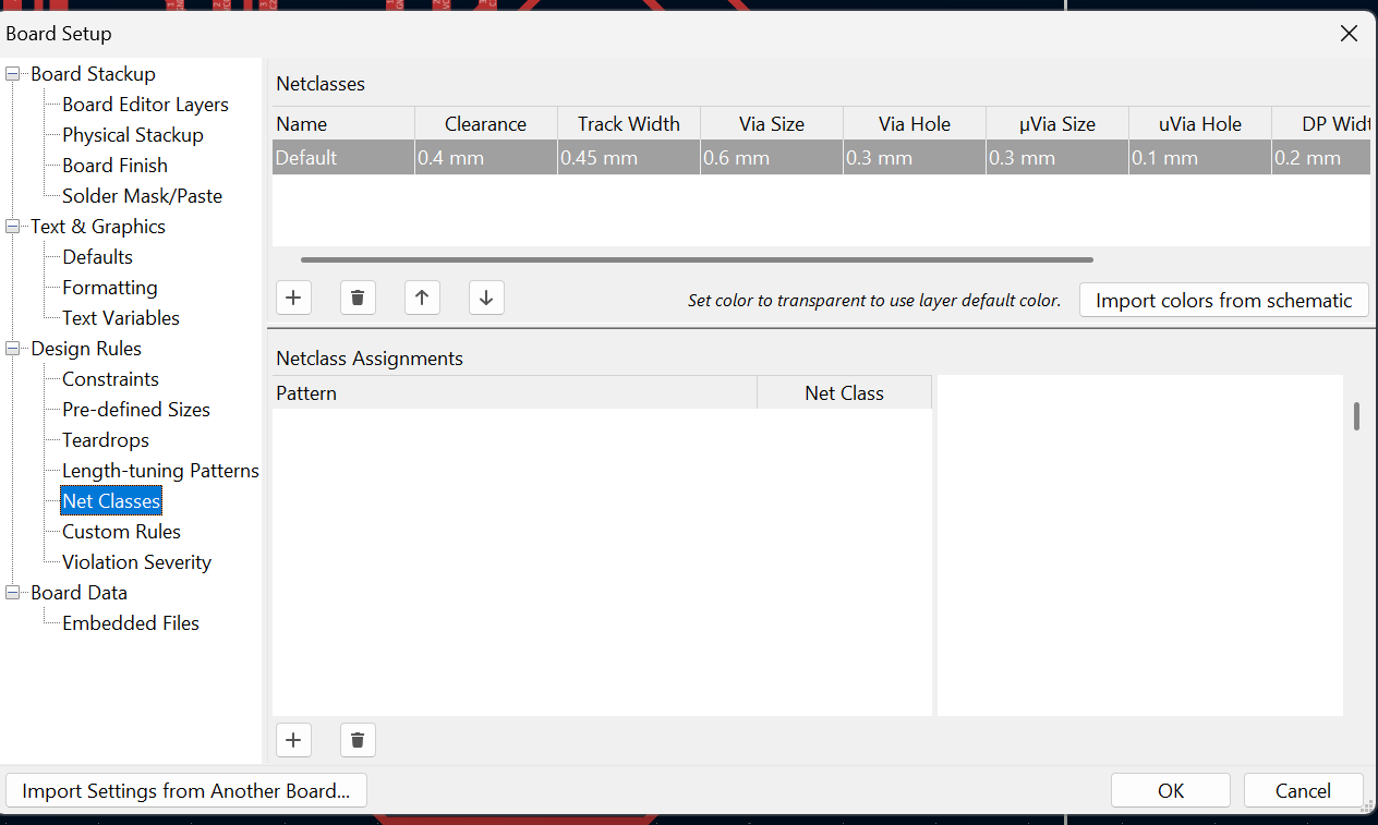
Using Netclasses
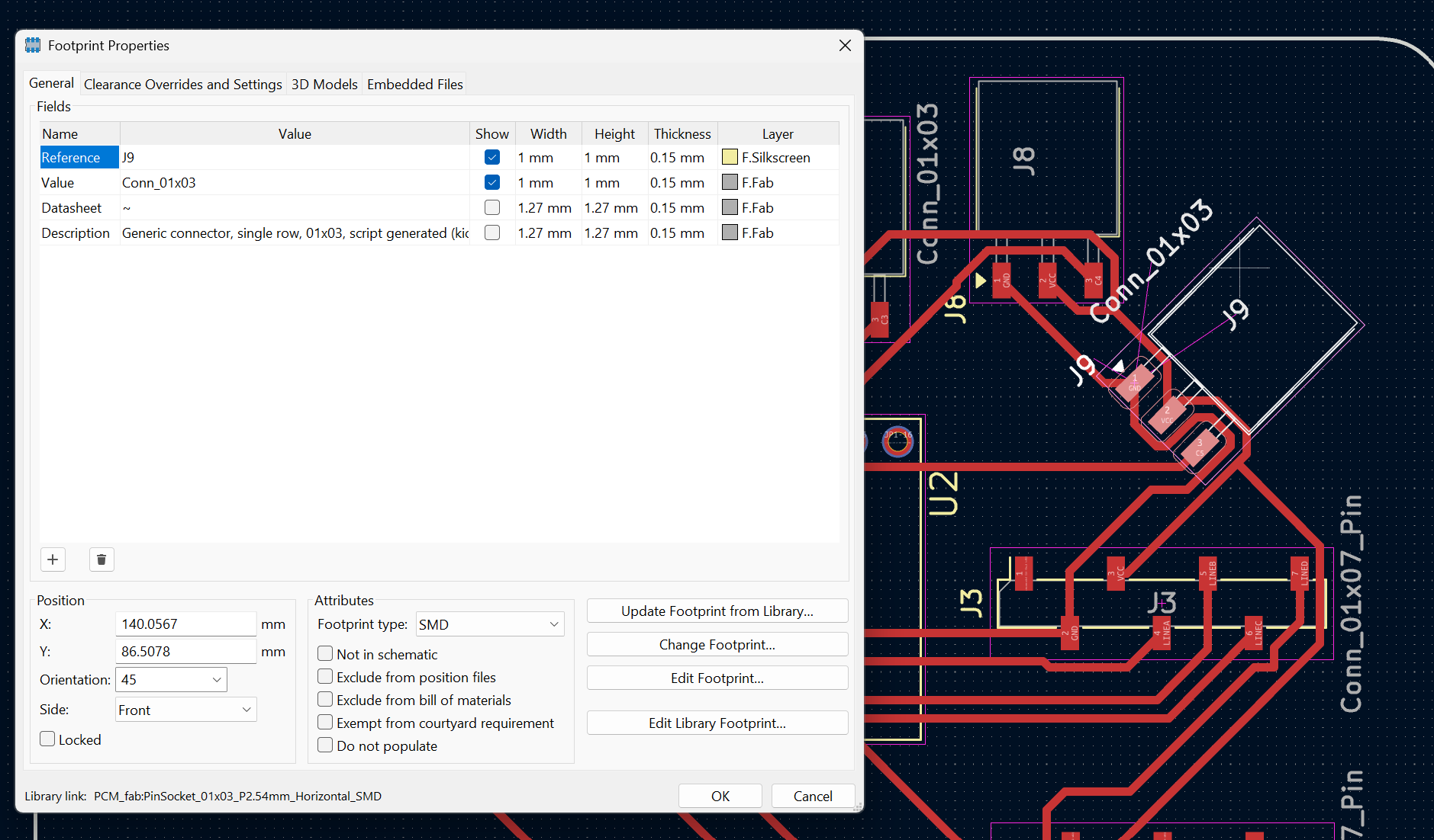
Footprint Properties
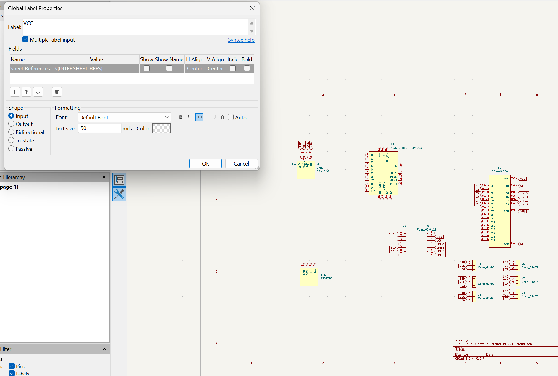
Adding Labels in Schematic
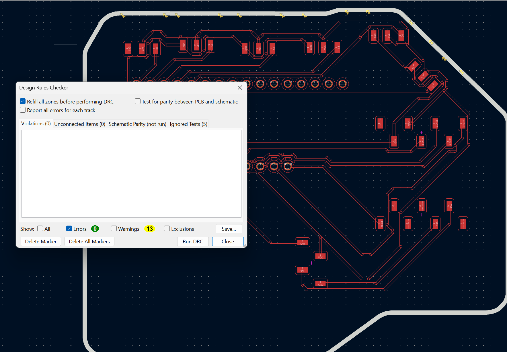
Always run DRC prior to exporting the files from KiCAD, mainly addressing any errors found
## Using Freerouting Plugin
I am not the best at drawing or manual sketching, and that is where **Freerouting** came into the picture. The Freerouting plugin can be directly downloaded from the KiCAD plugin library. Here is the workflow I followed:
- **Step 1:** I prepared my schematic using labels, ensuring all connections were logically correct.
- **Step 2:** After some trial and error with track widths, I set my **Netclasses** to the desired constraints to ensure the plugin respected my design rules.
- **Step 3:** Since we are working on a **single-layer PCB**, I disabled the Vias and Back layer options in the routing settings.
- **Step 4:** I ran multiple iterations until I was satisfied with the overall layout and routing efficiency.
Not everything is automated—here is how to maximize the tool:
- The plugin does not always route 100% of the nets; it can sometimes hit an impasse.
- You can adjust the allowed trace angles (e.g., 45° or 90°) in the routing settings.
- Manual routing and component relocation were inevitable in my case to achieve a fully routed board.
General Settings - Freerouting
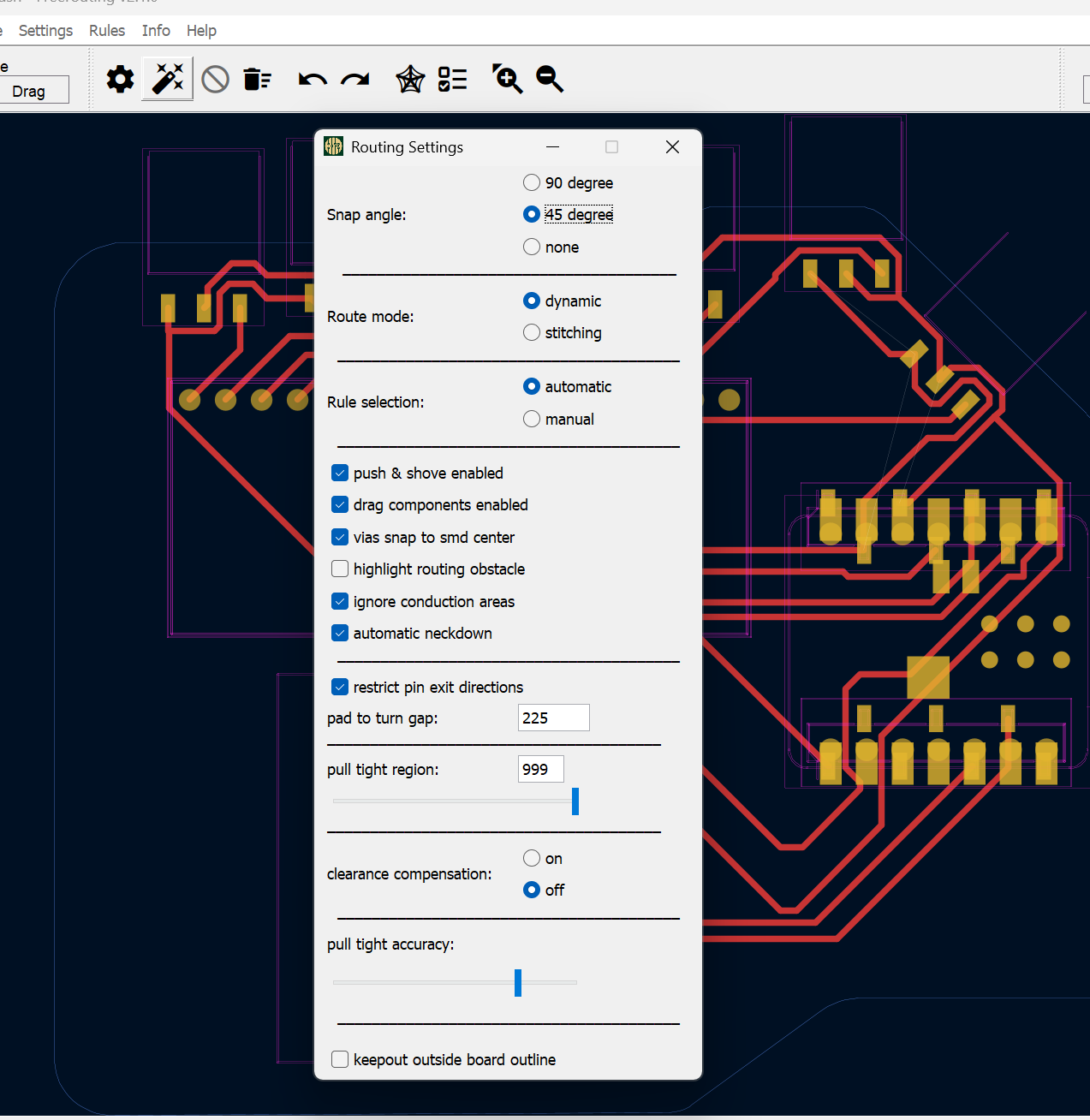
Routing Settings - Freerouting
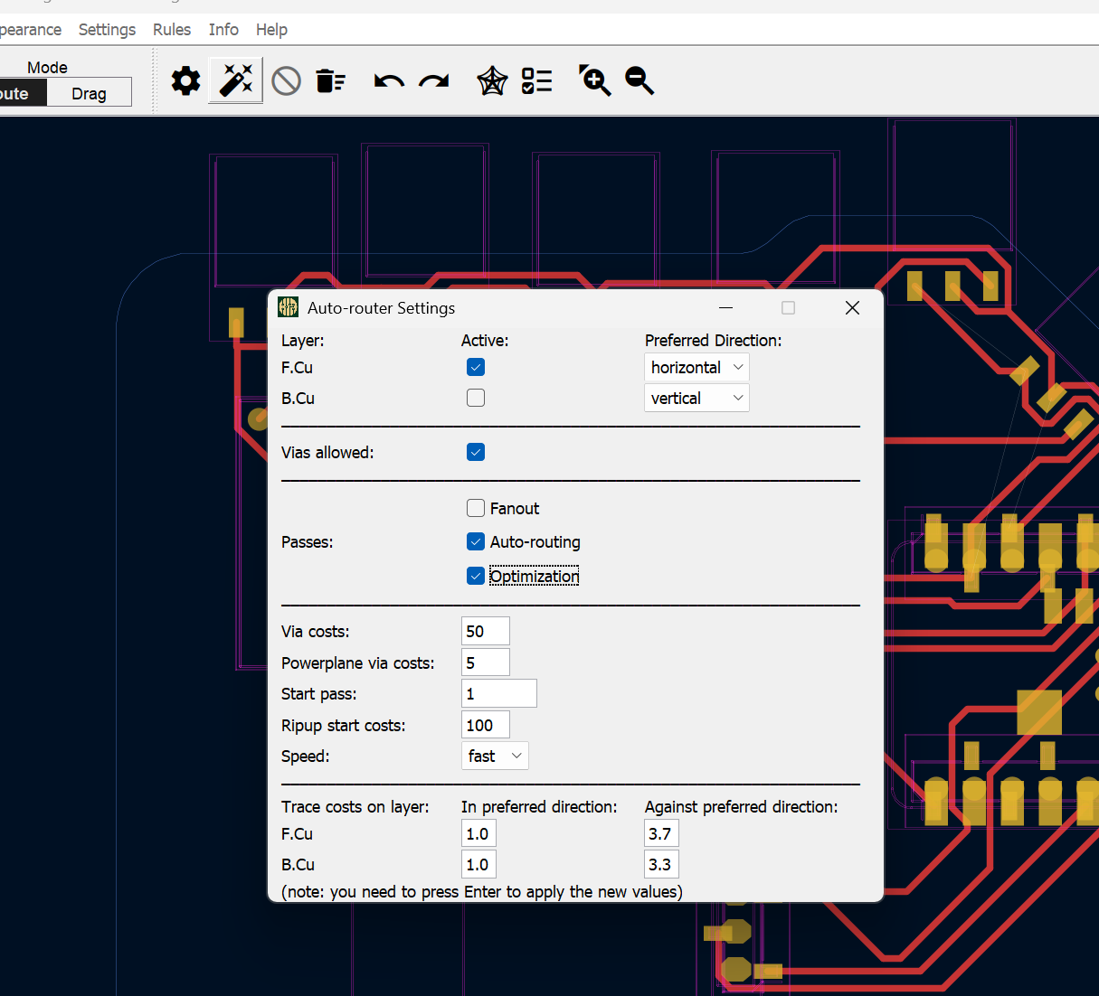
Auto-Routing Settings - Freerouting
## Individual Assignment
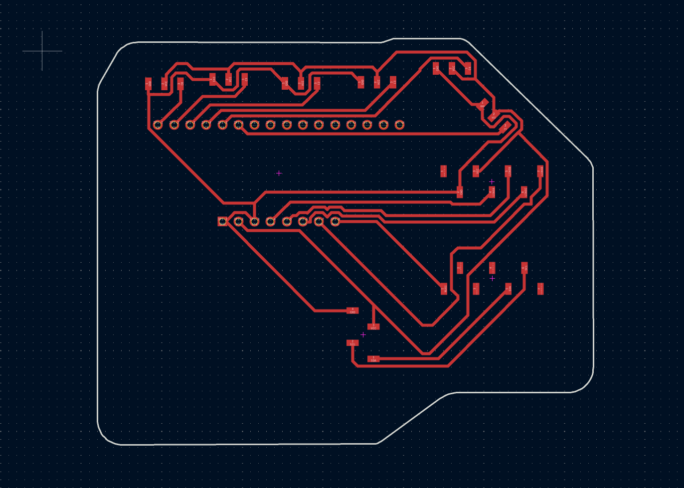
As mentioned earlier, my goal was to create a Proof of Concept testing PCB for my final project.
What I designed was a PCB which is split into experiments:
| Experiment | Goal | Expected Result |
| :--- | :--- | :--- |
| Socketed PCB | To use headers and map them with their corresponding components,to allow me to test different components in the future |Use the 4pin sockets to test different inputs starting with a potentiometer|
| Soldered Components | the Multiplexer is the keycomponent and I do not plan to change it (for now) so I decided to keep it soldered and to test my solder skills | implementing a THT assembly when I manufacture the PCB|
| No capacitors PCB | Im hoping to test the impact of different capacitors (Externally) for now to see how it would impact my analog signals and hopefully draft a resolution base for my final project | Noise and deviations |
### Final Steps: Plotting/Exporting to SVG
Using KiCAD Version 9.0, to export to SVG the option can be found in File>Plot>SVG
Here are the final results of my PCB design:
Plot to SVG
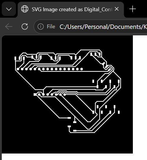
F.Cu SVG File
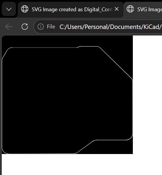
Edge SVG File
Reflow Soldering Process
## What I Learned: Reflow Soldering
Reflow soldering is the process we use for surface-mount electronics, and it’s basically like "baking" a circuit board. Instead of tackling one pin at a time with a hot iron, you prep the whole board and melt everything at once. It sounds complicated, but it really boils down to how you handle the solder and the heat.
The first step is applying **solder paste**, which is a thick, gray cream made of tiny metal beads and flux. To get it exactly where it needs to go, we use a **stencil**—basically a thin "mask" with laser-cut holes that match the PCB pads. You lay the stencil over the board, squeegee the paste across, and lift it to find perfect little piles of paste left behind. Because the paste is sticky, it acts like a temporary glue to hold components like my ESP32 and multiplexer in place so they don't slide around.
Once the parts are sitting on the board, the whole thing goes into a reflow oven or onto a hot plate. As it heats up to about 217°C, you can actually see the gray paste "reflow"—it suddenly turns into shiny, liquid silver. One of the coolest things I noticed is that surface tension helps pull the components into perfect alignment on the pads. Once it cools, you’re left with professional, solid joints across the entire board in one shot. It’s way faster than hand-soldering and much more reliable for the tiny parts I’m using in my projects.