Week 11: New PCB Documentation
Designing and fabricating a custom output visualizer and transmitter board with potential integration into the final project.
1. PCB Overview
After my initial PCB from Week 6 was unexpectedly damaged, I needed to design a replacement board. I used this opportunity to align the design with my upcoming final project needs—either as a remote controller device for the Digital Contour Gauge or a standalone wearable watch node.
For Week 11, this custom PCB was optimized primarily to function as an output visualizer and data transmitter. While the integrated input header suffered some damage during testing, the trace routing and core processing pipelines remained intact for system verification.
2. Design & Schematics
System Schematic
Board Layout
3. Milling & Assembly Steps
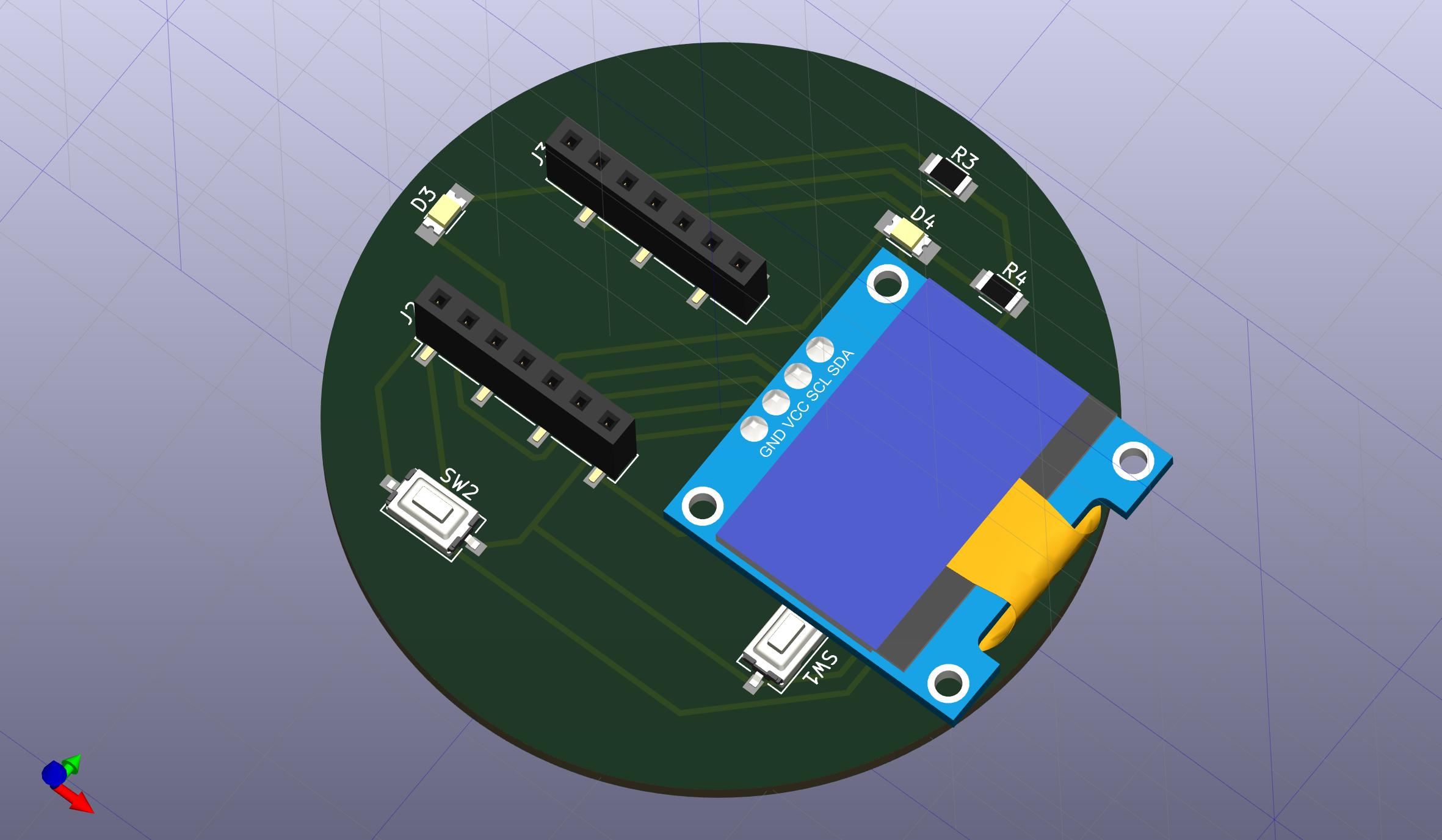
Step 1: 3D CAD Visualization - Generating a 3D preview of the trace layout and footprint spacing to check component clearances prior to exporting toolpaths.
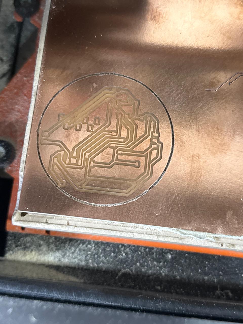
Step 2: Substrate Milling - The raw copper board fresh off the Roland SRM-20 milling machine, showing clean trace isolation and cleared isolation channels.
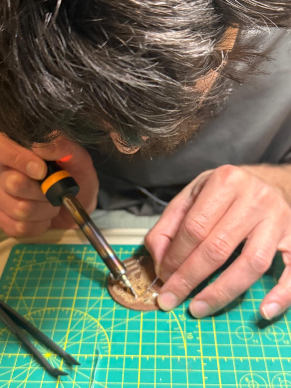
Step 3: Component Assembly - Hand-soldering the micro-components, headers, and the main microcontroller using fine-gauge solder wire and flux core.
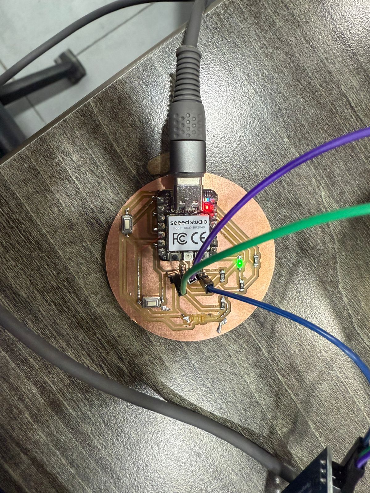
Step 4: Final Functional Board - The fully populated output visualizer board, ready for firmware flashing and hardware testing loops.
4. Resources & Assets
References
Source Files