Week11
Networking and Communications
Group assignment:
- Send a message between two projects
- Document your work to the group work page and reflect on your individual page what you learned
Individual assignment:
- design, build and connect wired or wireless node(s) with network or bus addresses and a local input and/or output device(s)
The supplementary explanation from Saheen
Hi everyone! Just a small clarification about the Networking and communication Week assignment requirements:
The goal is to design, build, and connect at least two embedded nodes (node-to-node communication). Each node should have:
- its own network or bus address
- at least one local input and/or output device
- and communicate directly with another node
The connection medium is flexible 👍 — it can be:
- wired (UART, I2C, SPI, CAN, etc.)
- wireless (WiFi, BLE, ESP-NOW, LoRa, RFID, etc.)
- mesh systems (Meshtastic, MeshCore, etc.)
- internet-based protocols like MQTT, HTTP, Matter ( only if communication is directly between devices )
🚫 Avoid using cloud/virtual intermediary platforms that store or route data (e.g., Firebase, Blynk, ThingSpeak, etc.), since these are not considered direct node-to-node communication.
So the key requirement is two embedded devices communicating with each other, not just a device talking to a computer, phone, or cloud service.
Group assignment
Our group assignment is on lab’s page.
Individual assignment:
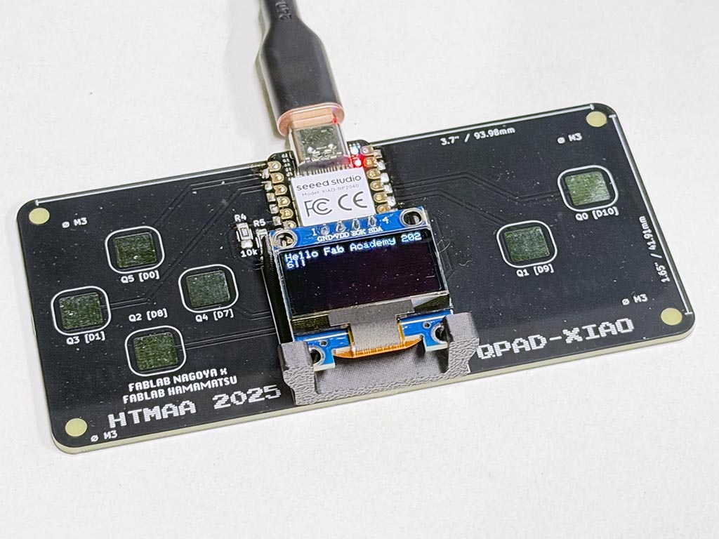
Take-san ordered QPAD-xiao PCB and gave it to me, so I assembled it. So, I used QPAD to finish my week 11 assignment. The design file of QPAD-xiao can be found in the repository.
I wrote very simple sketch that read string from USB-serial and draw it on OLED through I2C. USB-serial is local input, OED is local output in this project.
I refer test_display_RP2040.ino and got how to handle this OLED on Arduino IDE, and added some code that read the string through USB-serial from personal computers. I2C is the bus that use addresses. For the SSD1306, the slave address is either “b0111100” or “b0111101” by changing the SA0 to LOW or HIGH. The board I used was “b0111100” (0x3C) one.
#include <Wire.h>
#include <Adafruit_GFX.h>
#include <Adafruit_SSD1306.h>

#define SCREEN_WIDTH 128 // OLED display width, in pixels
#define SCREEN_HEIGHT 64 // OLED display height, in pixels
#define SCREEN_ADDRESS 0x3C // 0x3D or 0x3C depending on brand
Adafruit_SSD1306 display(SCREEN_WIDTH, SCREEN_HEIGHT, &Wire, -1, 1700000UL, 1700000UL);

String incomingstring;

void setup() {
  Serial1.setRX(1); // assigning P1 for UART RX
  Serial1.setTX(0); // assigning P0 for UART TX
  Serial1.begin(9600); // going to communicate with 9,600bps

  delay(50);

  /* initializing display */
  display.begin(SSD1306_SWITCHCAPVCC, SCREEN_ADDRESS);
  display.clearDisplay();
  display.display();
  display.setTextSize(1);
  display.setTextColor(SSD1306_WHITE);
}

void loop() {
  if (Serial1.available() > 0) {
    incomingstring = Serial1.readStringUntil('\n'); // reading string until Line Feed
    display.clearDisplay();
    display.setCursor(0, 0);
    display.print(incomingstring); // display read string on OLED
    display.display(); // let the display go
  }
}
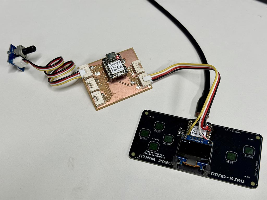
Since the key requirement is “two embedded devices communicating with each other”, I wrote following code abd connected QPAD and my dev board by wire.
int Pot = 0;
char buf[44];

void setup() {
  Serial1.setRX(1); // assigning P1 for UART RX
  Serial1.setTX(0); // assigning P0 for UART TX
  Serial1.begin(9600); // going to communicate with 9,600bps
}

void loop() {
  Pot = analogRead(A1);
  sprintf(buf, "Pot: %d", Pot); // making a string to send
  Serial1.println(buf); // send strinf and line feed
  delay(500);
}
To be easy to recognize, I powered my dev board from QPAD. My board send a analog value of connected potentiometer and send it to QPAD through UART. QPAD receive read values and print it on it’s OLED.
Unfortunately, there are nothing special I learned from the process finishing this assignment. Sorry for being cheeky.
I²C
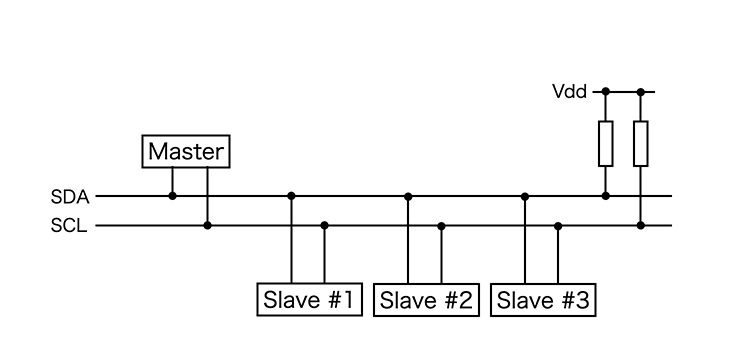
I²C (Inter-Integrated Circuit; pronounced I-squared-C) is synchronous multi-slave serial communication bus invented by Philips Semiconductors (now NXP Semiconductors) about half century ago.
One of the biggest advantages of I²C is its simplicity at the hardware level. It requires only two signal wires to communicate between multiple devices. One signal wire is SDA (Serial Data Line), the line used for the master and slave to send and receive data. The other signal wire is SCL (Serial Clock Line), the line that carries the clock signal, always generated by the master to synchronize data transfers. Since there are SCL, I²C is a synchronous communication bus.
I²C devices cannot actively drive the bus lines HIGH. They can only pull them LOW. Therefore, the bus requires pull-up resistors connected to a positive voltage supply. On QPAD, we can find two pull-up resistors left next to XIOA. When no device is communicating, the lines are pulled high by pull-up resistors.
Since I²C is a registered trademark owned by NXP Semiconductors, some companies uses TWI (Two-Wire Interface) to avoid paying trademark fees. Some of those implementation are not using true open-drain architecture, using emulated open-drain or in the worst case using true push-pull. We need to take care when we use TWI.
On I²C, every slave on the bus has a unique hardcoded or configurable address. So the master sends the 7-bit address of the specific slave it wants to communicate with. At this time, I designated display’s address as #define SCREEN_ADDRESS 0x3C in the sketch. By using this address, Adafruit_SSD1306 library start initializing display through Wire library. Wire is a bundled Arduino library that handle I²C communication. If you want to learn about I²C more, there are Inter-Integrated Circuit (I2C) Protocol page on Arduino docs.
Problem I had.
The PCB take-san provided doesn’t have drill holes. So I cut tip of pin header for about one mm and soldered on the surface of top side of PCB. It works because traces of thie board are only on top side of this PCB.
Checklist
- Linked to the group assignment page
- Documented your project and what you have learned from implementing networking and/or communication protocols.
- Explained the programming process(es) you used.
- Ensured and documented that your addressing for boards works
- Outlined problems and how you fixed them.
- Included design files (or linked to where they are located if you are using a board you have designed and fabricated earlier) and original source code.
- Included a ‘hero shot’ of your network and/or communications setup