6. Electronics design
Assignments and Assessment this week
Group assignment
- Use the test equipment in your lab to observe the operation of a microcontroller circuit board (as a minimum, you should demonstrate the use of a logic analyzer)
- Document your work on the group work page and reflect what you learned on your individual page
Individual assignment
- Simulate a circuit
- Use an EDA tool to design a development board that uses parts from the inventory to interact and communicate with an embedded microcontroller
- extra credit: try another design workflow
- extra credit: design a case
Learning outcomes
- Select and use software for circuit board design
- Demonstrate workflows used in circuit board design
Have you answered these questions?
- Linked to the group assignment page
- Documented what you have learned in electronics design
- Checked your board can be fabricated Explained problems and how you fixed them.
- Included original design files (Eagle, KiCad, etc.)
- Included a ‘hero shot’
Group Assignment
Here is a group assignment page
Research
Functions of Each Component Discrete Components You Should Know Roughly
Resistor Capacitor Inductor Diode Transistor Operational Amplifiers
Useful link
Explains the foundation of electric circuits by @qwer123123
Resister
Generates voltage by preventing the flow of electrons (current).
Capacitor
Stores charge (electrical energy). Resists sudden changes in voltage. Direct current stores electricity without passing it. Active current discharges the previously stored electricity as the direction of the current changes.
Inductor
Stores electricity by converting it to magnetism. An element that does not like change. It resists sudden changes in current. For this reason, unlike capacitors, it passes DC but not AC. Also used in motors and transformers.
(Vacuum tube)
An element that functions similarly to semiconductors, used before semiconductors became mainstream. Utilizes electrons emitted from a heated filament in a vacuum. Requires a high voltage of over 100V. Large, heat-generating, and power-hungry.
Semiconductors
Compared to vacuum tubes, semiconductors are smaller, lighter, and more energy-efficient, allowing for the integration of a larger number of elements. They utilize the electrons and holes inside semiconductors such as silicon. They operate at low voltages of just a few volts and do not need to heat up.
Diodes
Limit the direction of current flow. They are also used to generate constant voltages. LEDs Zener diodes Schottky diodes
Transistors
Amplify current; perform electrical switching. The ATMEGA328p, ESP32C3, and RP2040 are made up of a collection of small transistors. Crystals (quartz crystal oscillators) Power semiconductors Bipolar transistors, Power MOSFETs, IGBTs
Operational amplifier
Amplifies voltage
simulate a circuit
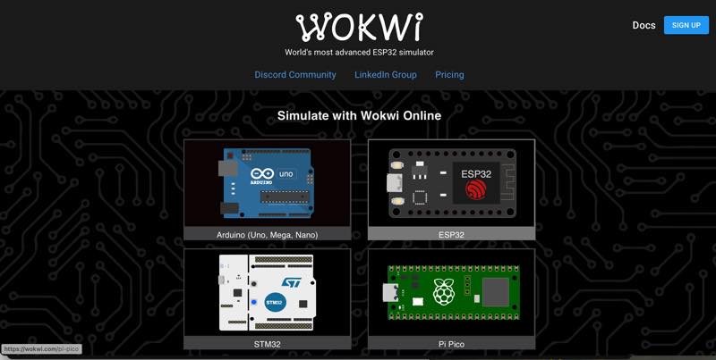
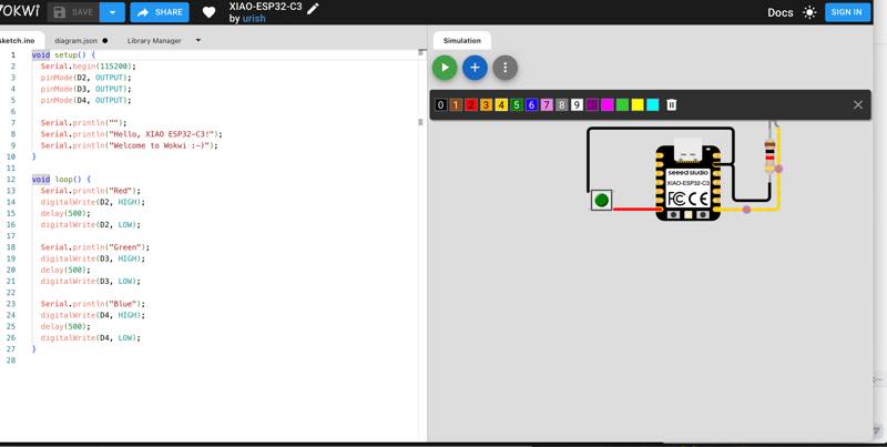
There are several ways to do this, but this time I tested two web-based methods. First, I tried Wokwi, which I used in Week 4.
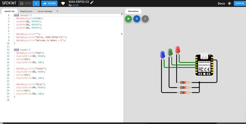
select ESP32 C3 XIAO
By the way, the previous simulation can be found here: Simulate with Wokwi Online The advantages of this method are that it’s web-based, so no dedicated software is required. You can also check the program you’ll be putting into the microcontroller, so you can see how the circuit will behave.
put the Components
Wire ring
set Programing and lunning the program writn by Neil Gershenfeld hello.button-blink.C3.ino
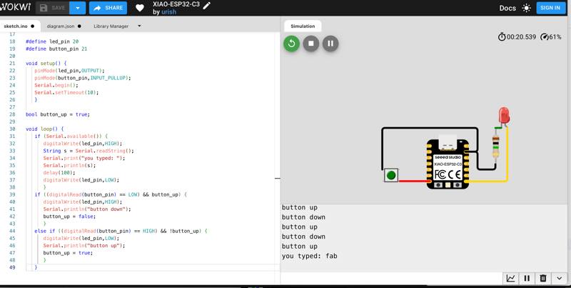
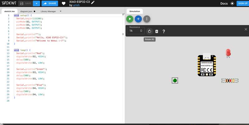
The disadvantage is that it can’t simulate analog behavior (such as the current flow), so adding a resistor won’t simulate properly. Even connecting a 1MΩ resistor, which is impossible in reality, will cause the LED to light up. This week used Wokwi data
In contrast, Electronic Circuit Simulator Applet by Paul Falstad even reproduces analog signal behavior. It can also simulate AVR programs. However, since the ESP32 and RP2040 are not in the lineup, it’s not possible to experiment with them. It also requires a certain level of prior knowledge of the components, making it difficult for beginners to use alone. However, once you’ve mastered it, it becomes an extremely powerful tool. LCR Simulate
By using these simulation software and prototyping on a breadboard, we can confirm the behavior and actually write out the circuit. It’s possible to create a circuit board by etching a handwritten design as a mask and melting the copper foil, as in the old days, but because disposing of the waste liquid is difficult, we decided to create data that would allow us to burn off the copper foil with a laser or use CNC milling to remove it from the board.
another simulate diode Build, program, and simulate hardware in the browser. diode project
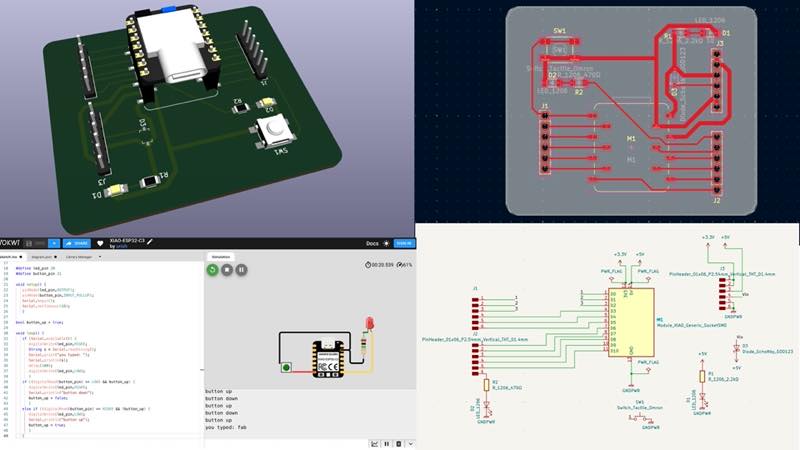
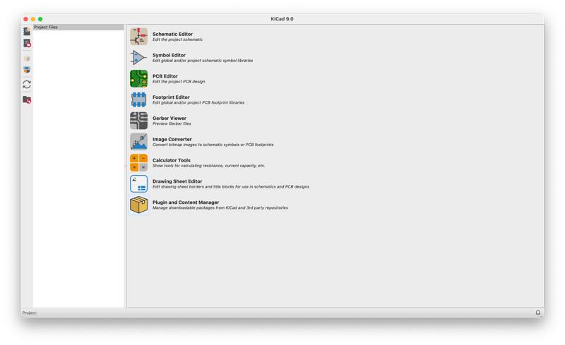
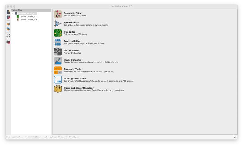
Circuit Board Fabrication (ECAD)
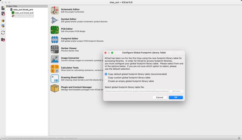
The software used for this project is free circuit design software called Kicad.
Like many other electrical CAD programs, the process involves creating a circuit board by creating a component connection diagram, checking the connections, arranging the components, and verifying the circuit rules.
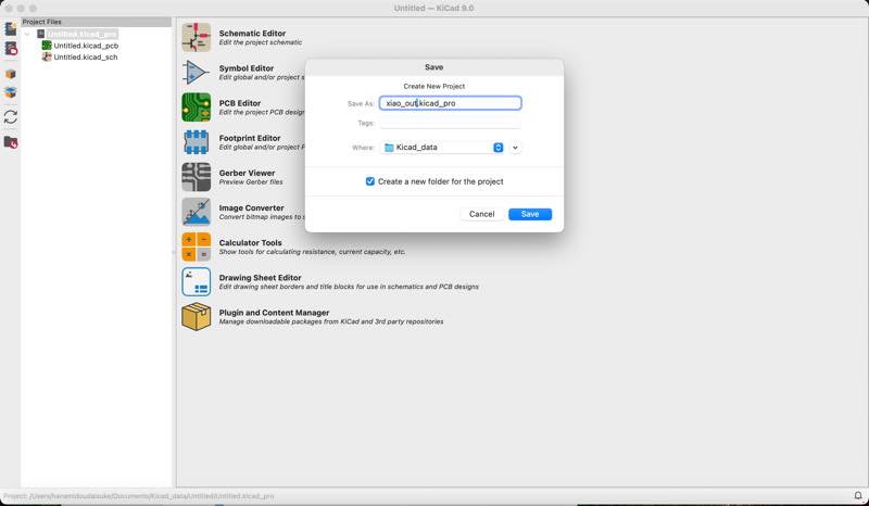
Open new project
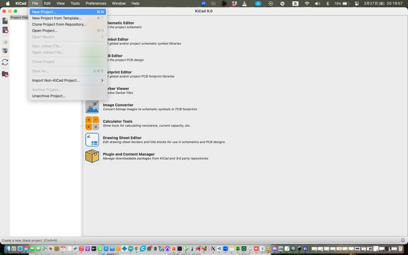
And save as Give it a name
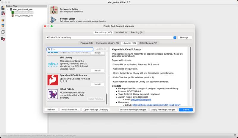
Download Plugin
KiCad FabLib Components plugin This plugin adds electronic components to the default state.
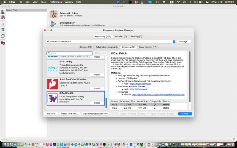
The plugin will not be activated unless you install and apply it.
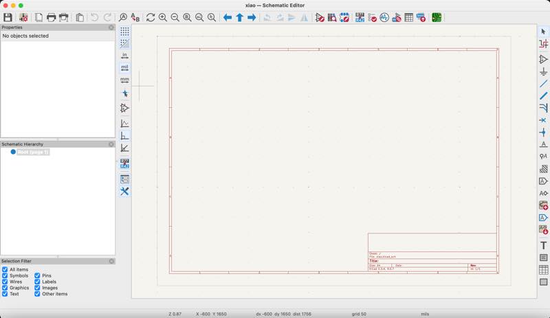
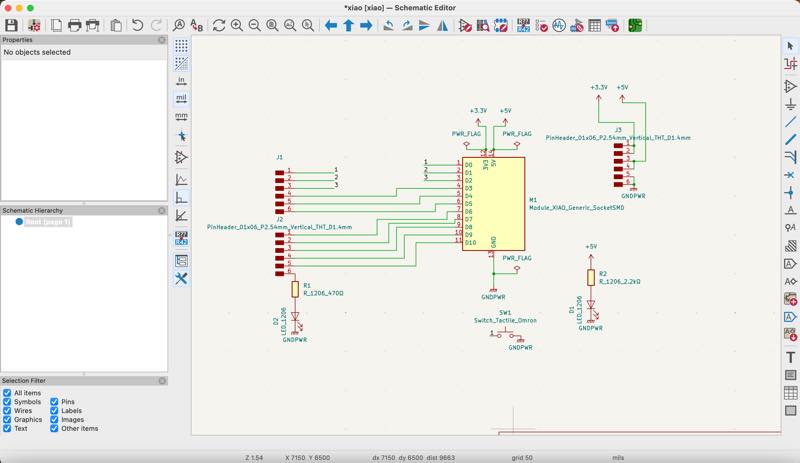
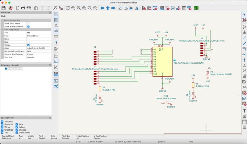
Schenatic Editor
Edit the Project Schematic check OK to the default
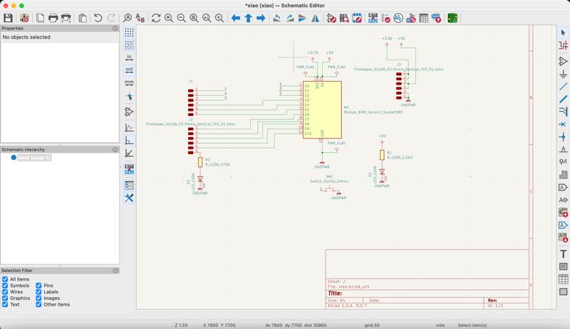
Select the Schematic symbols
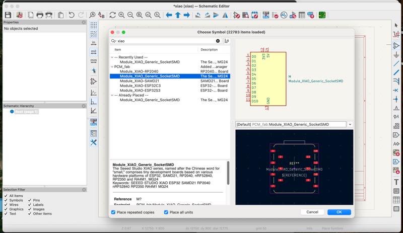
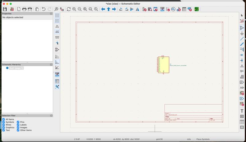
Select the xiao put it
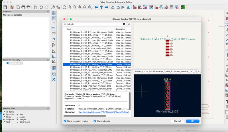
Select pin header 1X6
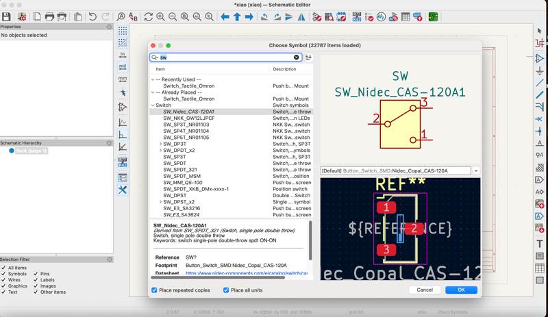
Select push switch
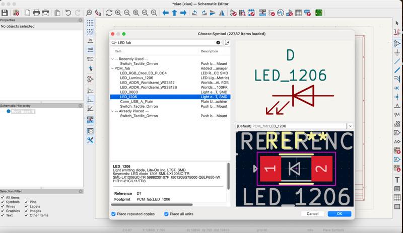
Select 1206 LED
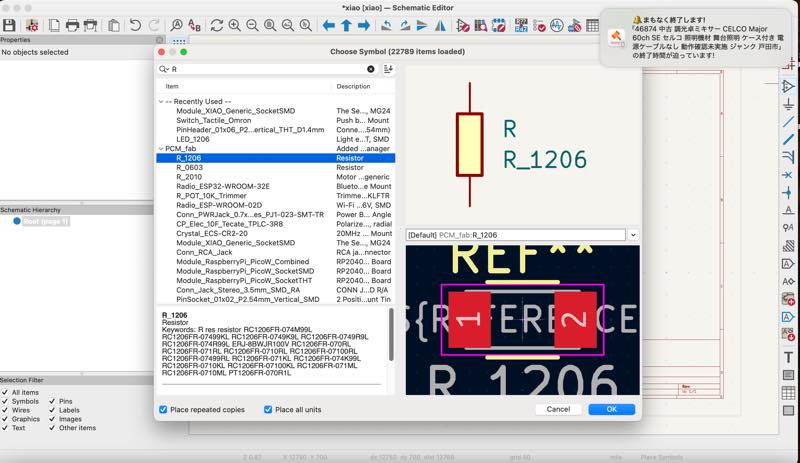
Select 1206 Register
Connect the circuit
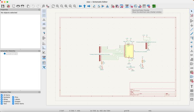
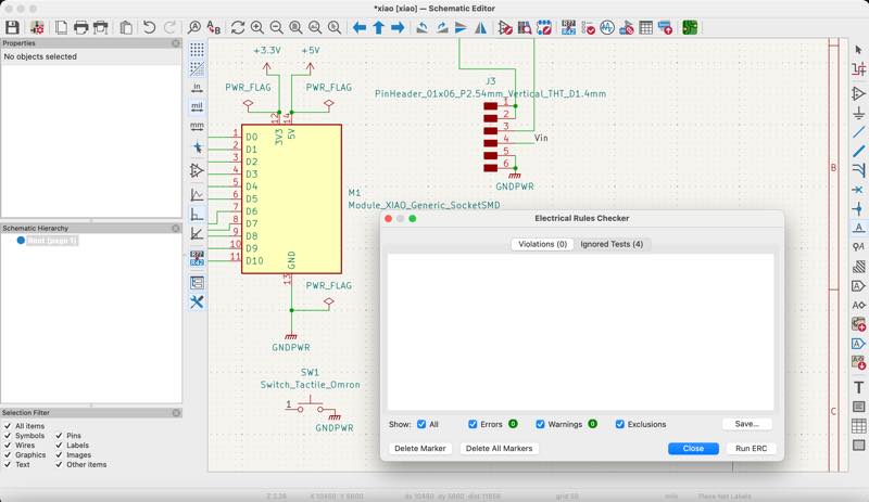
Checing ERC
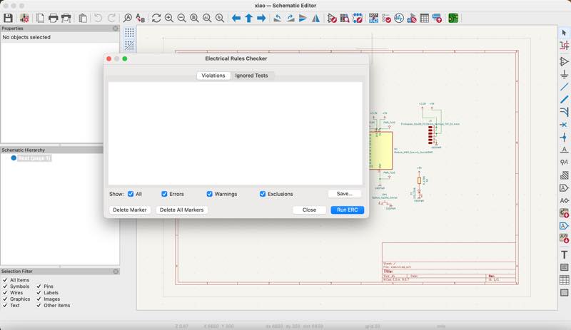
Press RUN ERC
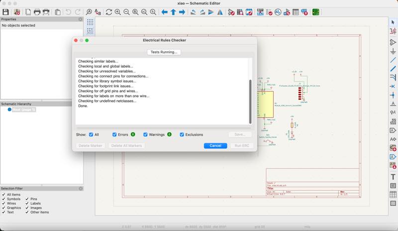
An error occurred.
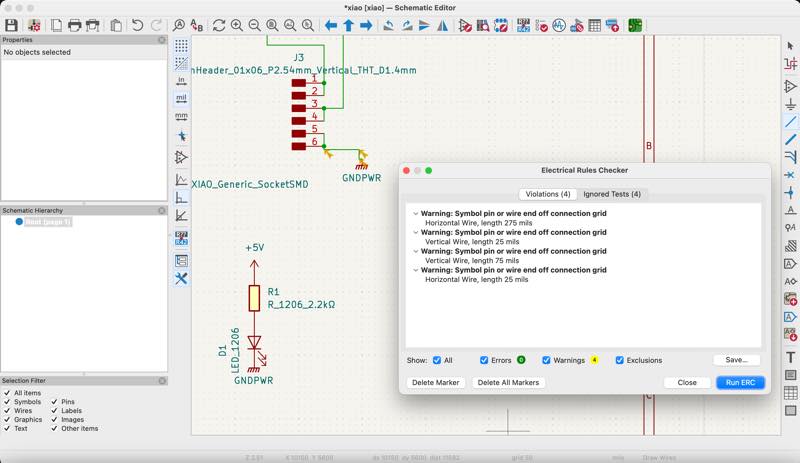
There is an error in the area indicated by the arrow.
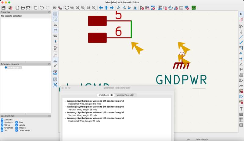
It seemed like the connection wasn’t working properly, so I moved the parts and reconnected them.
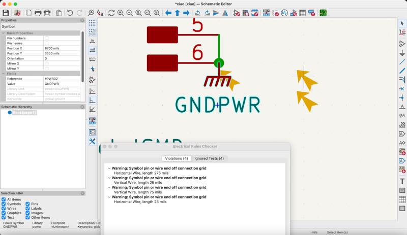
Trying again the ERC
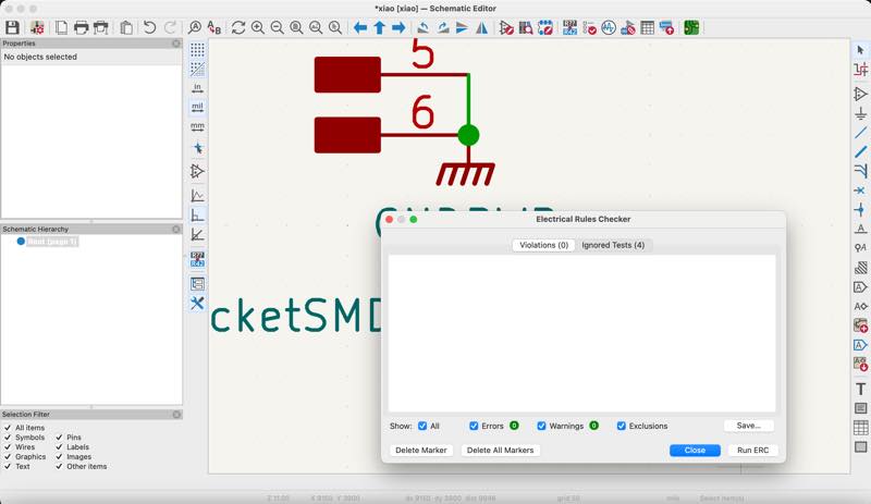
ERC completed.
Switch to the PCB editor
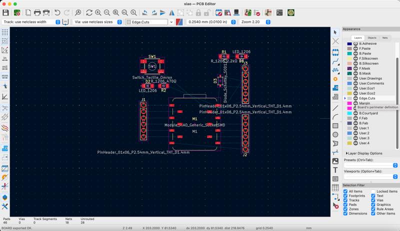
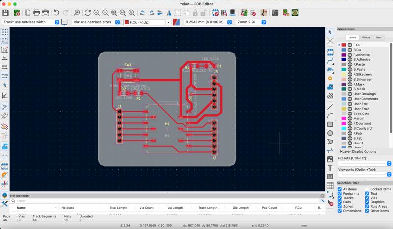
PCB Editor
Edit the project PCB design
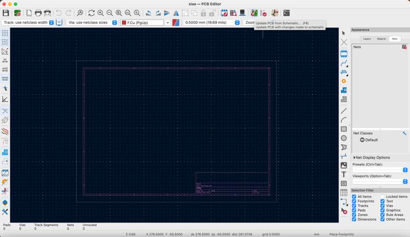
Update fo PCB from schematic
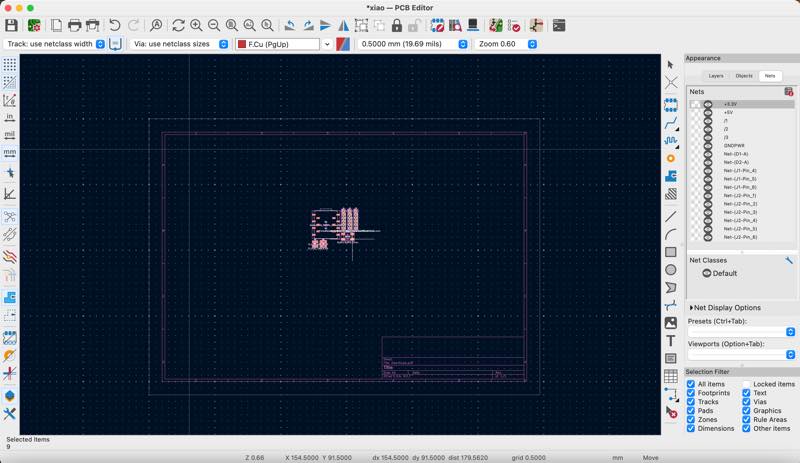
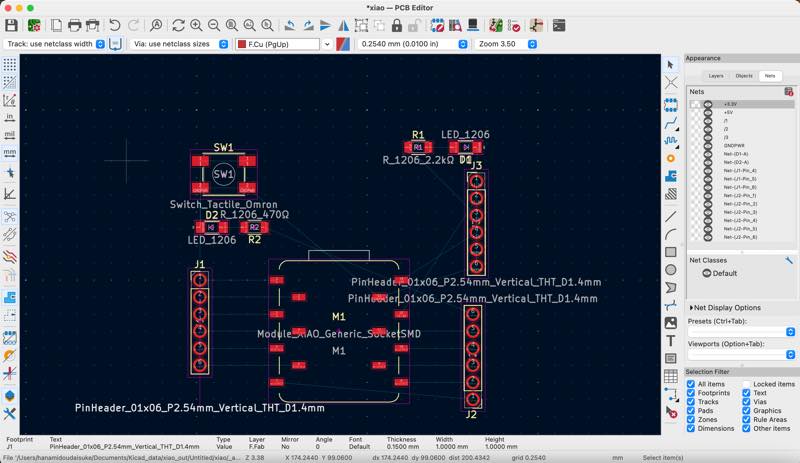
Place the parts
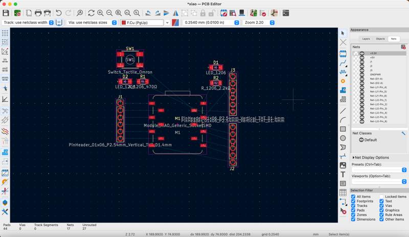
Rearrange the parts
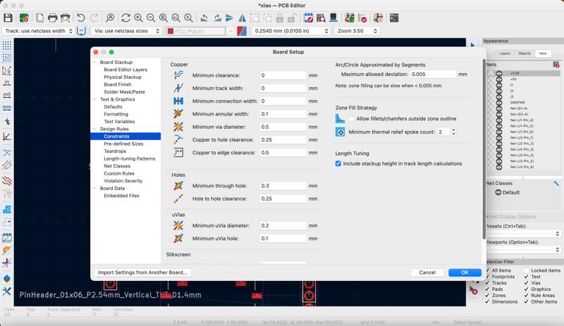
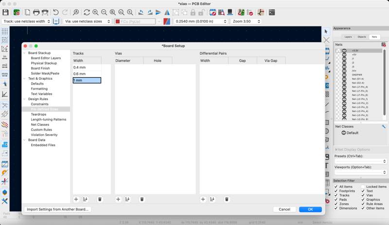
Select “Constraints” and set the clearance and minimum track width.
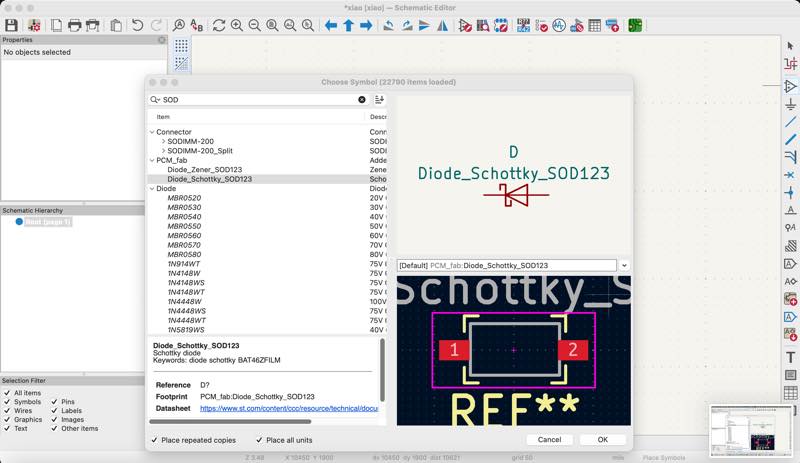
I was told that it would be better to add a diode to the 5V input, so I will add one.
The wiring was done and the ERC was OK.
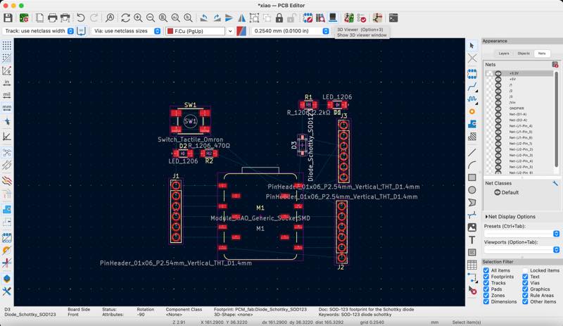
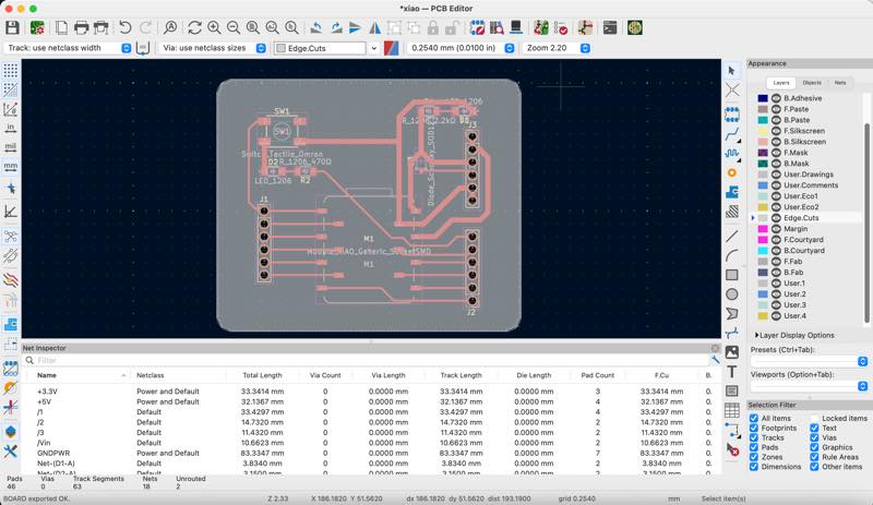
Parts placement complete
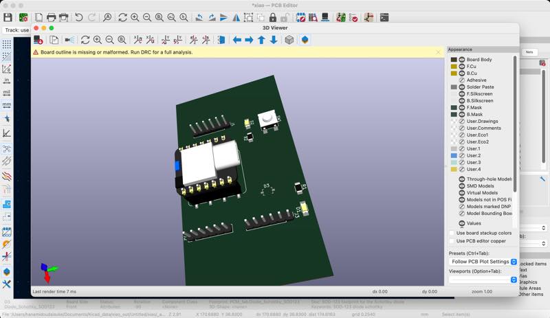
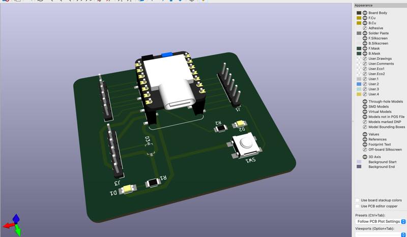
3D
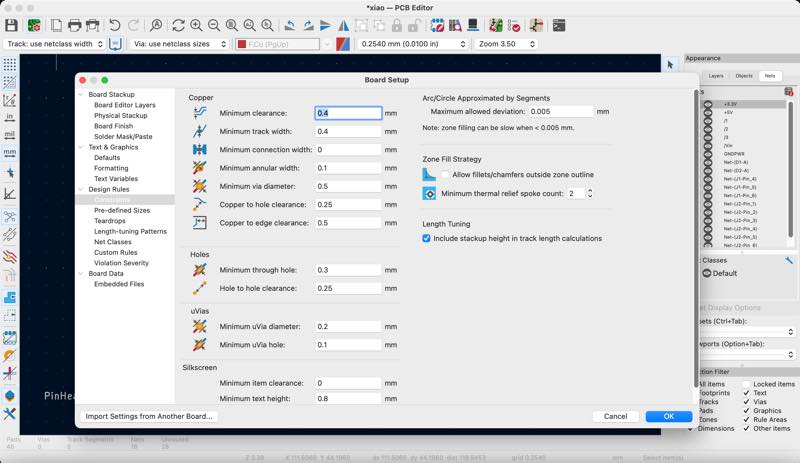
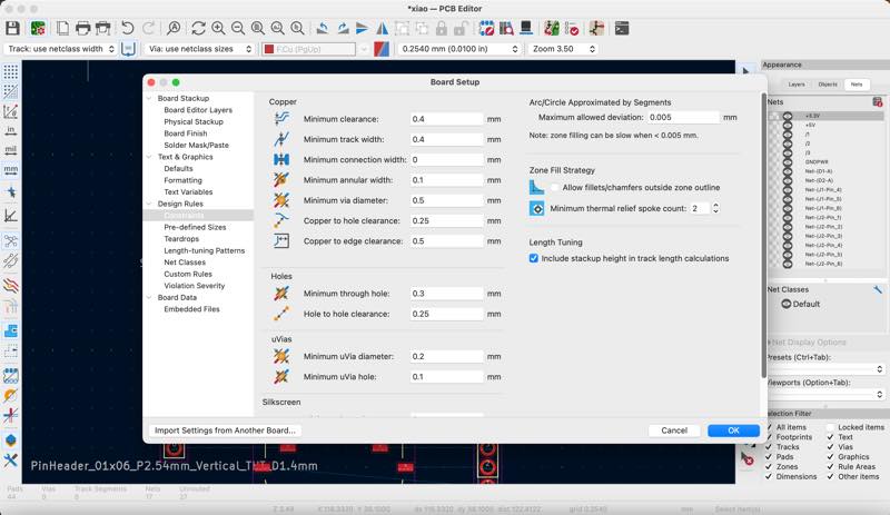
Open the settings again and this time set the wiring width.
After doing some basic wiring, I learned how to create the outer casing.
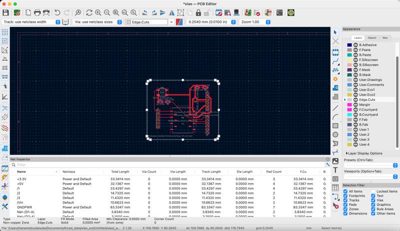
Field zone set
DRC
Perform a Design Rule Check (DRC).
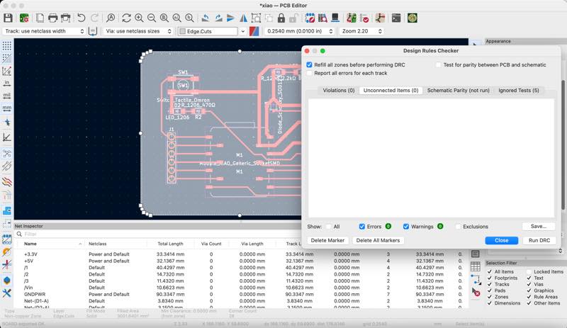
No problem
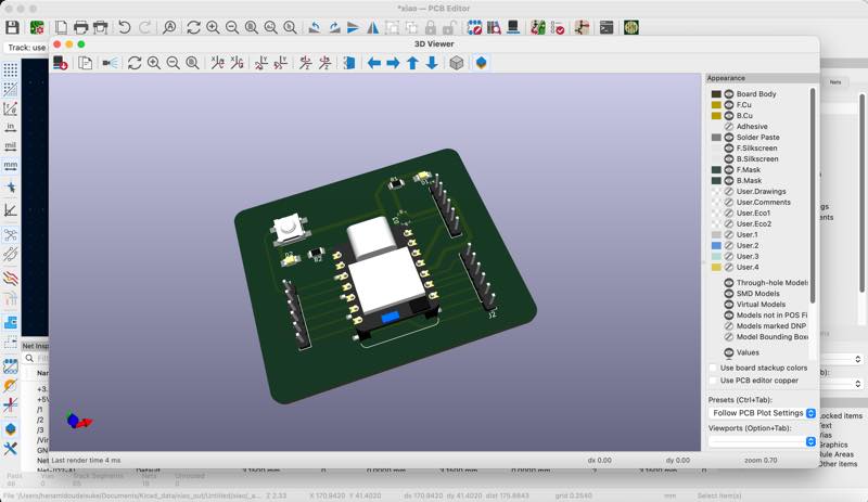
Final 3D design
I try aut root conecting by Freerouting
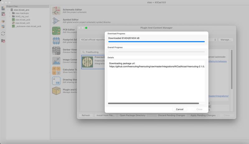
Installing plugin Freerouting
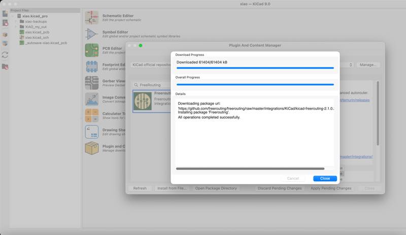
select Freerouting
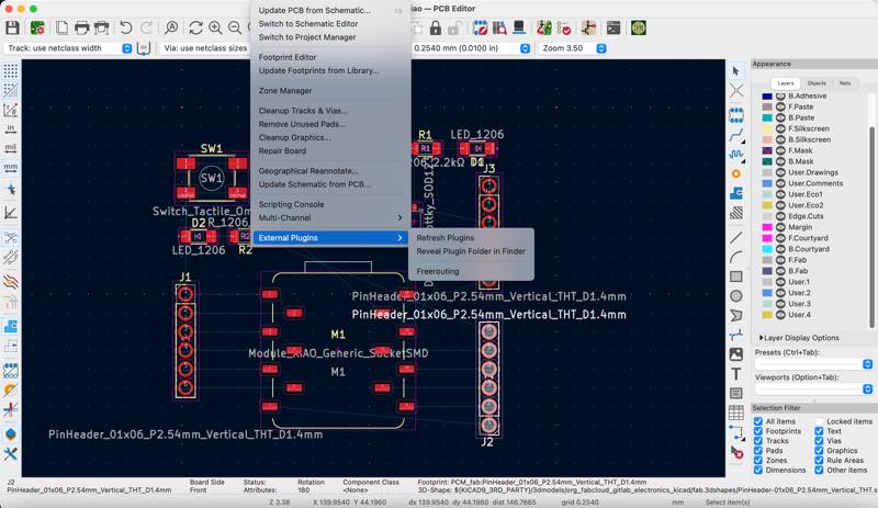
not working
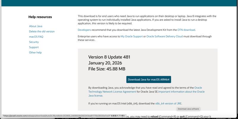
installing java 8
makeing icon
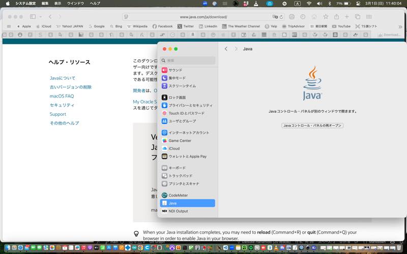
installing finished java 8
Nothing happened this week in the end.
Not working Freerouting becouse I have a lot of java
Uninstall Oracle Java using Terminal
- Click on the Finder icon on the Dock
- Click on the “Utilities” folder
- Double-click the “Terminal” icon
- Copy and paste the following command into the terminal window:
nextsudo rm -fr /Library/Internet\ Plug-Ins/ JavaAppletPlugin.plugin sudo rm -fr /Library/PreferencePanes/JavaControlPanel.prefPane sudo rm -fr ~/Library/Application\ Support/Oracle/Javarm -r ~/"Library/Application Support/Oracle/Java"
Installing JDK
Java SE Development Kit 25.0.2
I can use Freerouting at week11!
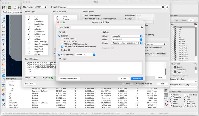
How to jlcPCB settings
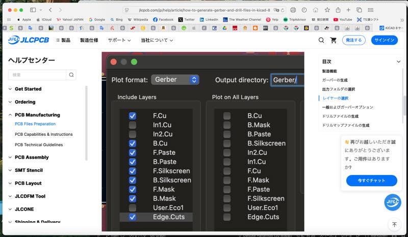
Out put .gbr
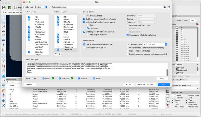
Out put .drl
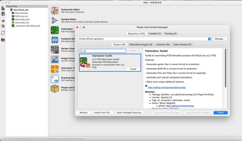
I have plugin of jlcpcb
Fablication tool kit is one push output .gbr and .drl in to .zip file
install plugin
out put to .zipfile in the production folder
in jlcpcb fab
A walk through a giant printed circuit board factory in China by Robert Ferane
out put .png file by gerber2png
Out put GerBer by Fablication tool kit
gerber2png With Safari, the zip file was unzipped and downloaded, preventing me from successfully installing it into KIcad. With Chrome, the zip file downloaded correctly and the installation worked properly.
2026/3/24 in to kicad plugin
schematic
PCB
3D
Chip Component Sizes and Size Names
| Length [mm] | Width [mm] | JIS Metric Code | EIA Imperial Code |
|---|---|---|---|
| 0.4 | 0.2 | 0402 | 01005 |
| 0.6 | 0.3 | 0603 | 0201 |
| 1.0 | 0.5 | 1005 | 0402 |
| 1.6 | 0.8 | 1608 | 0603 |
| 2.0 | 1.25 | 2012 | 0805 |
| 3.2 | 1.6 | 3216 | 1206 |
| 3.2 | 2.5 | 3225 | 1210 |
| 5.0 | 2.5 | 5025 | 2010 |
| 6.4 | 3.2 | 6432 | 2512 |