ELECTRONIC DESIGN
Tools

Installation
The first step is to install a suitable software for circuit design. In my case, I used KiCad, as it is an open-source tool that allows seamless integration with other platforms for PCB post-processing.
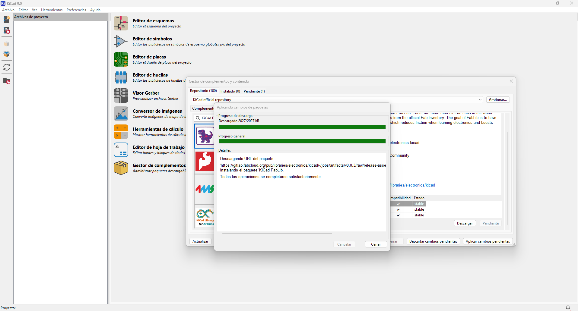
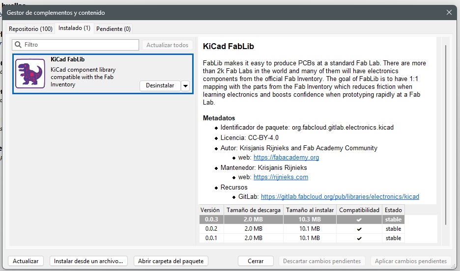
I´ve installed the KiCad FabLib library using the Plugin and Content Manager. This library includes standardized symbols and footprints that correspond to the components commonly available in Fab Labs, making it easier to move from design to physical fabrication.
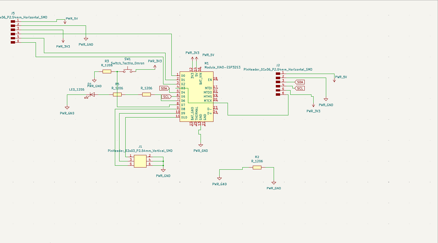
Electronics Schematic
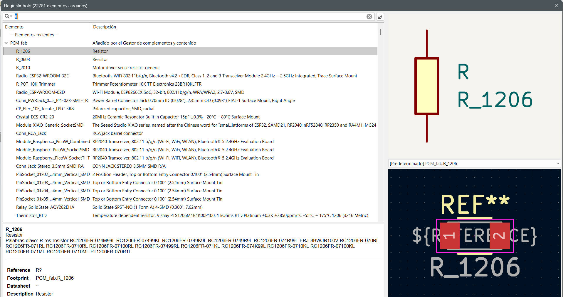
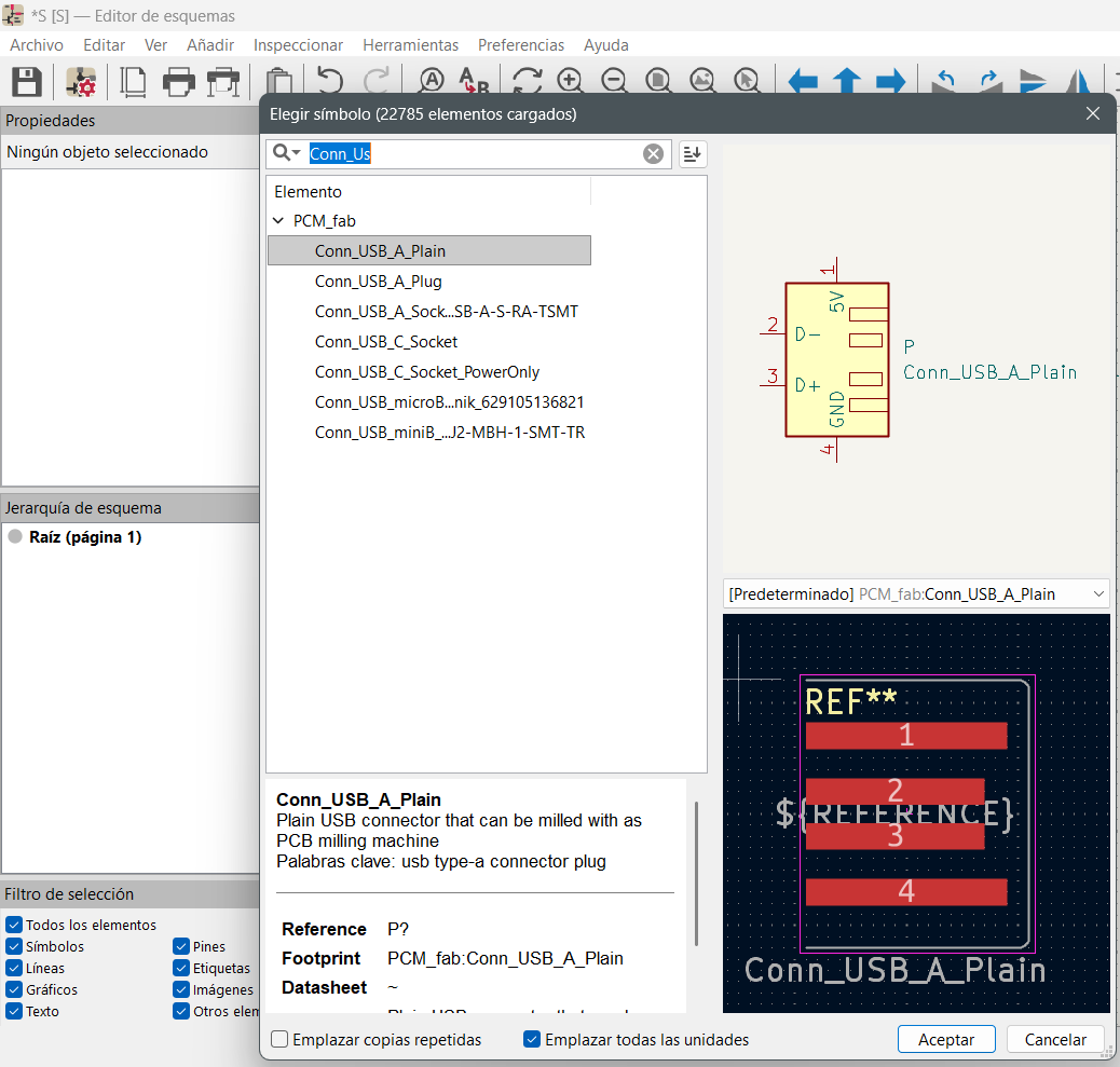
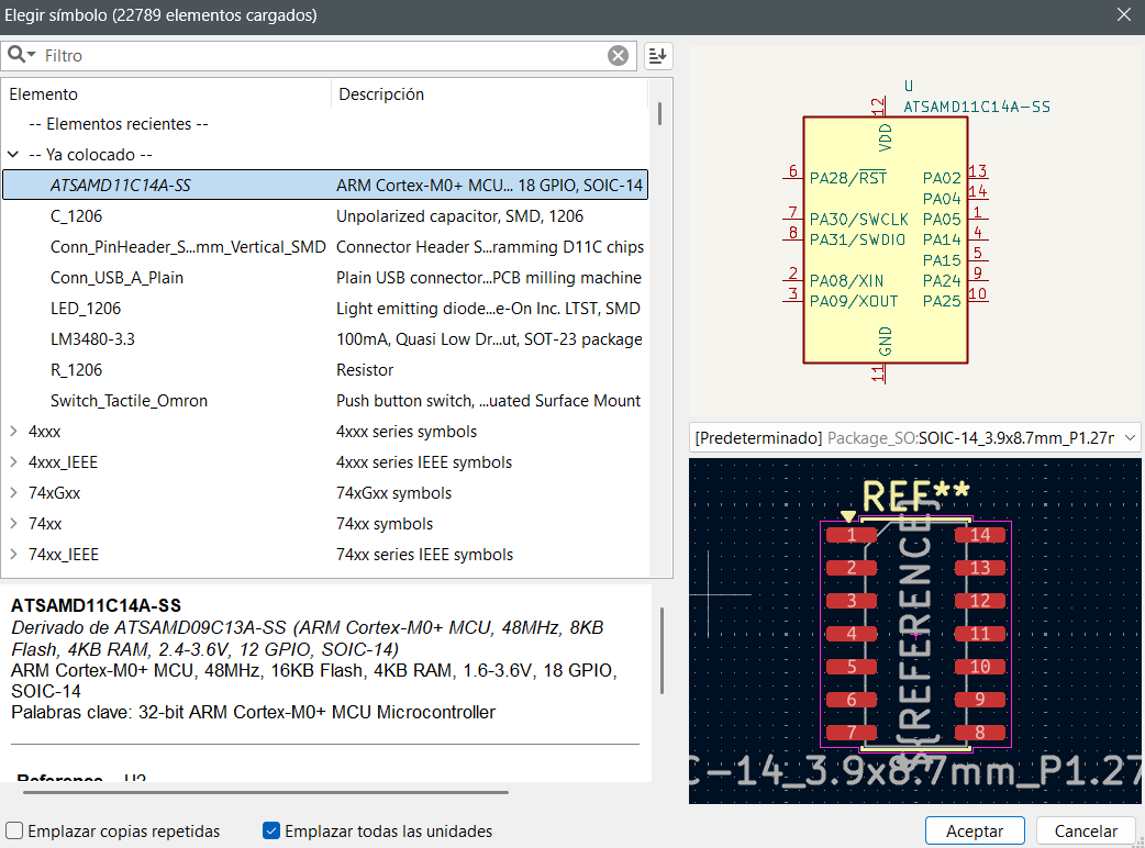
Once the Fab library was installed, I began selecting the required components directly from the symbol editor, which allows the use of compatible footprints.
This workflow makes the design process faster as the selected components are already aligned with fabrication constraints during the PCB design stage.
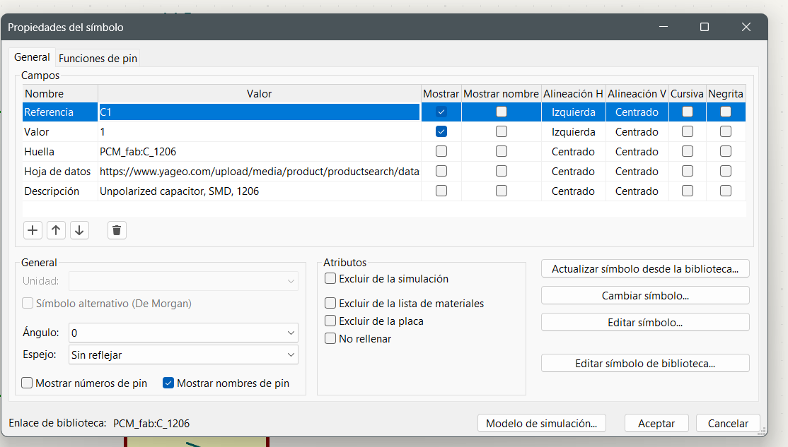
You can also modify the values of the components directly within their properties, allowing you to adjust parameters such as resistance, capacitance, or other specifications according to the design requirements.
The following schematic was developed based on previously used designs in Fab Academy, built around a SAMD11C microcontroller. It represents a basic system that integrates power supply, USB communication, and input/output components. Working with this design helped me understand the PCB design workflow, as I did not have prior experience in this type of development. Around it, different subsystems are connected to enable its operation:
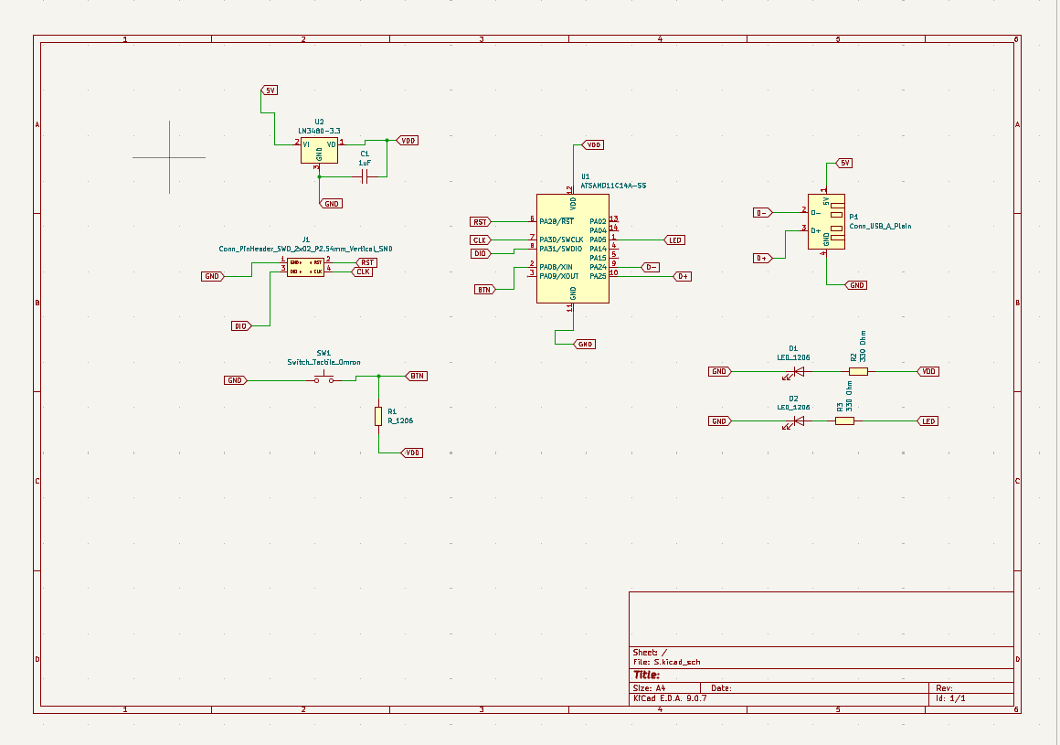
- Power Supply System: The circuit receives 5V from the USB connector, which is regulated down to 3.3V (VDD) using a voltage regulator (LM3480). This voltage powers the microcontroller and the rest of the components. A capacitor is included to stabilize the voltage and reduce noise.
- USB Communication: The USB connector provides both power (5V and GND) and data lines (D+ and D-), allowing communication between the board and a computer.
- Programming Interface (SWD): A pin header is included for SWD programming, using signals such as RST, CLK, and DIO.
- Input System (Button): A push button is connected to one of the microcontroller pins. A resistor acts as a pull-up, ensuring a stable logic state when the button is not pressed.
- Output System (LEDs): LEDs with current-limiting resistors are included, serving as visual indicators for testing and verifying the system’s operation.
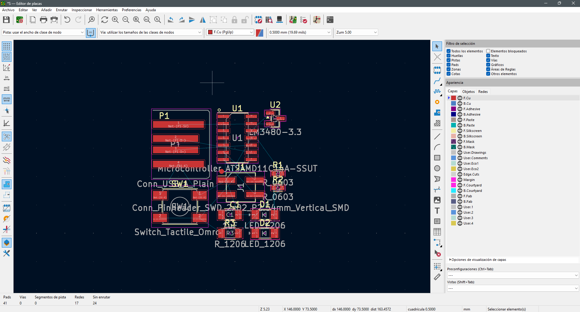
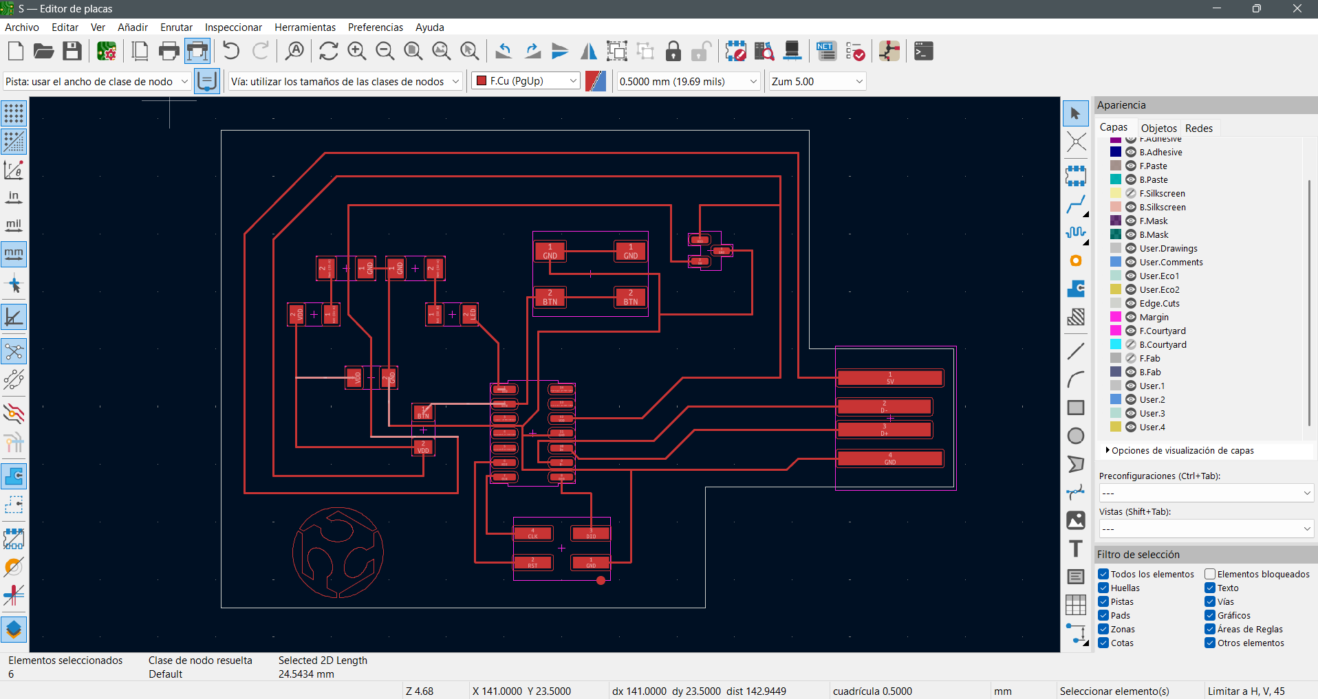
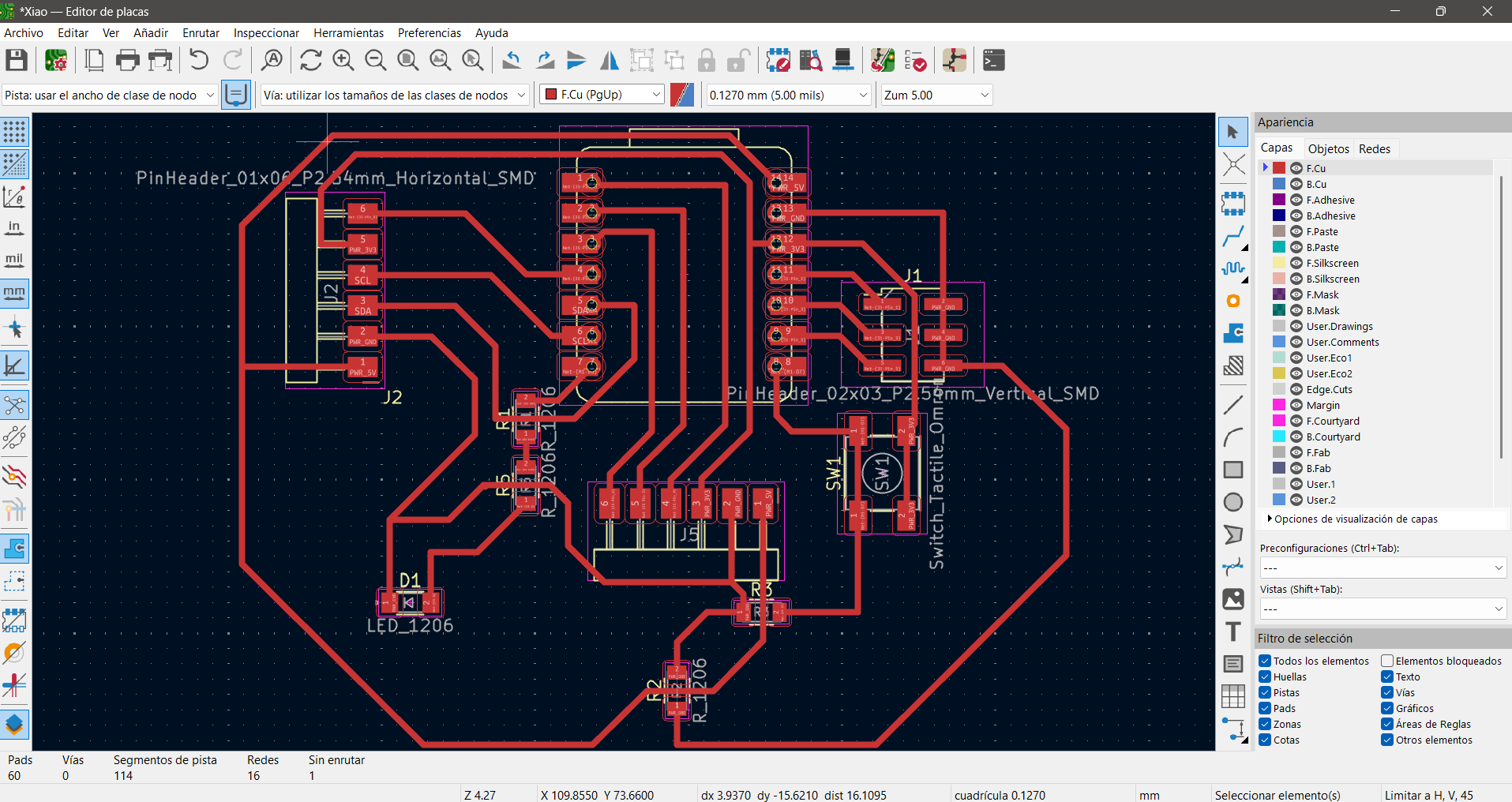
The schematic can be transformed into a PCB design using the board editor. All components are imported with their corresponding footprints in an unorganized layout, which becomes a challenge in the workflow, as it requires proper arrangement to route traces efficiently and avoid unnecessary crossings.
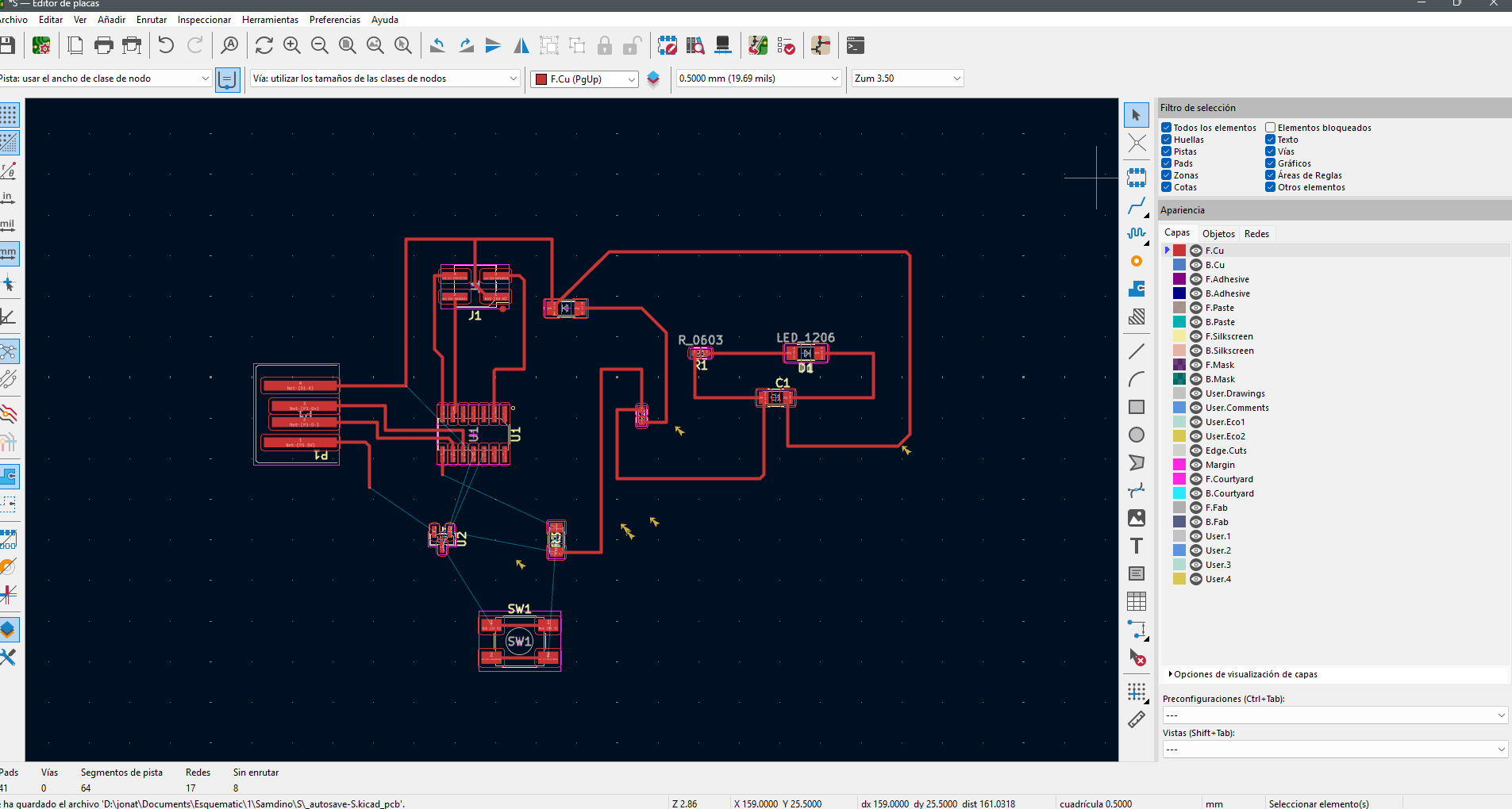
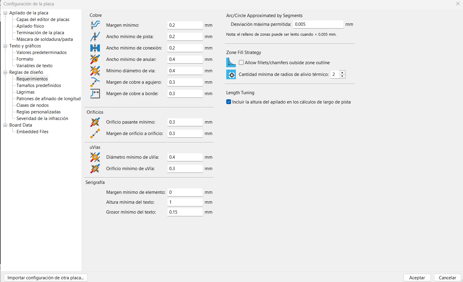
In my case, I had to modify the trace design parameters, since with the default configuration it was almost impossible to connect all the components on a single board. However, to solve this issue I adjusted the design rules to connect all the components. This change affects the fabrication process, because reducing the trace width and spacing requires the use of a 0.2 mm milling bit in order to mill the traces properly.
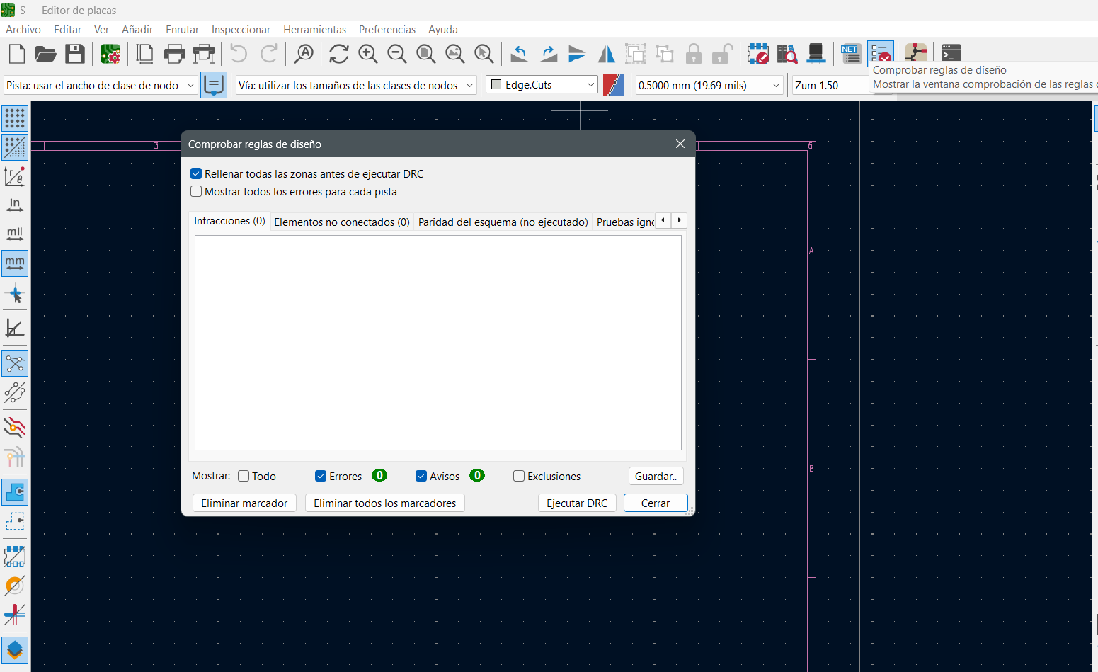
Before exporting the design, it is necessary to verify that the PCB has no connection errors or design rule violations using the Design Rule Check (DRC) tool.

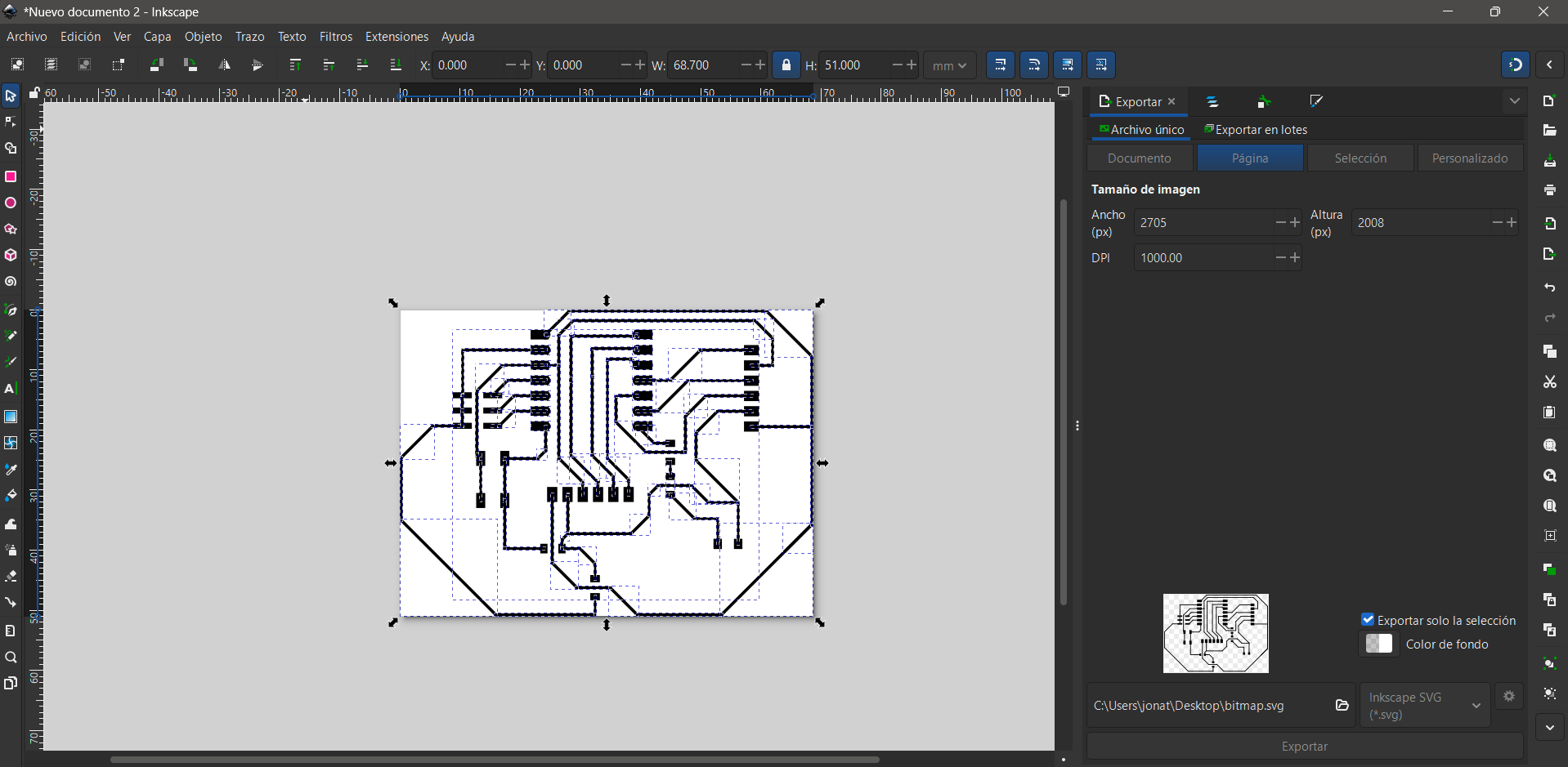
Finally, I used the 3D viewer to visualize and verify the dimensions of the PCB.
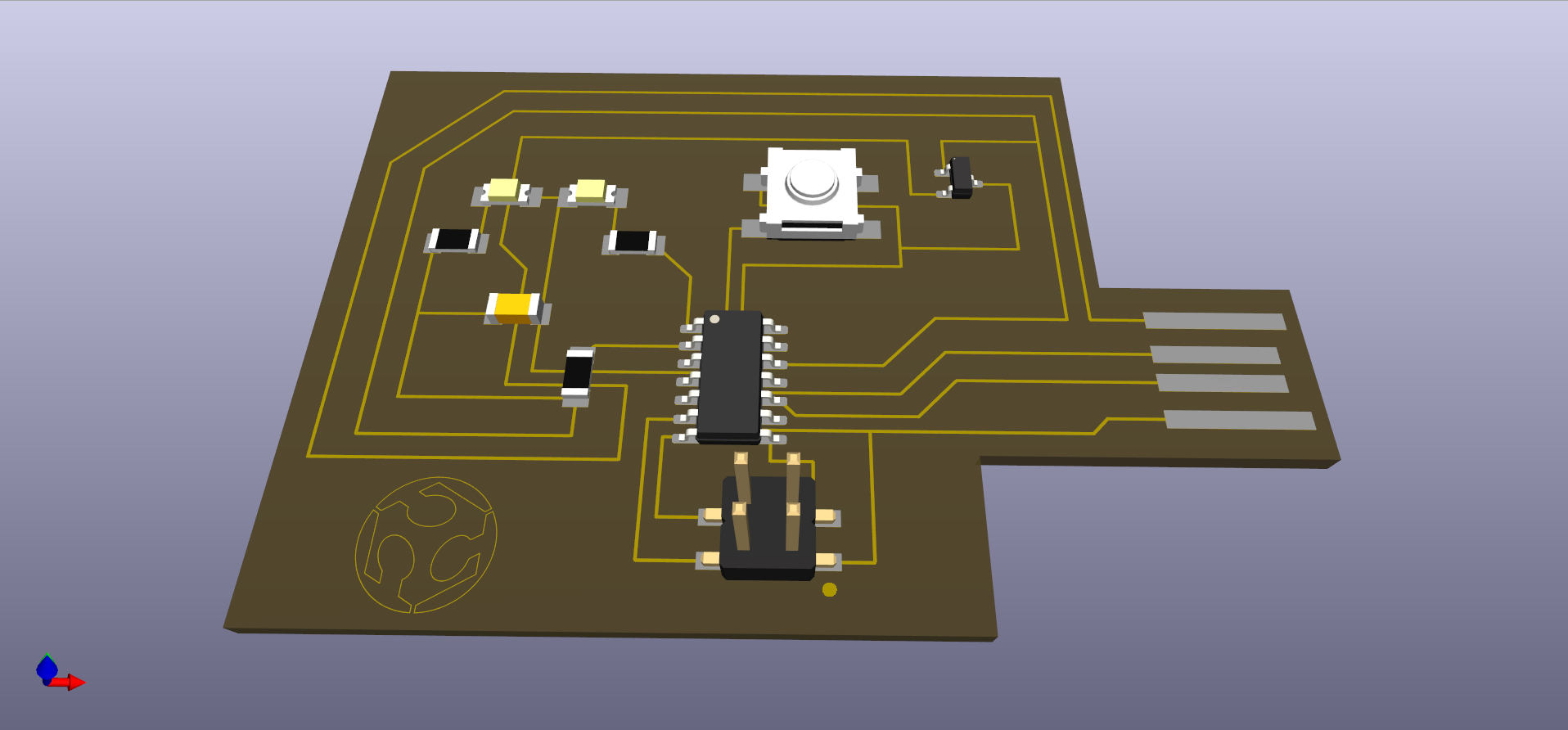
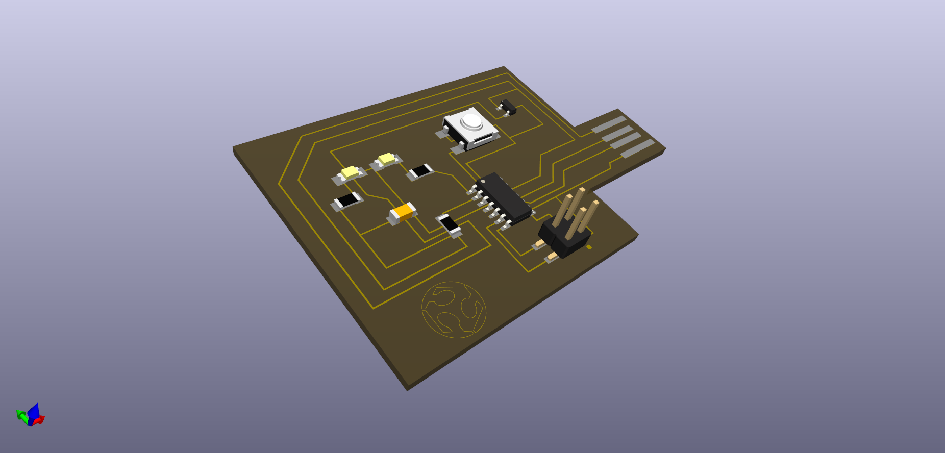
All components were placed and the traces were routed. The board outline was also defined at this stage, which is later used for the cutting process during fabrication.
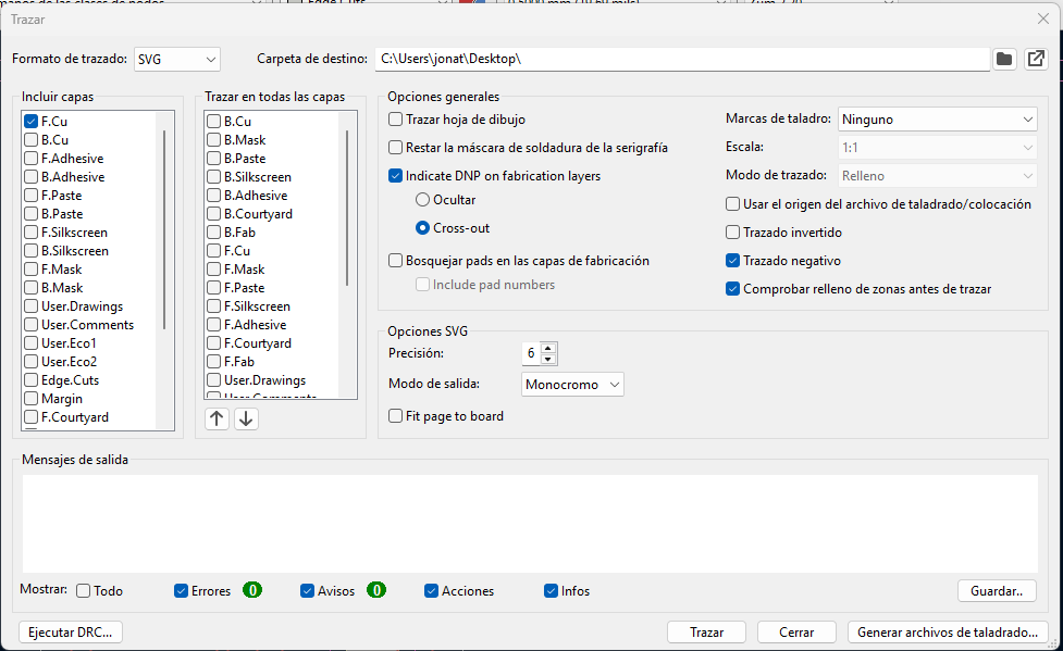
The design was exported as SVG and prepared for fabrication using Inkscape and Mods. The traces were converted into a black-and-white image to generate the toolpaths . However, this stage introduced several challenges, because High DPI values and an excessive number of offsets generated files that were too large, causing the machine to stop processing at around 30% of the job.
These issues directly affected the milling results: insufficient cutting depth prevented the complete removal of copper, while incorrect tool configurations caused burrs or lifted traces. Through this process, it became clear that PCB fabrication depends not only on having a correct design but also on properly preparing and optimizing the files and machining parameters for the milling process.
Circuit Simulation
The simulated system was developed using Circuit Simulator, where the necessary components to properly control a solenoid (Final Project) were included. However, since the solenoid component was not available in the schematic library, a 30 Ω resistor was used to represent the electrical path of the load.
The simulated circuit represents the control of a solenoid (Final Project), which functions as an electromagnetic actuator. The MOSFET is used as an electronic switch that allows the solenoid to be turned on and off through a control signal. When the MOSFET is activated, current flows from the 12 V supply to the solenoid coil, generating a magnetic field that produces the movement of the mechanism. When the MOSFET turns off, the energy stored in the coil attempts to keep the current flowing.
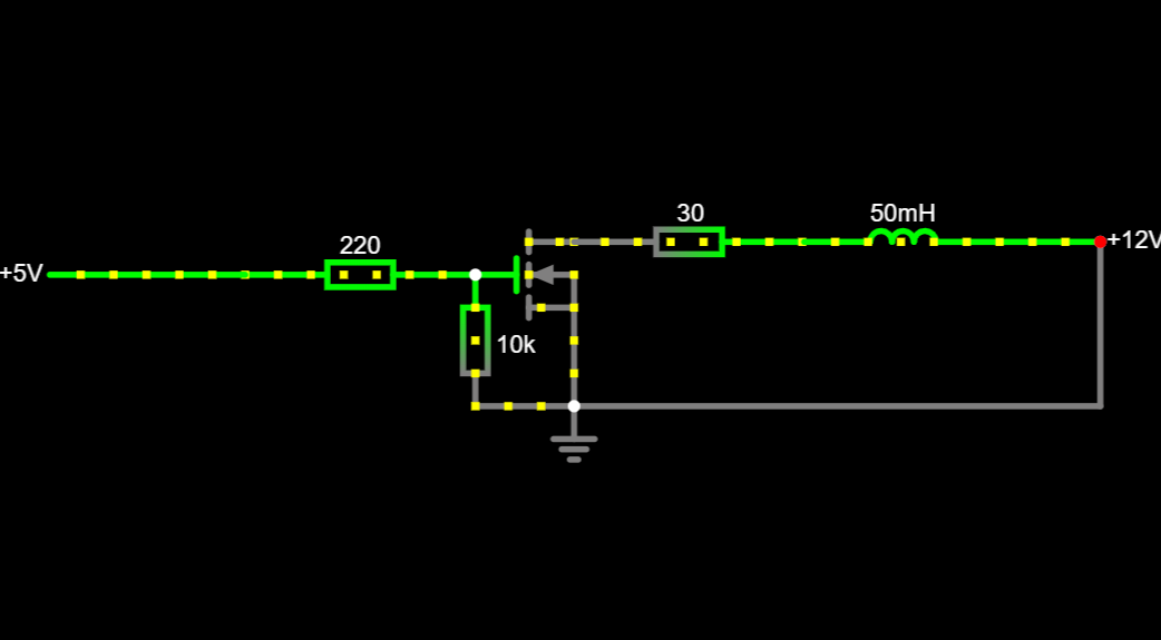
Because the solenoid is essentially a coil, the current does not appear instantaneously and part of the energy is temporarily stored in its magnetic field. To prevent voltage spikes that could damage the transistor or the microcontroller in the project, a flyback diode is used. This diode provides a safe path for the current and allows the energy stored in the solenoid coil to dissipate safely.
Characterization

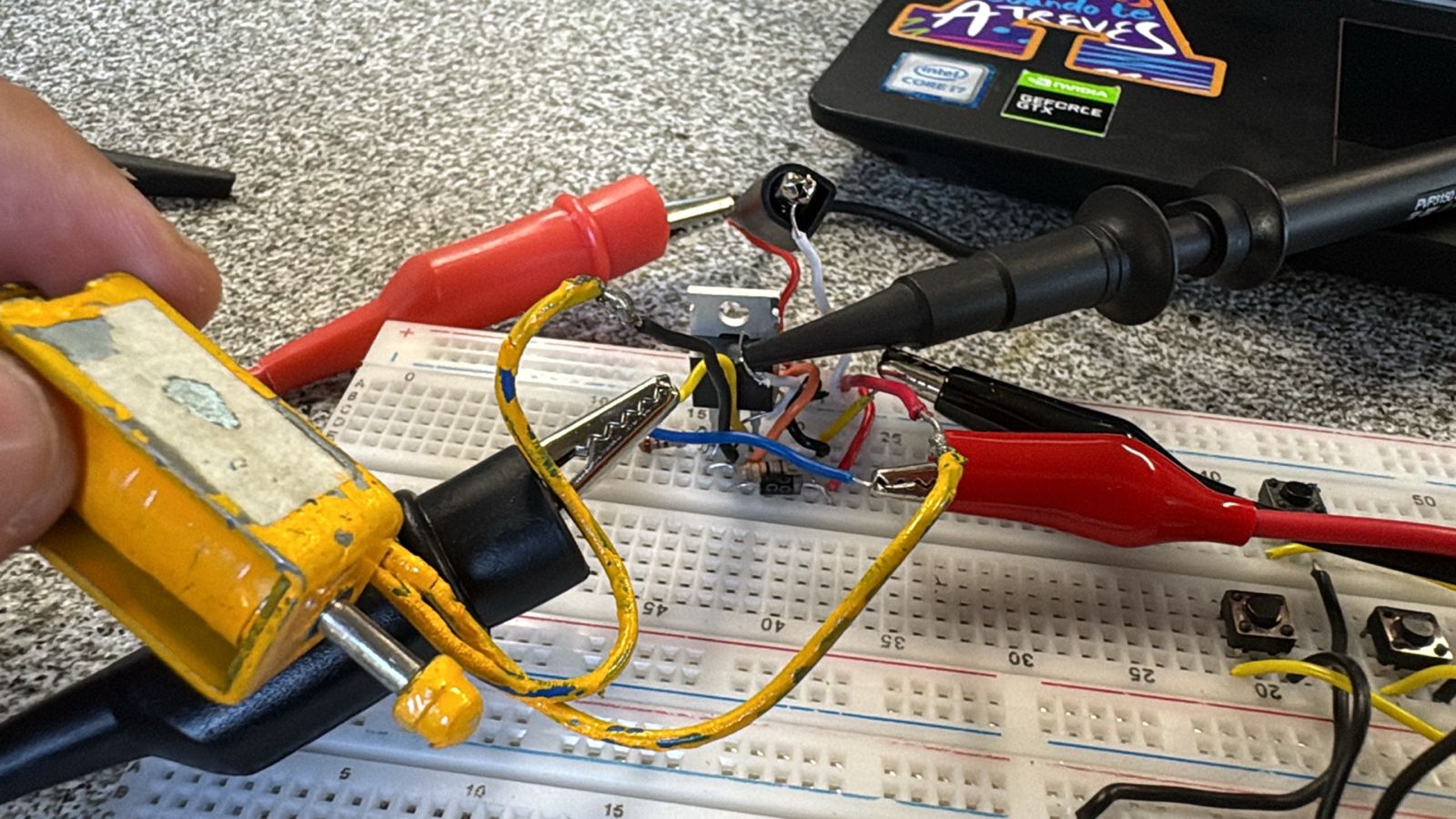
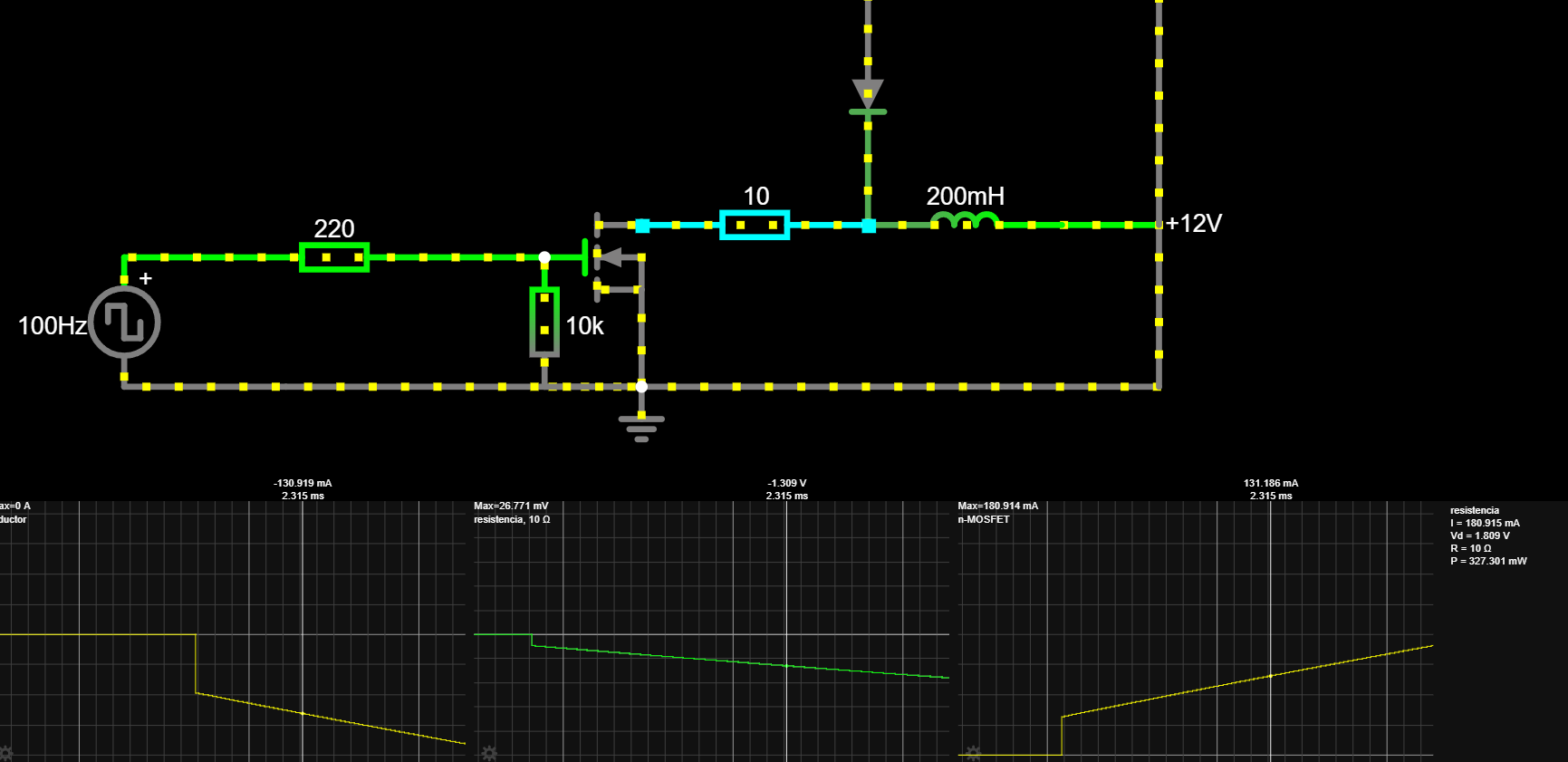
To control the solenoid, I designed a low-side driver using an n-channel MOSFET, a series gate resistor, a pull-down resistor to ground, and a flyback diode in parallel with the coil. Since the simulator did not include the exact actuator component, I first represented the load as an equivalent RL network to study the current delay and the dissipation of the energy stored in the inductance when switching it off. This model was sufficient to validate the circuit logic and the need for the protection diode to prevent voltage spikes in an inductive load.
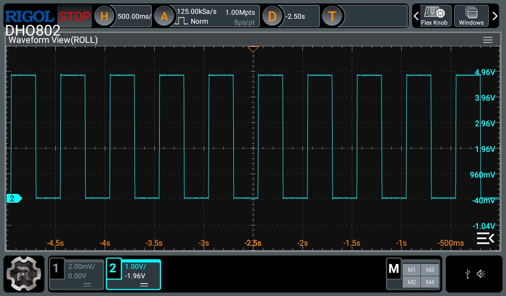
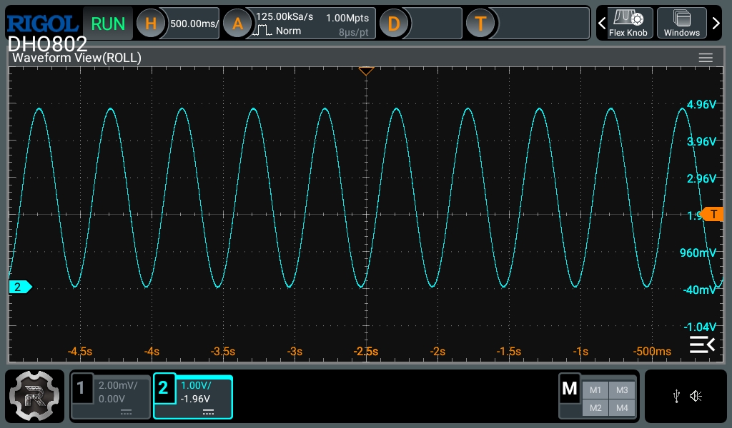
In hardware, I used a 0 to 5 V square wave to drive the gate. On the oscilloscope, I measured a gate signal of approximately 0–4.96 V and a complementary drain signal of approximately 12.20–0.10 V, which confirmed that the MOSFET was switching correctly and that the solenoid was indeed being energized. The small overshoot observed at the drain was consistent with the normal behavior of an inductive load with current recirculation. Even so, this test also showed that the final MOSFET selection must be verified using its specified RDS(on) at the actual gate-drive voltage, and not only VGS(th).