8. Electronics Production
Assignment
Group Assignment
- Characterize the design rules for the in-house PCB production process and document the machine settings.
- Document the workflow for sending a PCB to a commercial board house.
- Document the group work on the group assignment page and reflect on the learning outcomes on the individual page.
Individual Assignment
- Design, manufacture, and test a custom microcontroller development board.
Learning Outcomes
By completing this assignment I learned to:
- Describe the complete PCB production workflow, including:
- Toolpath generation
- PCB milling
- Soldering components
- Debugging hardware
- Programming the microcontroller
- Demonstrate an effective PCB fabrication workflow while identifying areas for future improvement.
Overview of the PCB Production Process
The overall PCB fabrication workflow consists of the following stages:
- Design the schematic and PCB layout.
- Export the PCB layout.
- Prepare the milling layers.
- Generate toolpaths using MODs.
- Mill the PCB.
- Solder the electronic components.
- Validate and troubleshoot the completed board.
Assignments
Group Assignment: Link to group page
Individual Assignment: PCB Layout Examples
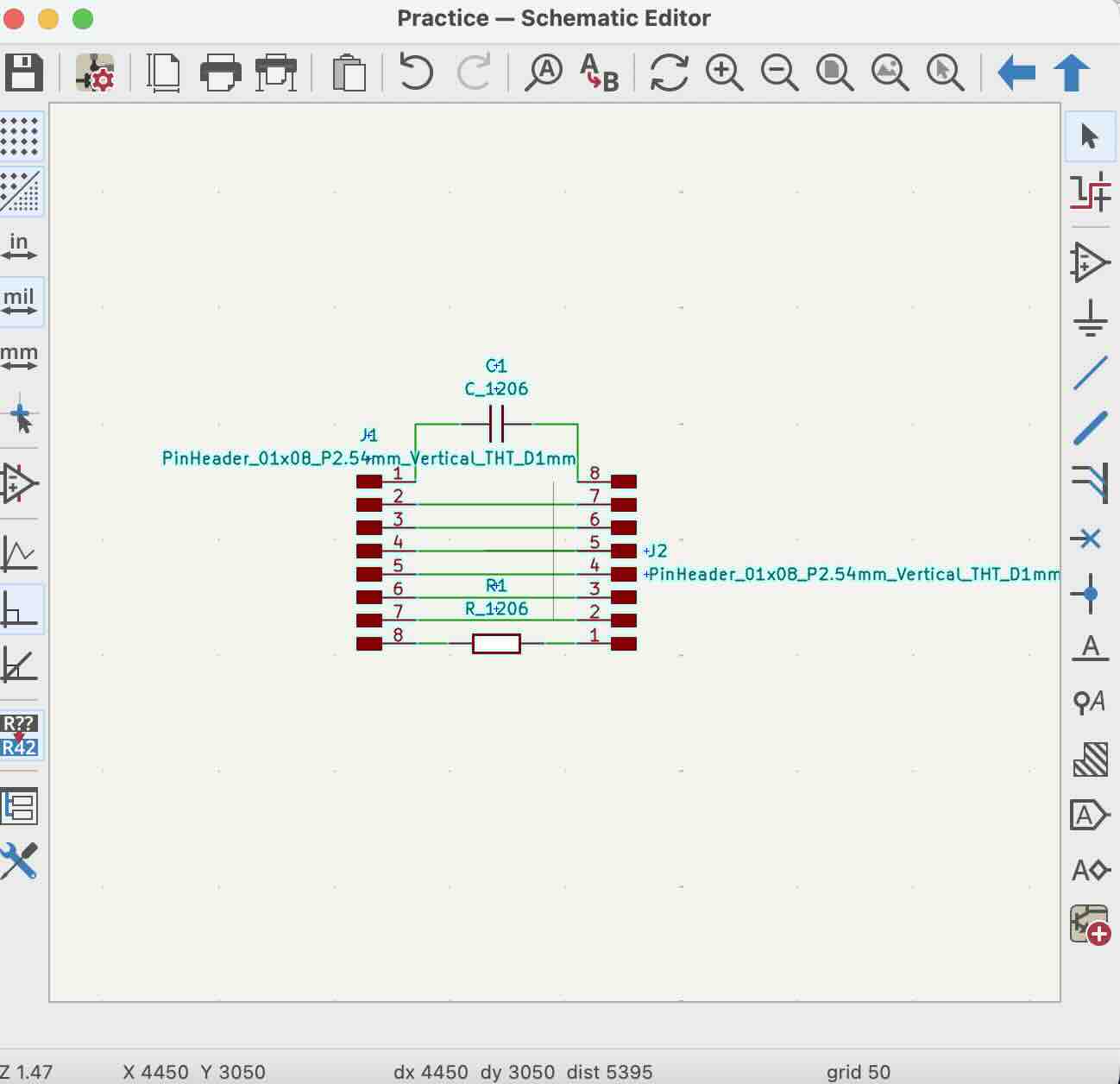
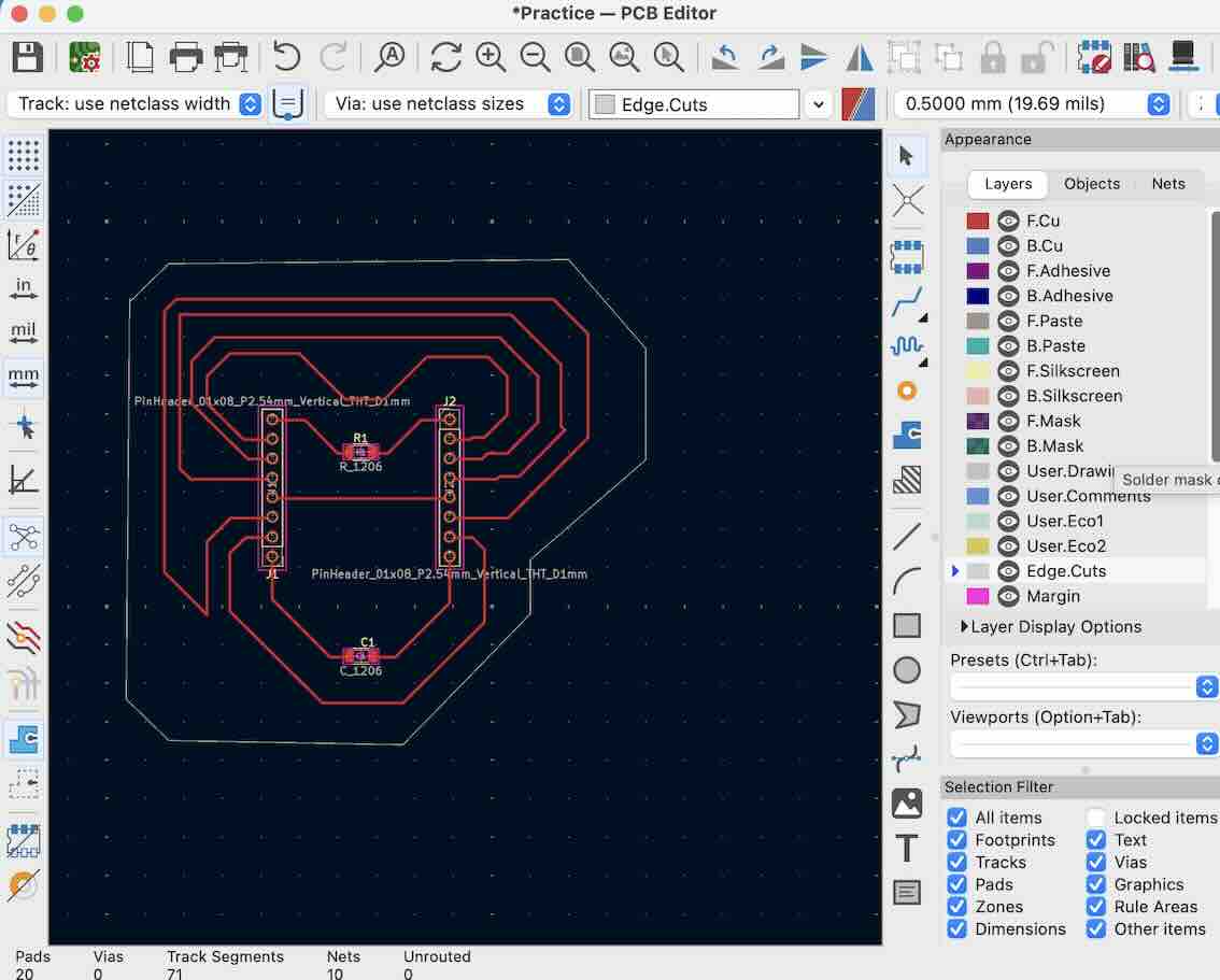
Before producing my final PCB, I practiced the export and layer preparation workflow using a very simple demonstration board.
The example consists of:
- Two pin headers
- One capacitor
- One resistor
Using this simplified design made it much easier to understand the export process before moving on to a more complex PCB.
Exporting the PCB Layout
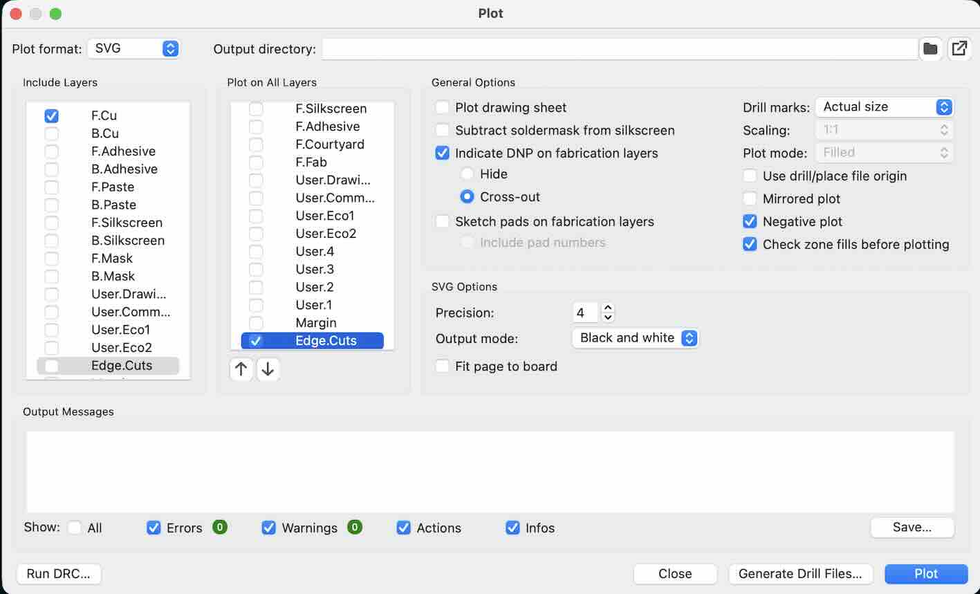
Once the PCB design is complete, export it as an SVG file.
Only export:
- Copper trace layers
- Edge Cuts layer
Navigate to:
File → Plot → Save as SVG
After exporting, KiCad should display a confirmation message indicating that the selected layers were successfully plotted.
Preparing the SVG in Inkscape
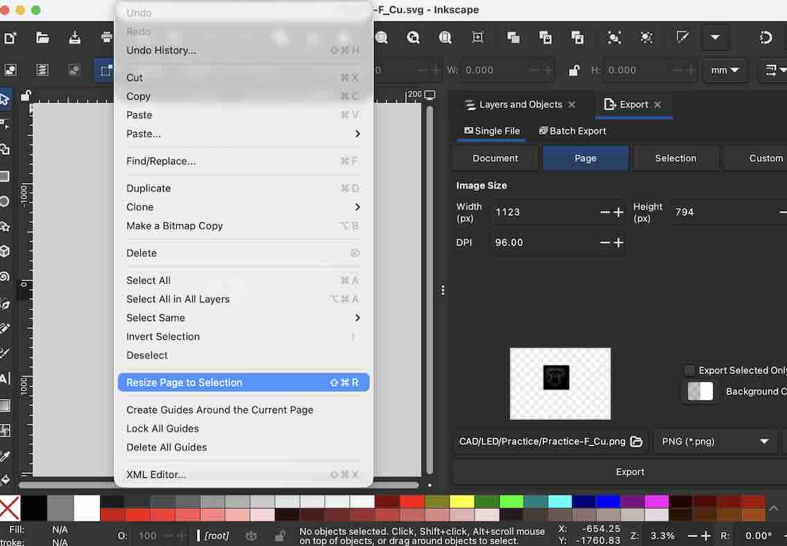
Open the exported SVG file in Inkscape.
Once opened:
- Resize the page to fit the selected objects.
Separate the PCB Layers
Separate the drawing into the individual layers that will be milled independently.
Typical layers include:
- Traces
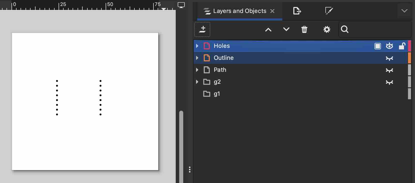
- Holes
- Board Outline
Move each group of vectors onto its own layer.
Important
For PCB milling:
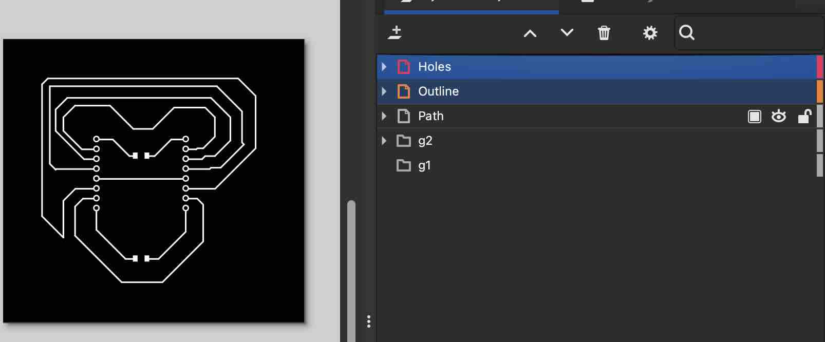
- White represents the material that will remain.
- Black represents the material that will be removed.
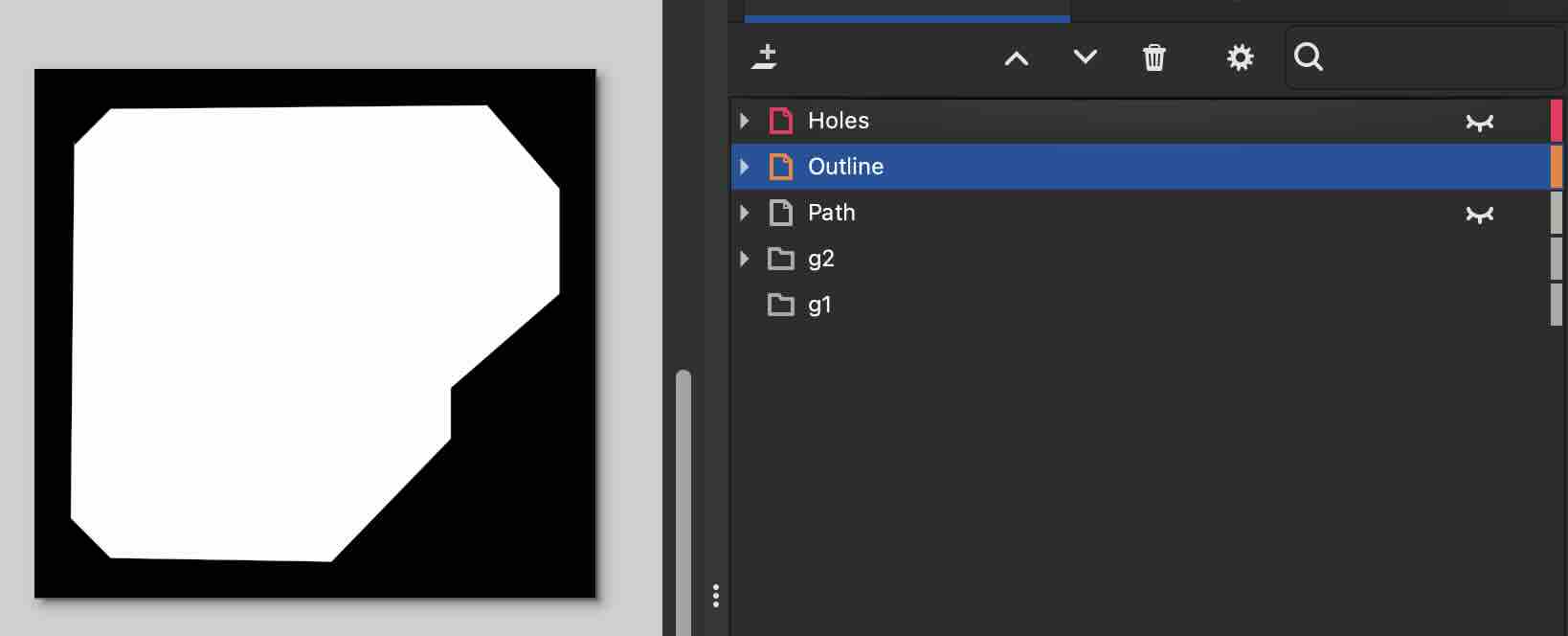
For the Board Outline, it is often necessary to:
- Select the outline path.
- Apply a solid fill so that the outline becomes a filled shape rather than a thin stroke.
Trace Layer
Hole Layer
Board Outline
Exporting Each Layer
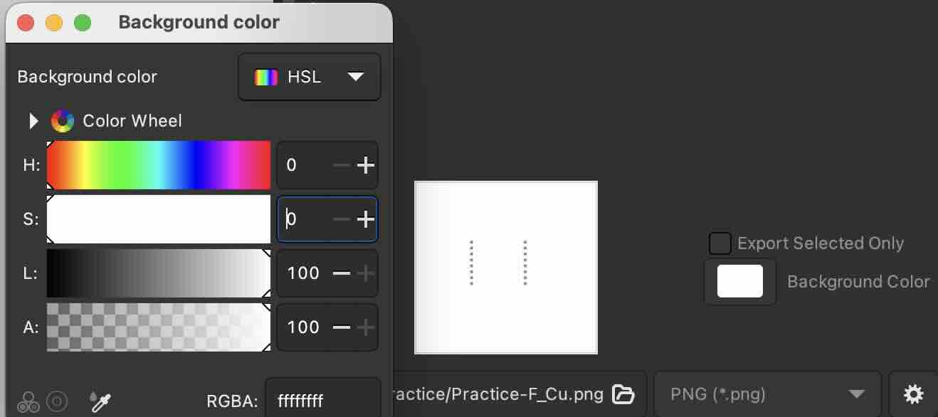
Each PCB layer must now be exported individually.
For every layer:
- Export as PNG
- Set the resolution to 1000 DPI
- Ensure the background is white
- Make sure nothing is selected before exporting
Generating Toolpaths with MODs
A detailed step-by-step guide for using MODs can be found here:
https://fabacademy.org/2019/docs/FabAcademy-Tutorials/week04_electronic_production/mods.html
Note: The following workflow was completed using my final PCB rather than the simple demonstration board shown previously.
Opening MODs
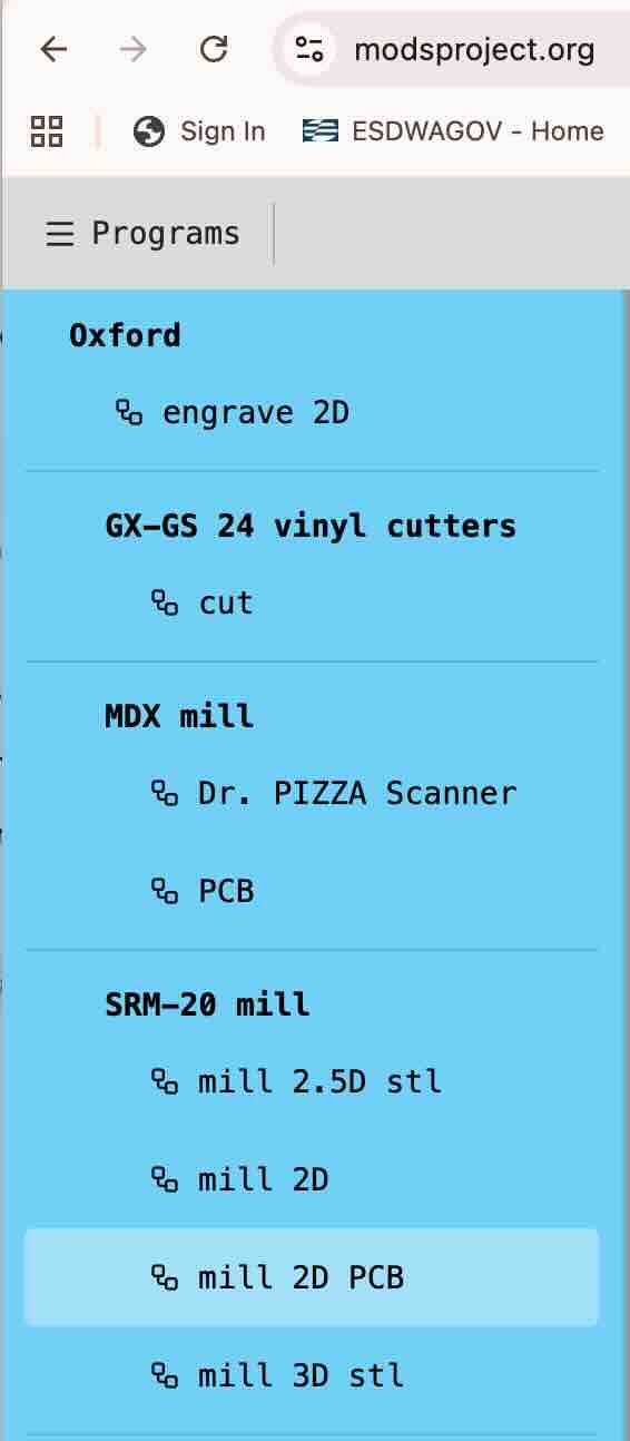
- Navigate to https://modsproject.org/
- Select:
Programs → Open Program → Roland → SRM-20 PCB
Load the PNG File
Use the Select PNG module to load the layer that will be machined.
Each PCB layer requires its own MODs program and toolpath.
The machining order should always be:
- Traces
- Holes
- Board Outline
Configure the Tool Settings
Adjust the machining settings for the selected layer.
Trace Layer
Several preset trace options are available.
If using a V-bit, use the built-in V-Bit Calculator.
The calculator automatically overrides the default PCB settings based on the entered tool geometry.
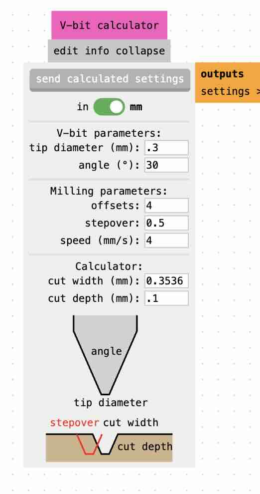
Adjust any remaining machining inputs as required.
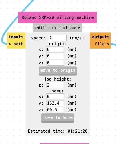
Simulate the Toolpath
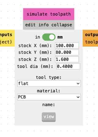
Before generating the machining file, simulate the toolpath.
This allows any issues to be identified before milling.
Things to verify include:
- Correct tool selection
- Correct cutting depth
- Complete trace isolation
- Proper board outline
Save the Toolpath
Once the simulation looks correct:
- Save the generated machining file.
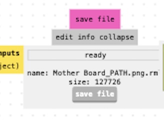
Repeat this process for each PCB layer.
For the Drill and Board Outline operations, use the standard PCB preset settings supplied with MODs.
Common Issue
Holes Do Not Appear
Occasionally the drill holes may not appear correctly after importing the SVG.
Cause
The exported geometry has been scaled incorrectly in Inkscape.
Solution
Return to Inkscape and verify that the objects have been scaled correctly before exporting the PNG again.
PCB Milling
After generating all of the toolpaths, the PCB can be machined.
The PCB stock consists of a rigid plastic substrate coated with a thin layer of copper.
Preparing the Material
-
Transfer the machining files to the dedicated PCB milling computer using a USB flash drive.
-
Secure the PCB blank to the machine bed using double-sided tape.
Tape Placement
- Use a single continuous layer of tape covering most of the back of the PCB.
- Ensure the board is completely flat against the bed.
Even very small areas that lift away from the machine bed can significantly affect the milling depth and ruin the PCB.
Setting the Machine Zero
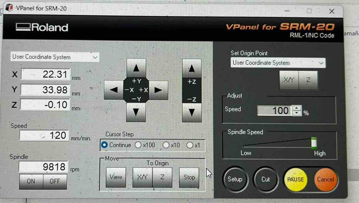
Open the Roland milling software.
Set the X and Y Zero
- Use the movement controls to position the tool at one corner of the PCB material.
- Set both the X and Y origins.
Set the Z Zero
Move the tool slightly inward from the corner.
Lower the cutter until it is very close to the PCB surface.
Then:
- Loosen the collet.
- Allow the cutter to gently fall until it just touches the surface.
- Tighten the collet again.
This provides an accurate Z reference without applying unnecessary force to the cutter.
Milling Order
Run the machining programs in the following order:
- Traces
- Holes
- Board Outline
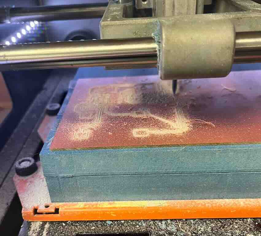
Finished PCB
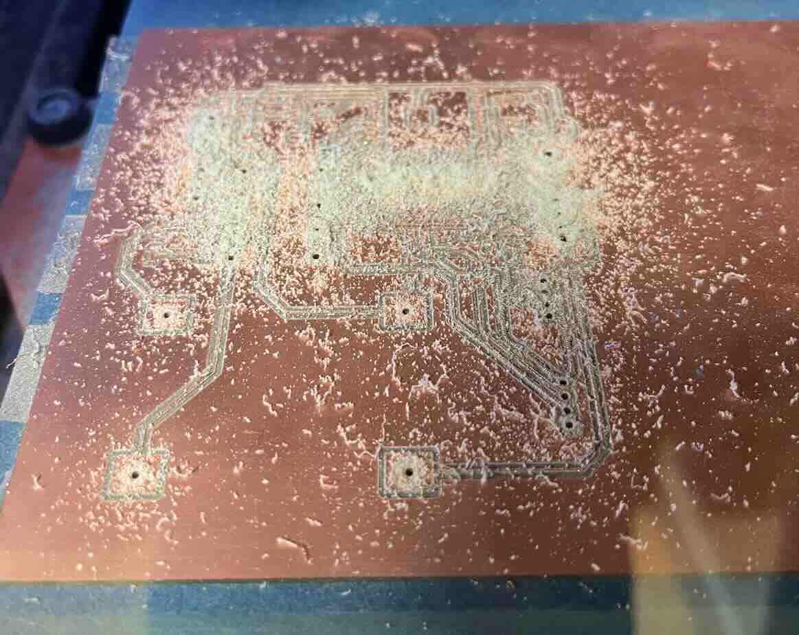
The final machining operation cuts the board outline, releasing the PCB from the stock material.
Once machining is complete:
- Remove the board from the machine.
- Lightly polish the surface using steel wool or very fine sandpaper.
This helps to:
- Remove burrs
- Clean the copper traces
- Improve solderability
- Produce a cleaner finished PCB
Soldering
Once the PCB has been milled and cleaned, the next step is soldering the electronic components to the board.
Soldering creates electrically conductive connections between the components and the copper traces that were milled in the previous step.
Setting Up a Soldering Station
Before beginning, prepare a clean and organized workspace.
Gather all required components and equipment:
- Electronic components
- Soldering iron
- Solder wire
- Wet cleaning sponge
- Tweezers
- Good lighting
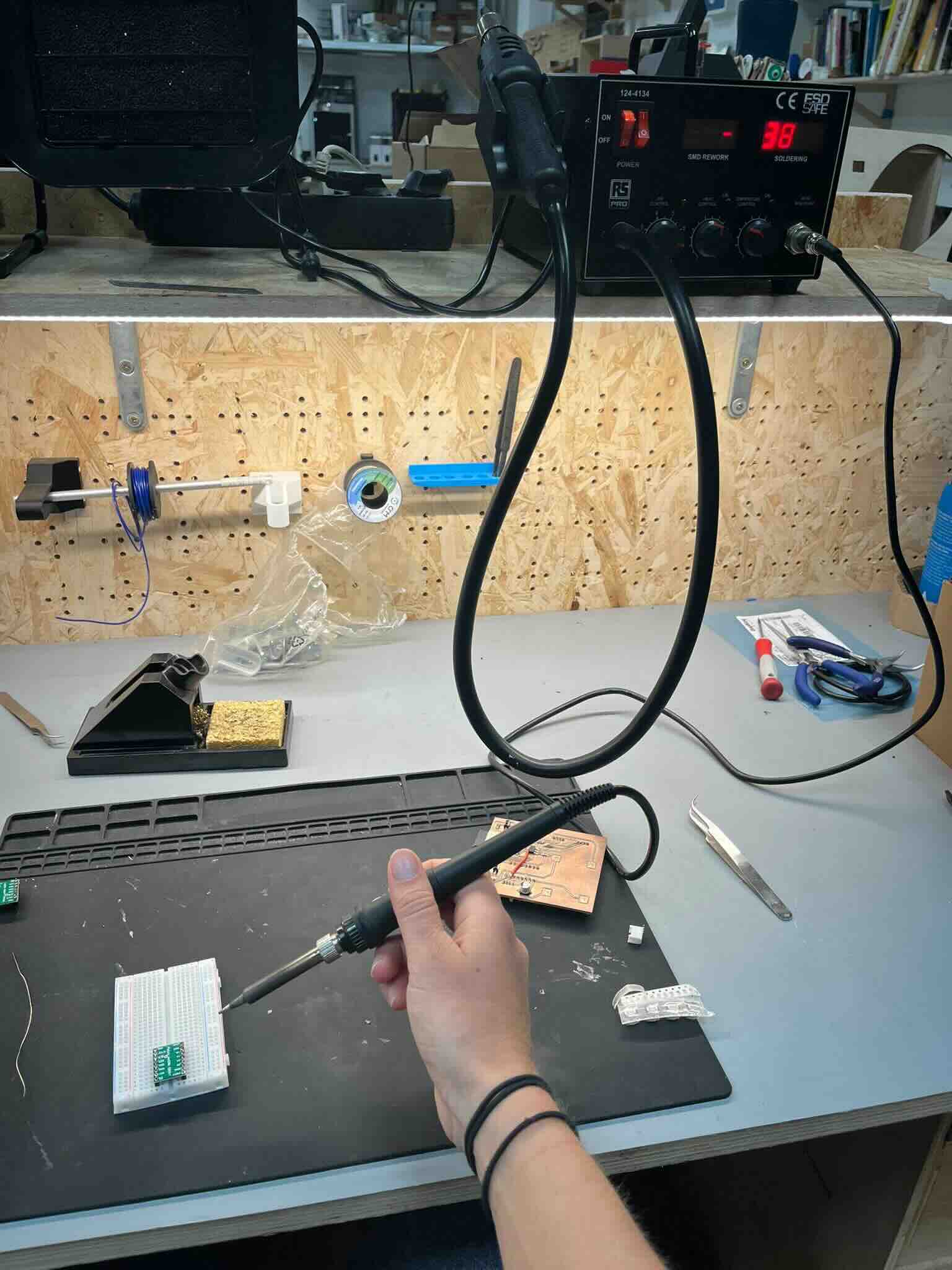
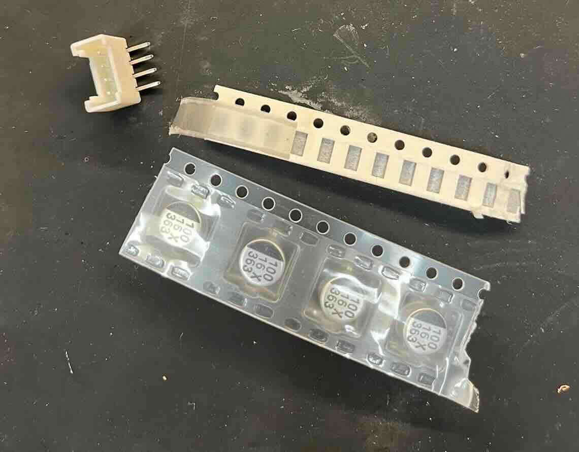
Components
Collect all of the components required for the PCB before beginning assembly.
Having everything organized beforehand makes the soldering process much smoother.
Installing Breakout Boards
This project uses several breakout boards connected to the custom PCB through pin headers.
Using breakout boards is an excellent way to practice soldering because the headers are relatively easy to align and inspect.
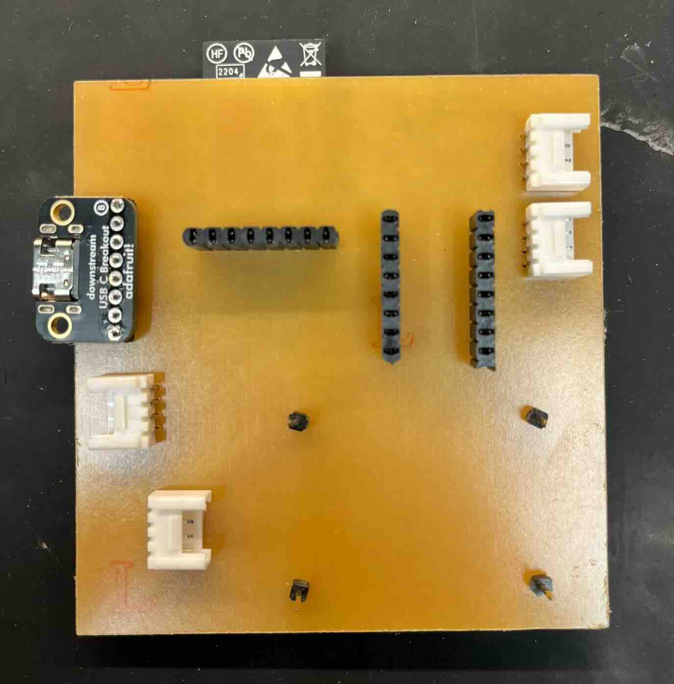
The pin headers are soldered from the back of the PCB while the breakout boards are mounted on the front.
Positioning the Components
Before applying heat, ensure the components are held securely so they cannot move during soldering.
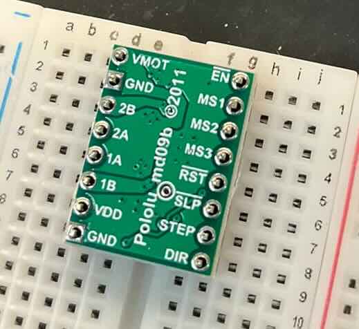
A breadboard is particularly useful when soldering pin headers because it keeps the pins perfectly aligned.
The image below shows a breakout board positioned on a breadboard, ready to be soldered.
Proper Soldering Technique
A good solder joint is formed by heating both pieces being connected rather than melting solder directly onto the iron.
Position the soldering iron so that it simultaneously contacts:
- The PCB pad
- The component lead or pin
This heats both surfaces evenly.
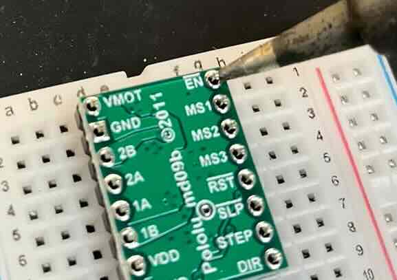
Once both parts have reached soldering temperature:
- Feed a small amount of solder into the joint (not directly onto the iron).
- Allow the solder to flow naturally around both surfaces.
- Remove the solder wire first.
- Remove the soldering iron after the joint has fully wetted.
The finished joint should appear smooth, shiny, and slightly concave.
Installing the Remaining Components
After the pin headers have been installed, continue soldering the remaining components one at a time.
For each component:
- Position the component accurately.
- Heat both the pad and the component lead simultaneously.
- Apply a small amount of solder.
- Allow the joint to cool before moving to the next connection.
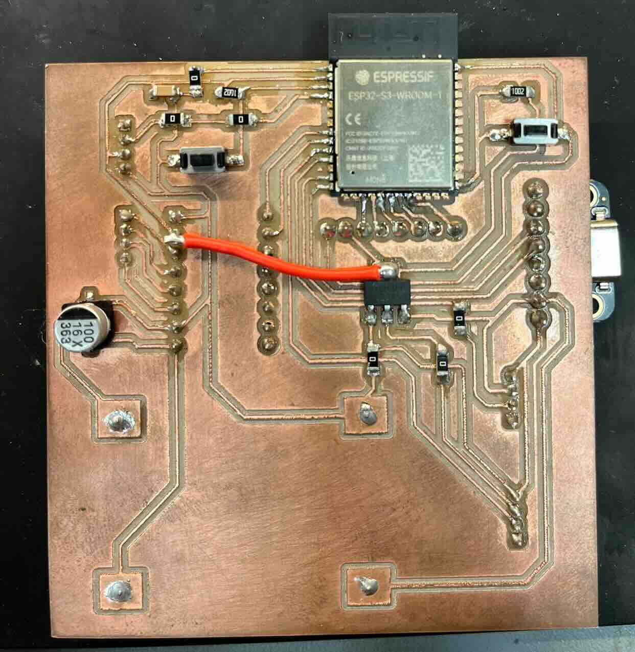
In this project, the breakout boards were mounted on the front of the PCB while the pin headers were soldered on the back.
This configuration reduces the mechanical stress placed on the PCB traces when breakout boards are repeatedly installed and removed.
Validation and Troubleshooting
It is uncommon for a newly manufactured PCB to function perfectly on the first attempt.
Instead of assuming the entire design is incorrect, it is much more effective to validate the board systematically by checking one subsystem at a time.
The validation process I followed consisted of:
- Power verification
- Continuity testing
- Programming the microcontroller
- Testing each peripheral individually
Testing with Continuity
The first step was confirming that the PCB was receiving power correctly.
After powering the board, I measured the voltage supplied to the ESP32 and discovered that only one of the 3.3 V pins was connected.
Reviewing the schematic revealed that a connection had been accidentally omitted during PCB design.
After correcting this issue, I performed continuity testing across the remainder of the board.
The continuity checks included:
- Ground connections
- Power rails
- Pin headers
- Signal traces
- Component connections
Once every trace showed proper continuity, the board was ready for functional testing.
Testing with Programming
After verifying the hardware, I tested each peripheral individually by gradually expanding the program.
My PCB contained four input/output devices:
- LED
- PIR motion sensor
- Stepper motor
- Push-button switch
Step 1 — LED
The first test simply blinked the onboard LED.
This confirmed that:
- The microcontroller was functioning.
- Programming was successful.
- The LED circuitry worked correctly.
Step 2 — PIR Motion Sensor
Next, I connected the PIR sensor.
The program was modified so that the LED illuminated whenever motion was detected.
This verified both:
- The PIR sensor
- The GPIO interface
Step 3 — Motor and Switch
Finally, the remaining devices were added one at a time.
After each new component was connected:
- The firmware was updated.
- The new functionality was tested before continuing.
Testing each subsystem independently made it much easier to identify faults if they occurred.
Issues Discovered During Validation
Systematically testing each subsystem helped isolate two hardware issues that prevented the board from operating correctly.
Issue 1 — Missing 3.3 V Connection
Symptoms
- The ESP32 did not receive power.
- The board could not be programmed.
- The microcontroller was not detected by the Arduino IDE.
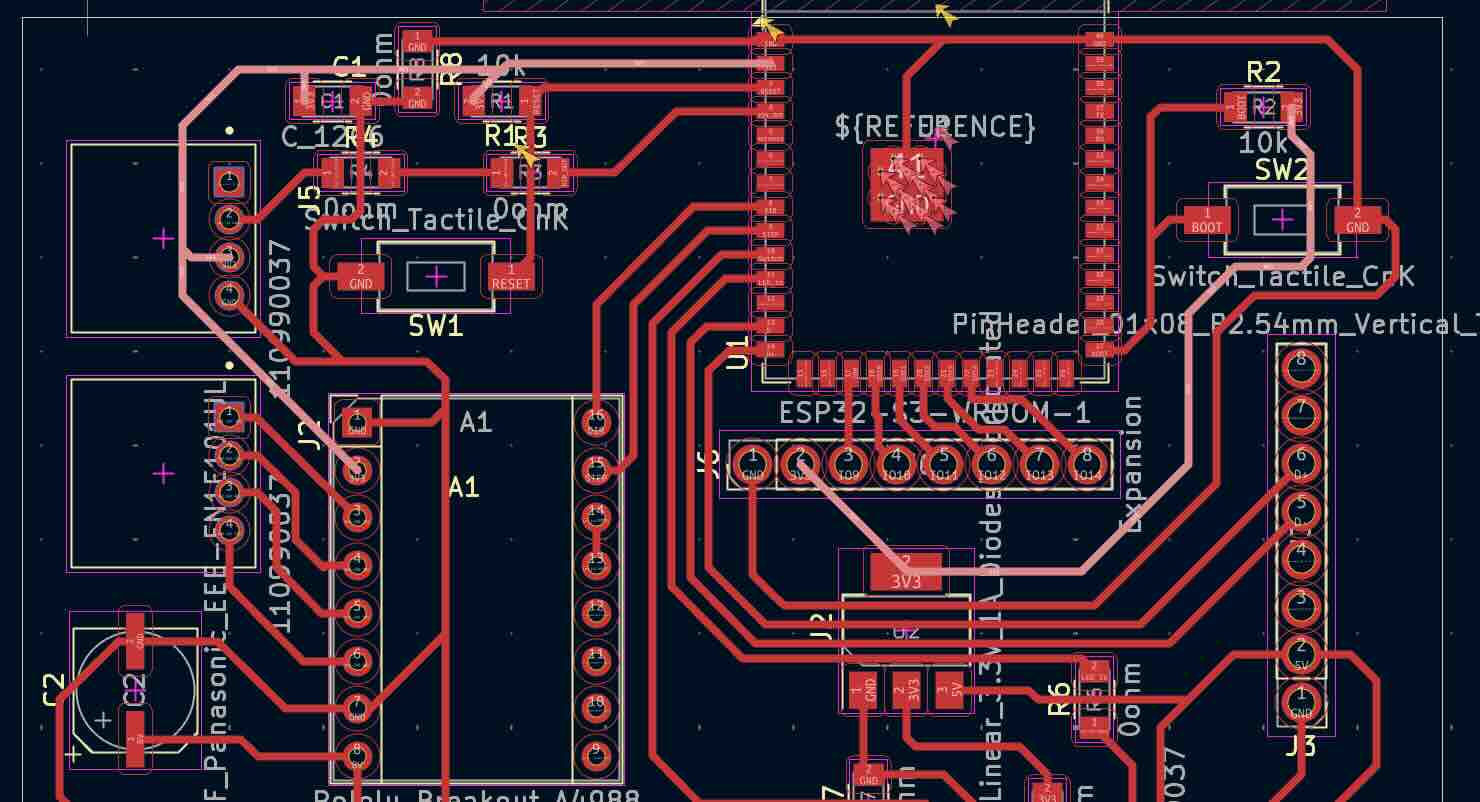
Cause
While reviewing the schematic after measuring the voltage rails, I discovered that one of the required 3.3 V connections had been omitted during PCB routing.
As a result, only one of the ESP32’s three 3.3 V pins was connected, preventing the microcontroller from operating correctly.
Solution
A jumper wire was added to restore the missing connection.
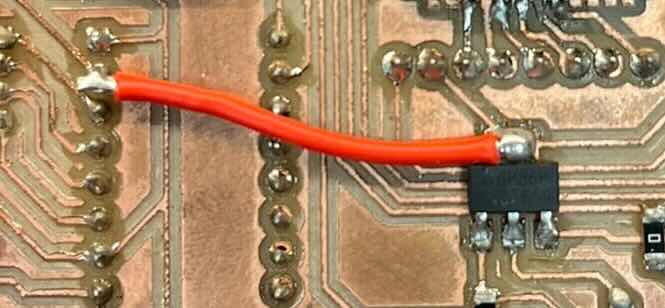
After adding the jumper, the ESP32 powered up correctly and could be programmed normally.
Issue 2 — Reset Pull-up Connection
Symptoms
- The board frequently disconnected from the Arduino IDE.
- Uploading programs often failed.
- The board appeared to reset unexpectedly during programming.
- After successful uploads, the board would briefly lose power before restarting, making it appear as though the connected inputs and outputs were malfunctioning.
Cause
The problem was traced to an unreliable connection on the reset pull-up resistor.
Because the reset line was unstable, the ESP32 repeatedly entered the reset state, interrupting communication with the programmer.
Solution
After repairing the faulty pull-up connection, the board became stable.
Programming completed reliably, and the peripherals behaved as expected during testing.
Reflection
Designing and manufacturing a custom PCB provided valuable insight into every stage of the electronics production workflow. Rather than simply assembling an existing design, I was responsible for the complete process, including PCB layout, preparing manufacturing files, milling the board, soldering the components, and validating the finished hardware.
One of the biggest lessons from this assignment was the importance of systematic debugging. Rather than assuming the entire board was faulty, testing each subsystem independently allowed problems to be isolated quickly. Beginning with power distribution, then checking continuity, followed by programming and finally validating each peripheral one at a time, made troubleshooting far more manageable.
The assignment also reinforced how small mistakes made during the design stage can have significant consequences during fabrication. Missing a single routed connection or overlooking a pull-up resistor resulted in hardware failures that required careful investigation to identify. Performing electrical checks before attempting to debug software saved considerable time.
Overall, this assignment significantly improved my understanding of PCB design, fabrication, soldering, and hardware debugging, and gave me confidence in developing custom embedded electronics from initial schematic through to a fully functioning prototype.