6. Electronic Design
Objectives of the Week
-
Select and use software for circuit board design
-
Demonstrate workflows used in circuit board design
Schedule
Wednesday, Feb 25 - [Global Class - Electronic Design][]
Thursday, Feb 26: - Electronic Design
Friday, Feb 27: - Electronic Design
Assignments
Group assignment:
-
Use the test equipment in your lab to observe the operation of a microcontroller circuit board (as a minimum, you should demonstrate the use of a logic analyzer)
-
Document your work on the group work page and reflect what you learned on your individual page
Individual assignment:
- Use an EDA tool to design a development board that uses parts from the inventory to interact and communicate with an embedded microcontroller
Class Notes
Thursday - Basics of Electronics
Circuits
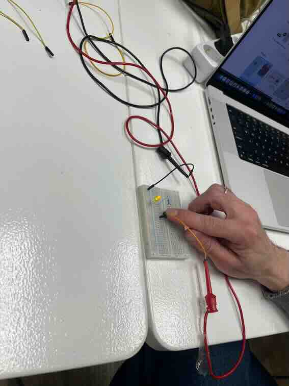
Continuity Mode - Used to test the connection across components or a circuit
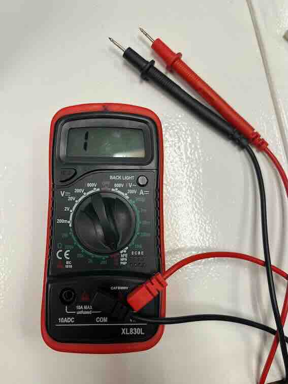
Measuring Voltage - Turn the multimeter dial to V with the straight line (DC voltage)
Measured Values
-
AD: 4.96 V
-
AB (across resistor): 2.28 V
-
BD (across LED): 2.64 V
Measuring Tools
Multimeters
-
Measures values instantaneously
-
Example shown above
-
Cannot measure signals that change very quickly (ex: PWM)
Oscilloscope
-
Records signal behavior over time
-
Can change:
-
Vertical axis → voltage scale
-
Horizontal axis → time scale
-
-
Allows you to observe electrical potential differences over time
-
Useful for observing signal bounce during startup
-
Set a trigger so recording begins when the signal starts
-
Often recorded at very small time frames (milliseconds)
-
Communication Lines
SCL
- Clock signal
SDA
- Data signal
Friday - Designing a Board
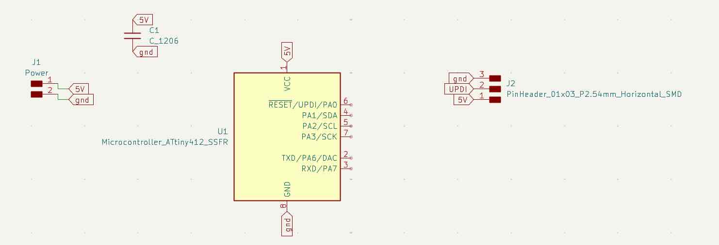
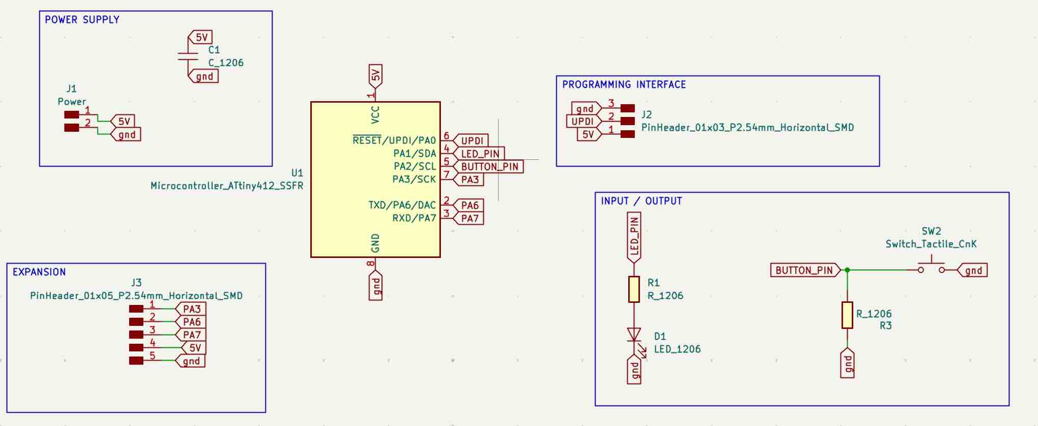
Elements to Include
-
MCU (Microcontroller Unit)
-
Power supply
-
Programming interface
-
I/O (inputs / outputs)
-
Extras
- Expose extra pins so additional components can be added later
Board Design
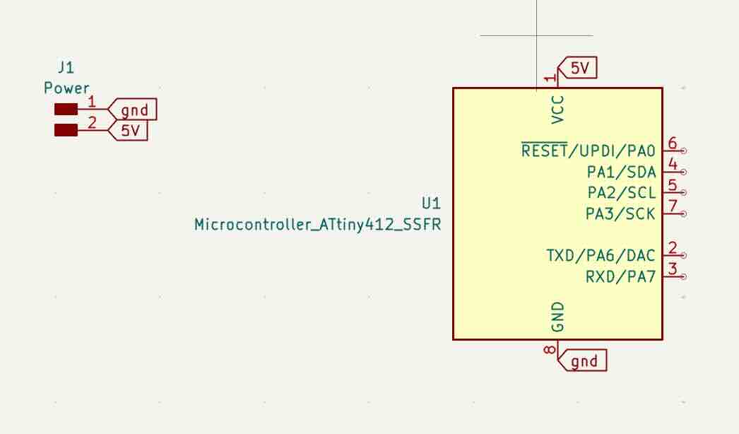
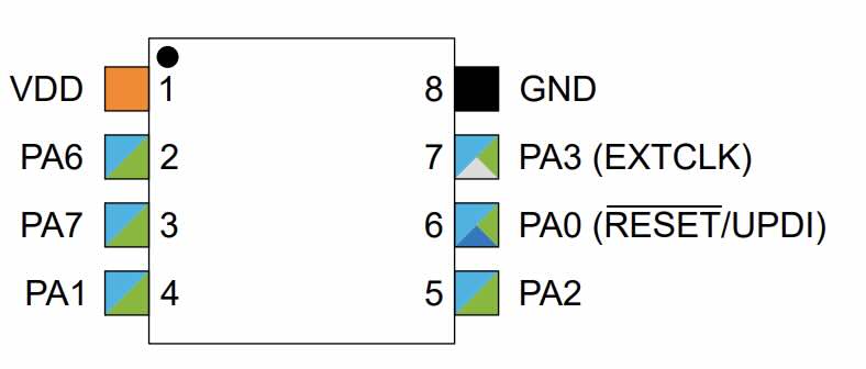
- Ensure that pins match between the schematic and the board diagram
Adding a Capacitor
-
A capacitor is needed to prevent the chip from resetting due to power instability
-
Helps stabilize voltage when the chip changes operating states
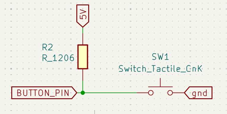
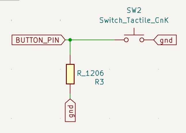
Button Circuit
-
A pull-up or pull-down resistor is required
-
This ensures current flows regardless of whether the button is pressed
-
Allows the microcontroller to detect when the button is pressed while keeping the circuit stable
- Pull-Up Resistor
- Pull-Down Resistor
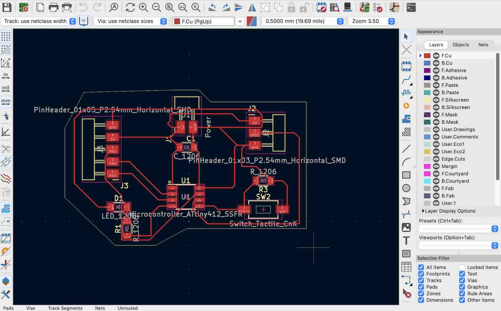
Final Board
PCB Design Workflow
-
Switch to PCB Editor (upper right corner)
-
Update schematic → PCB editor
PCB Editor
After completing the schematic, switch to the PCB Editor to begin designing the physical layout of the printed circuit board.
Import the Schematic
In the upper-right corner of KiCad, open the PCB Editor.
Update the PCB from the schematic to import all of the component footprints into the board layout.
Before proceeding, verify that every component in the schematic has a valid footprint assigned.
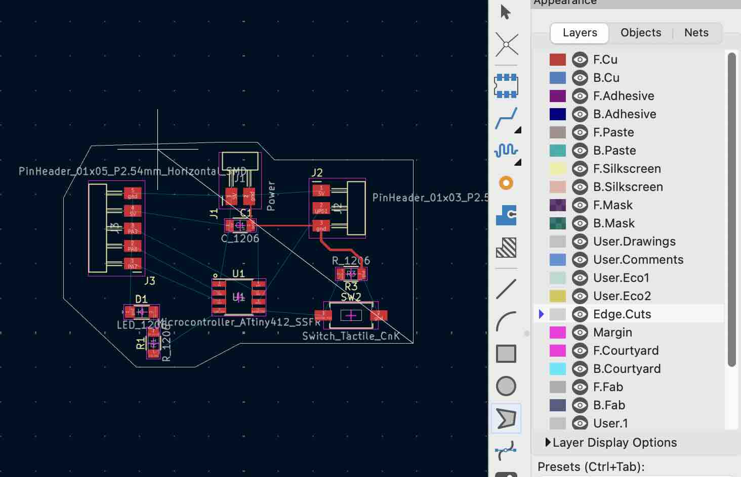
Create the Board Outline
Select the Edge Cuts layer from the layer panel on the right side of the screen.
Using the drawing tools, create the outline of the PCB.
Depending on the desired board shape, you can use:
- Polygon
- Rectangle
- Circle
Position the Components
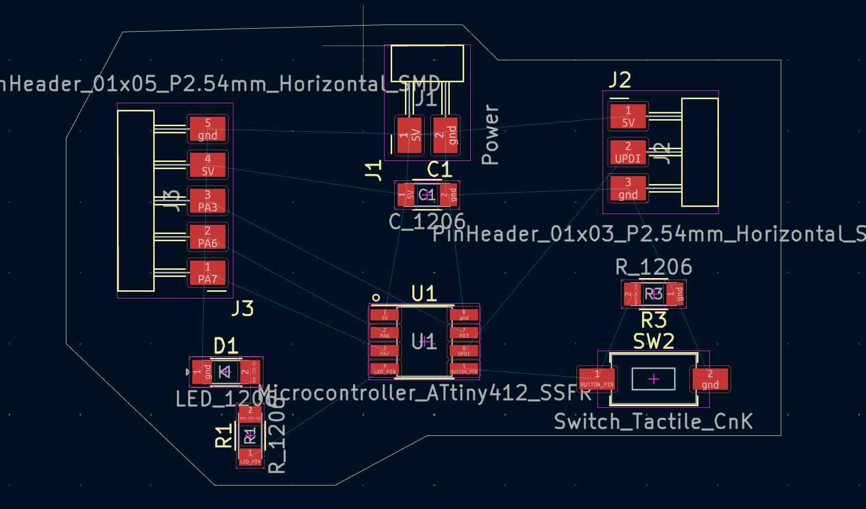
Using the selection tool, arrange the components within the board outline.
When positioning components:
- Place components with multiple interconnections close together.
- Leave sufficient space for routing.
- Consider the final placement of connectors and external components.
Good component placement greatly simplifies the routing process.
Understanding Connection Nodes
Components that need to be electrically connected are linked by thin guide lines (often called the ratsnest).
These lines indicate which pads must eventually be connected by copper traces.
Routing the Board
Select the Route Tracks tool from the toolbar.
Use it to connect the required nodes with copper traces.
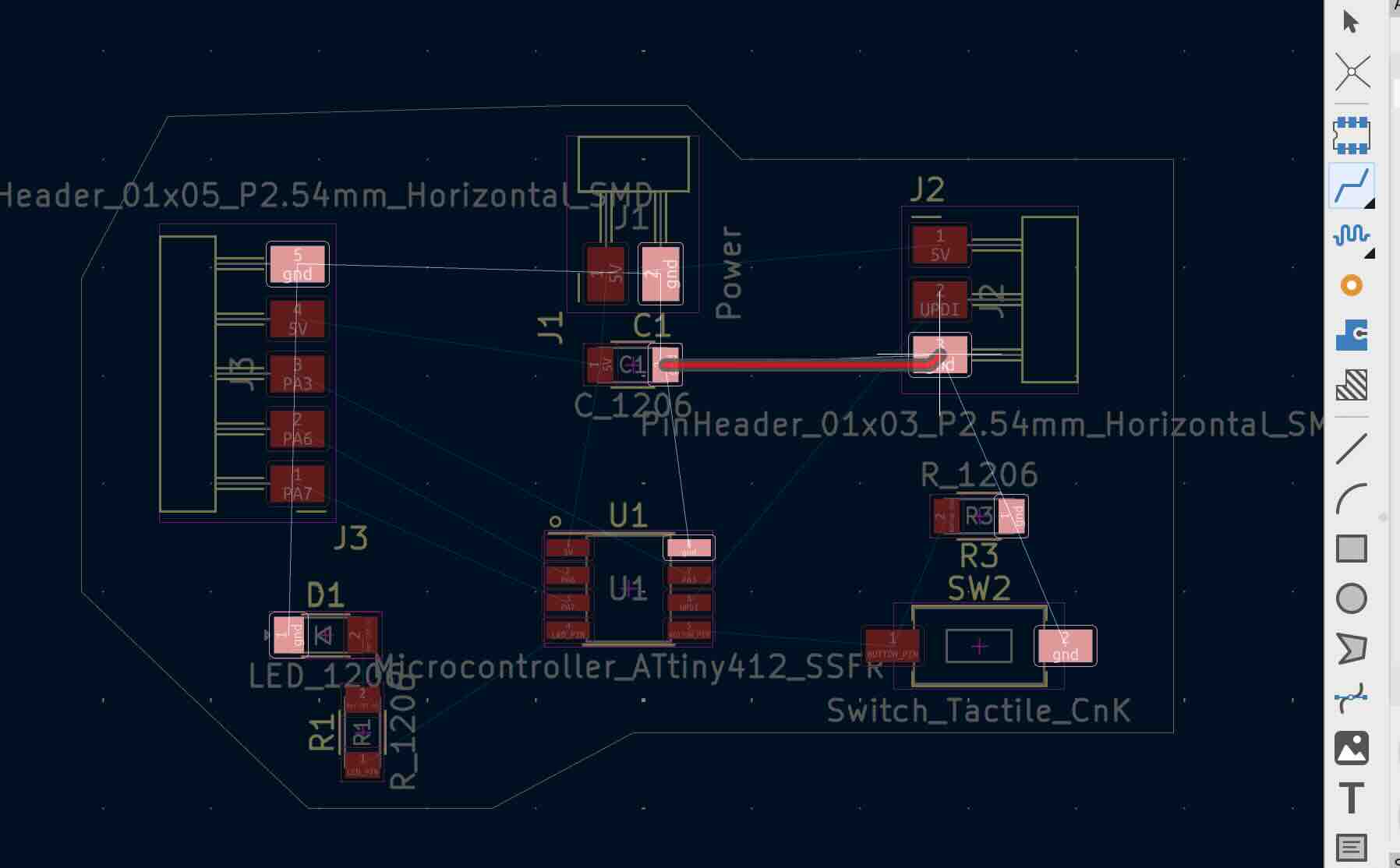
Continue routing until all required connections have been completed and the ratsnest lines disappear.
Best Practices for Routing
Track Width
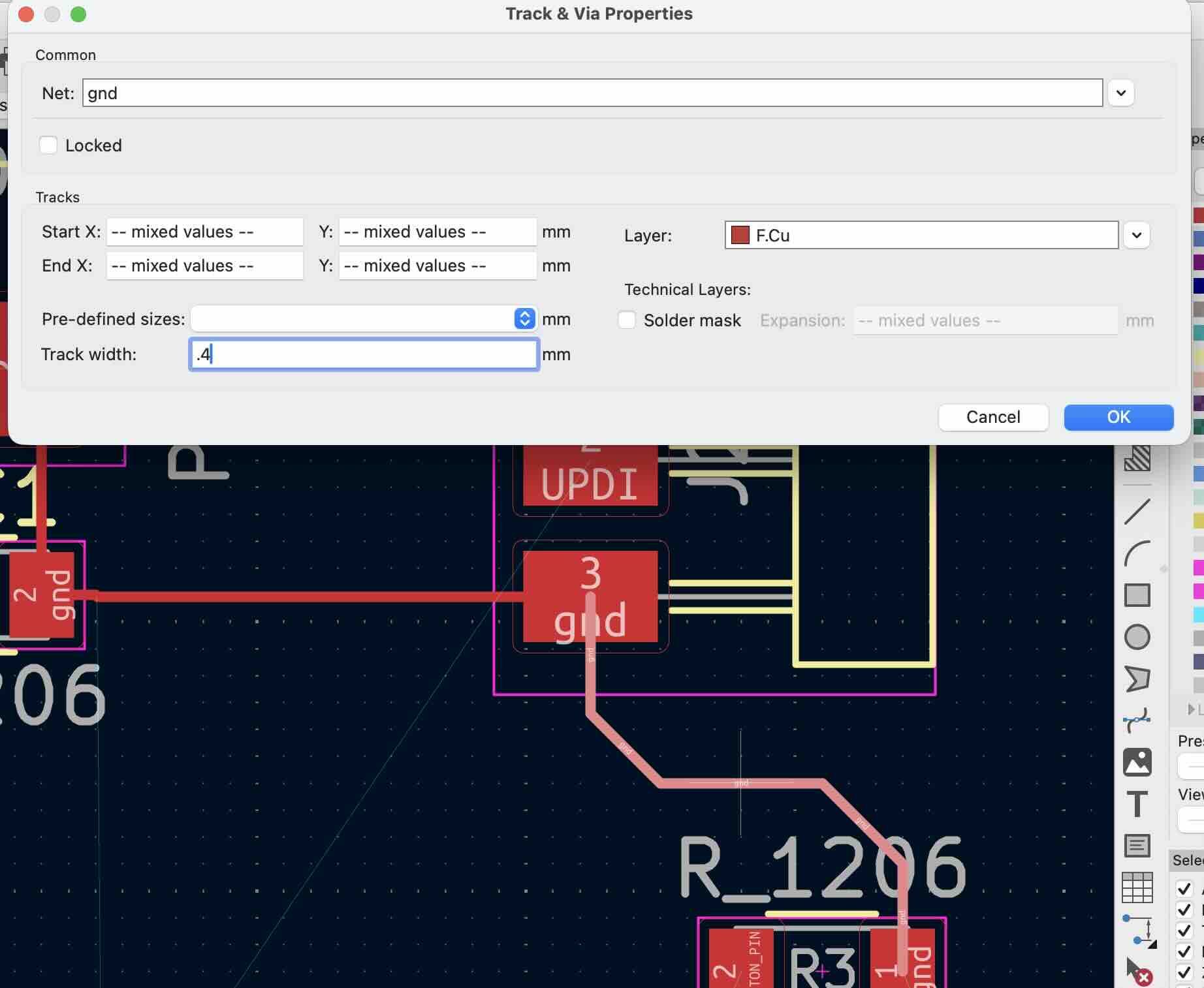
When manufacturing PCBs using an in-house milling process, wider traces are generally easier to machine and more reliable.
As a general guideline:
- A track width of 0.4 mm is a good starting point when space permits.
Editing Track Width
To modify an existing trace:
- Press U to select all connected track segments.
- Click the selected trace again to open the Track Properties window.
- Adjust the track width as required.
Avoid Sharp Corners
Avoid routing traces with 90° corners.
Sharp corners:
- Are more difficult to mill accurately.
- Can weaken the copper trace.
- Increase the likelihood of manufacturing defects.
Instead, use 45° bends or smooth routing whenever possible.
Additional Routing Tips
Route Beneath Components
PCB traces can safely pass underneath many surface-mounted components when sufficient clearance exists.
This often provides much greater flexibility when routing compact boards.
Crossing Traces
Occasionally it is impossible to connect two nodes without crossing another trace on a single-sided PCB.
One common solution is to use a 0 Ω resistor as a jumper.
The recommended workflow is:
- Return to the schematic.
- Add a 0 Ω resistor where the bridge is required.
- Update the PCB from the schematic.
- Route the traces through the resistor footprint.
Adding the jumper resistor in the schematic ensures:
- Component numbering remains correct.
- Electrical connectivity is properly maintained.
- The PCB layout stays synchronized with the schematic.
More Complex PCB Designs
As projects become more advanced, it is common to require components that are not included in KiCad’s standard libraries.
There are two common approaches for adding these components.
Option 1 — Download Existing Symbols and Footprints
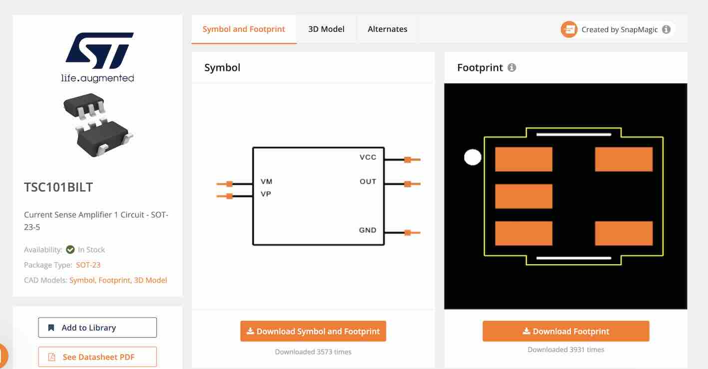
One of the best resources for finding ready-made KiCad libraries is SnapMagic (formerly SnapEDA).
The general workflow is:
- Search for the desired component.
- Download the schematic symbol.
- Download the PCB footprint.
- Import both into KiCad.
Useful resources:
-
SnapMagic Library: https://www.snapeda.com/home/
-
Import Guide: https://support.snapmagic.com/en/articles/5995733-how-to-import-into-kicad-v6-and-later
Option 2 — Create a Custom Component
If a component cannot be found online, a custom symbol and footprint can be created.
Helpful resources include:
-
SparkFun Tutorial: https://learn.sparkfun.com/tutorials/beginners-guide-to-kicad/creating-custom-kicad-schematic-components
-
Official KiCad Documentation: https://docs.kicad.org/9.0/en/getting_started_in_kicad/getting_started_in_kicad.html#tutorial_part_4_custom_symbols_and_footprints
Creating custom components requires additional work but provides complete flexibility when designing custom hardware.