Week 08 — Electronics production
Global Class
The global lecture focuses on fabricating and assembling a PCB, which becomes the foundation for all subsequent electronics work including input devices, output devices, and networking.
A key message is that future assignments depend on having a working board, not just a designed one.
PCB Fabrication Methods
Several fabrication approaches were presented:
- dead-bug wiring (manual wiring, not recommended)
- chemical etching (common but hazardous)
- CNC machining (Fab Lab standard workflow)
- laser-based methods
- vinyl cutting
Etching allows fine resolution but introduces environmental and safety concerns.
Machining is preferred in Fab Labs because it is:
- fast
- clean
- suitable for prototyping
The lecture highlighted that PCB production is a deterministic process:
- correct setup → consistent results
- errors → usually due to tool, material, or configuration
Assembly and Debugging
Soldering is not a secondary step but a core skill.
Important techniques:
- clean solder joints
- desoldering braid
- hot air rework
- fixing errors with jumper wires
Debugging is expected and part of the normal workflow.
Key Insight
PCB production can be summarized as:
design → fabrication → assembly → debugging → validation
A board is only complete when it runs code and behaves as intended.
Local Class
Remote Participation
Due to absence from the physical session, this week was documented through:
- review of classmates’ documentation
- observation of shared lab workflows
- comparison across Fab Academy repositories
Observed PCB Workflow
A consistent production process was identified:
- export design from KiCad
- generate toolpaths in Mods
- mill traces and outline
- clean, solder, and assemble
- test and debug
Key Observations
- correct milling depth is critical for trace isolation
- flat board setup strongly affects results
- soldering quality directly impacts functionality
- debugging is a normal and essential step
Common issues:
- broken or uncut traces
- solder bridges
- unstable programming connections
Key Insight
A PCB is only complete when it is:
- powered correctly
- programmable
- functionally verified
Weekly Assignment
Group Assignment
Here is the work we did for the group assignment:
Reflection and Learnings
- Understanding how stepper motors are controlled through multi-pin sequencing instead of simple STEP/DIR signals.
- Using a logic analyzer made it possible to visualize invisible signals and directly relate code → electrical signals → motion.
- Verified the importance of common ground and clean power for reliable measurements.
- LED feedback + signal capture is an effective layered debugging strategy.
- Reinforced the value of testing subsystems before integration
ASFALT relevance: This clarifies how to control actuators (future positioning, airflow, or mechanical movement) and how to debug signal behavior early before full system integration.
Personal Assignment — PCB Production Process
Goal
Produce a PCB using CNC milling by preparing files, generating toolpaths, and fabricating the board using a Roland SRM-20.
PCB Production Workflow
The workflow consists of:
- exporting traces and outline from KiCad
- generating toolpaths using Mods
- loading files to the Roland machine
- milling traces
- milling the board outline
- milling the holes
- cleaning and inspecting the PCB
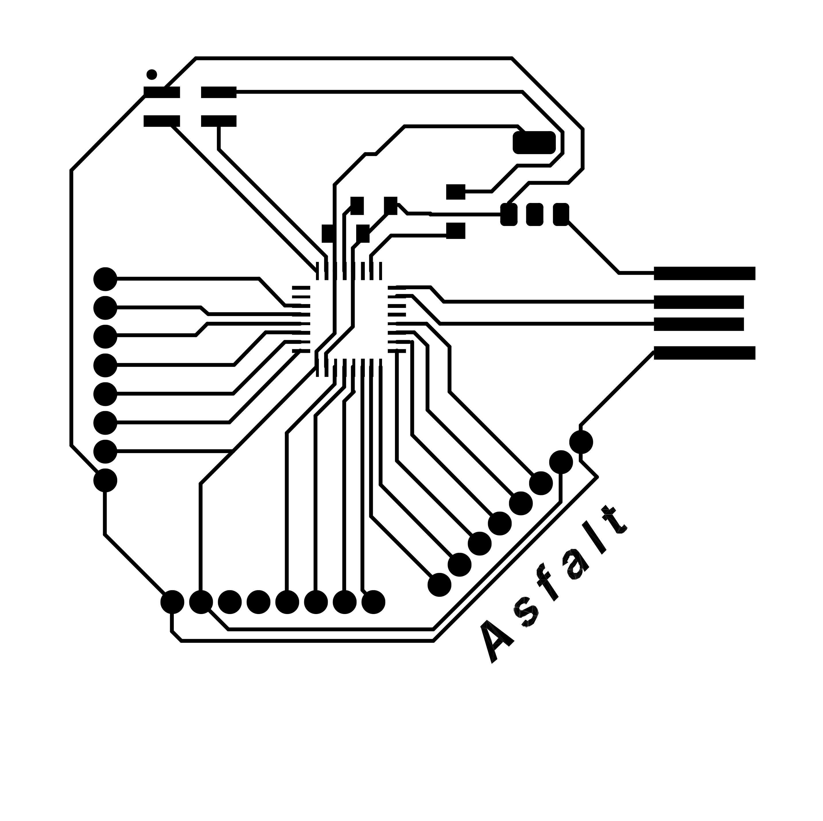
1. Exporting PCB from KiCad
The PCB design was exported from KiCad as vector graphics.
From this design, separate layers were prepared:
- traces
- holes
- outline
2. Preparing Files for Milling
2.1 Converting to Raster Format
The exported design was converted into PNG images to be processed in Mods.
I incorrectly saved the file as A4 and caused a lot of headaches because webpage kept crashing.
2.2 Inverting Colors
For proper toolpath generation:
- white = copper to keep
- black = material to remove
Traces

Holes

Outline

3. Generating Toolpaths in Mods
The prepared PNG files were imported into Mods.
Key Settings
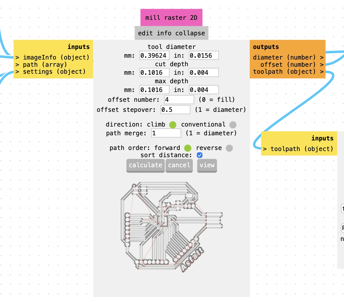
- tool diameter: 0.396 mm
- cut depth: 0.1016 mm
- max depth: 0.1016 mm
- offset number: 4
- offset stepover: 0.5
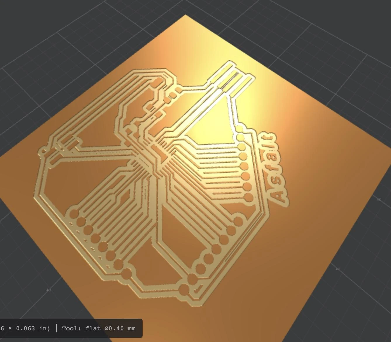
Toolpath Preview
Before milling, the toolpath was simulated:
4. Machine Setup (Roland SRM-20)
5. Milling Process
5.1 Bed Preparation
The sacrificial layer was cleaned to ensure a flat surface.
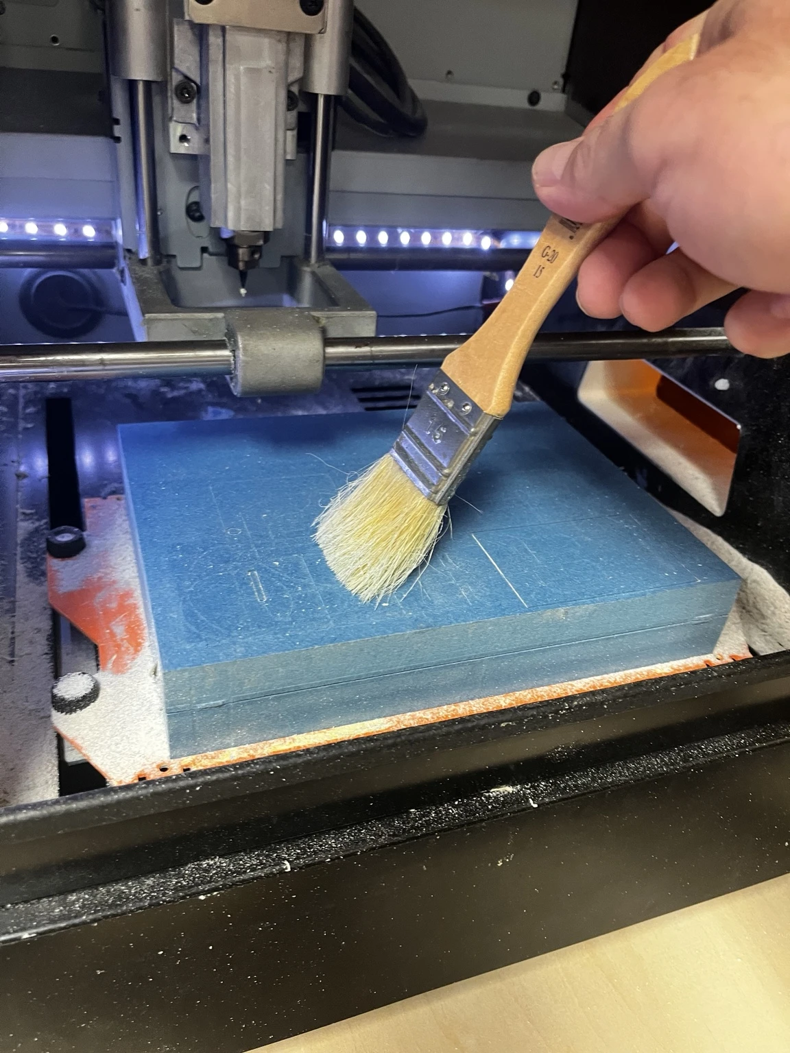
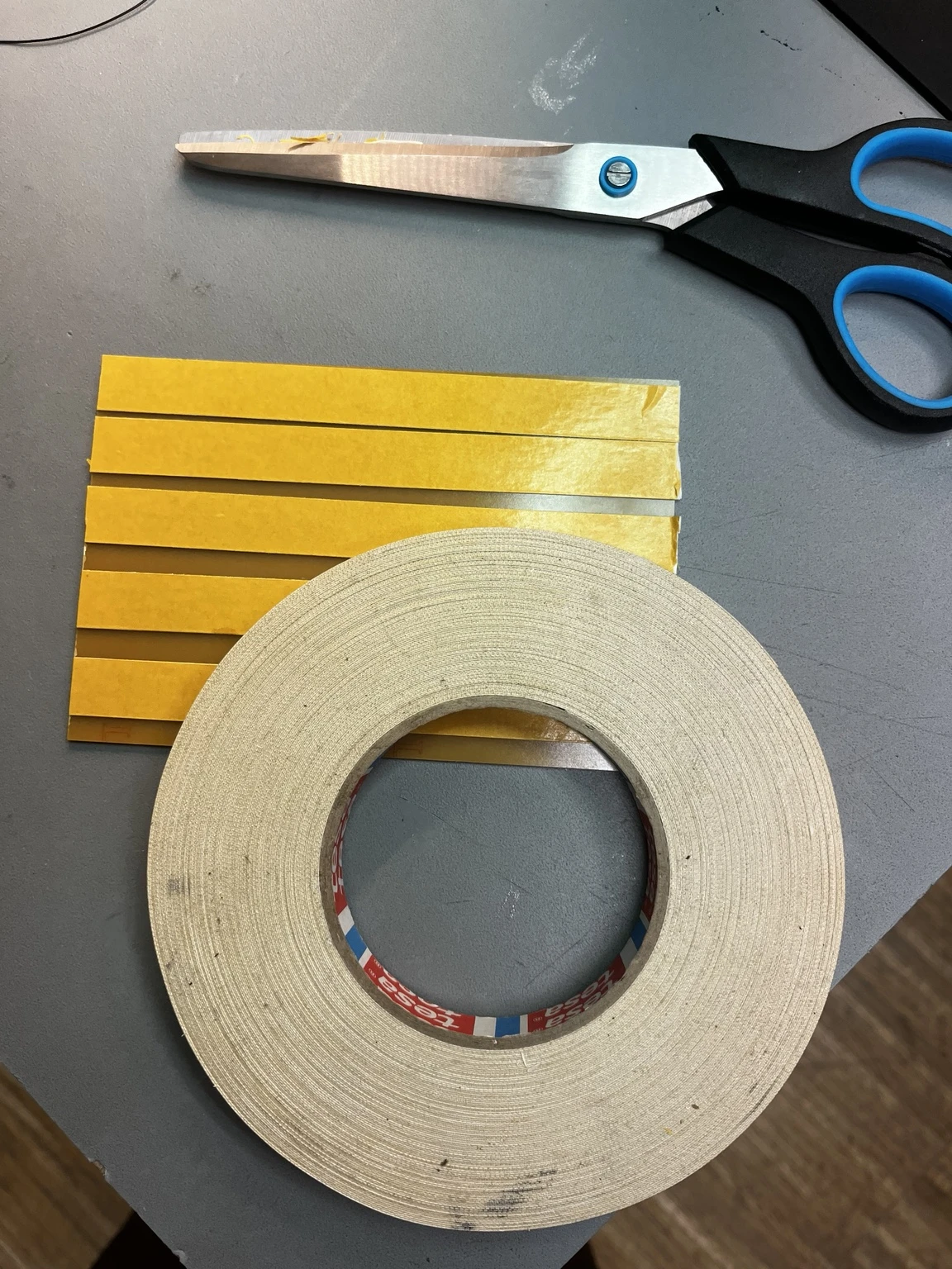
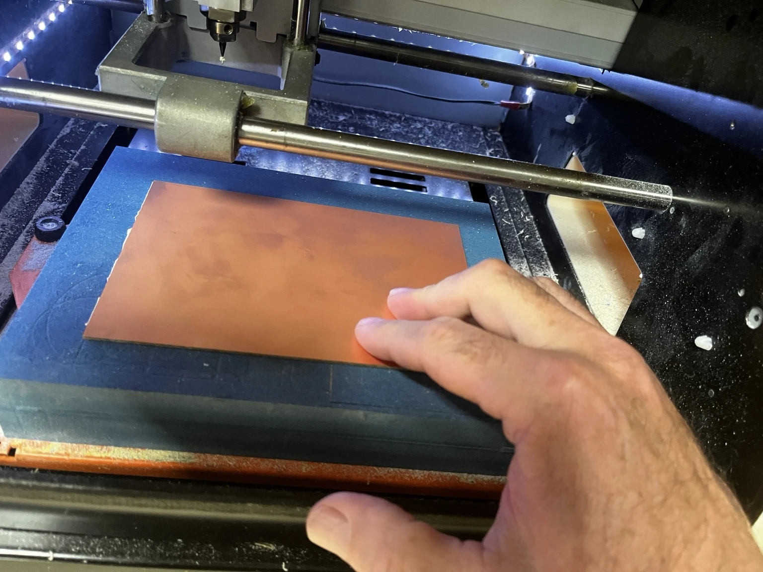
5.2 Fixing the PCB Material
The FR1 board was fixed using double-sided tape.
The generated toolpaths were loaded into the Roland machine using VPanel.
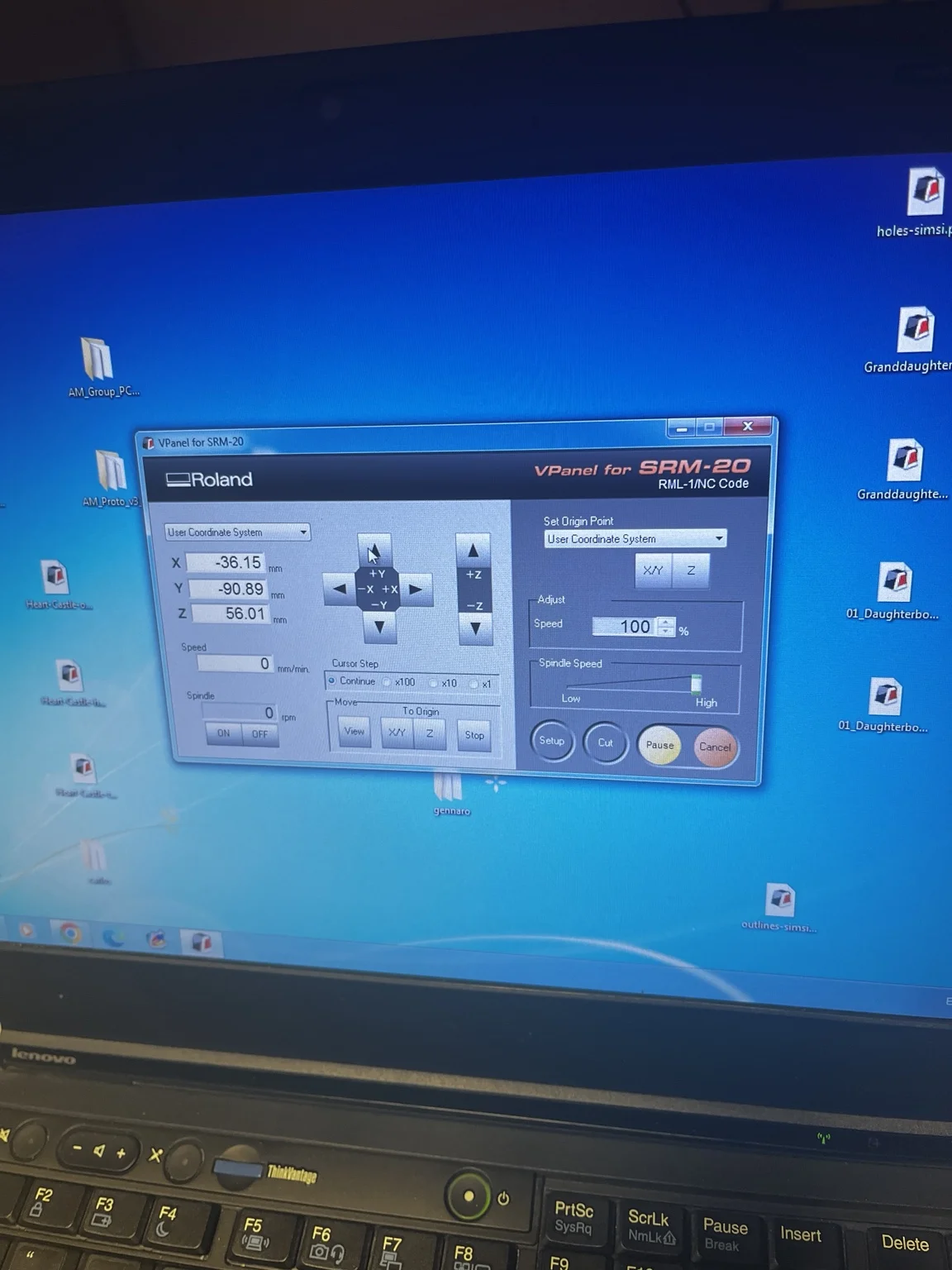
Steps:
- set XY origin
- manually lower tool to surface for Z origin
- verify spindle speed and movement
- load milling file
5.3 Z-Probing
The tool was carefully lowered to define the Z zero reference.
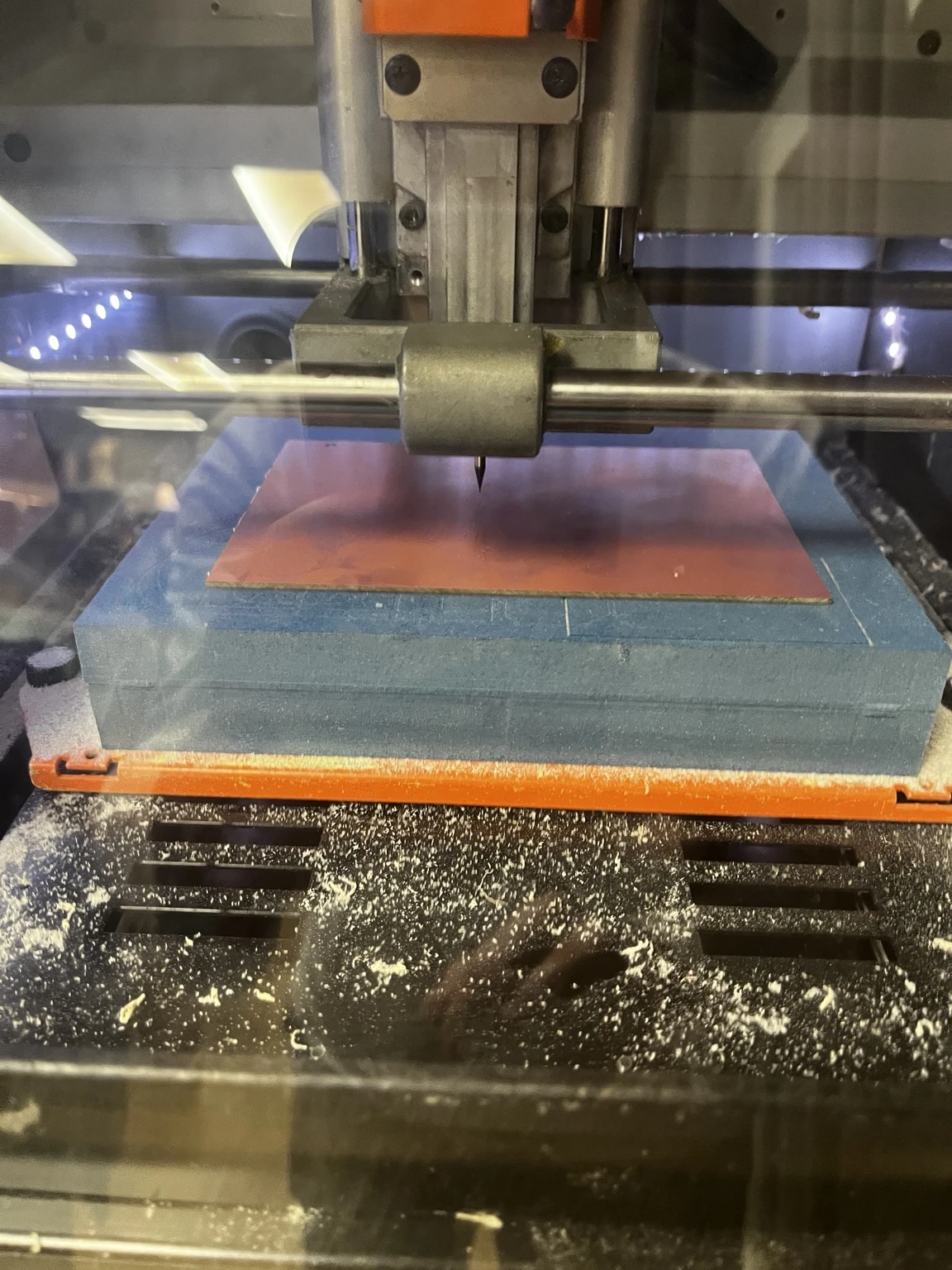
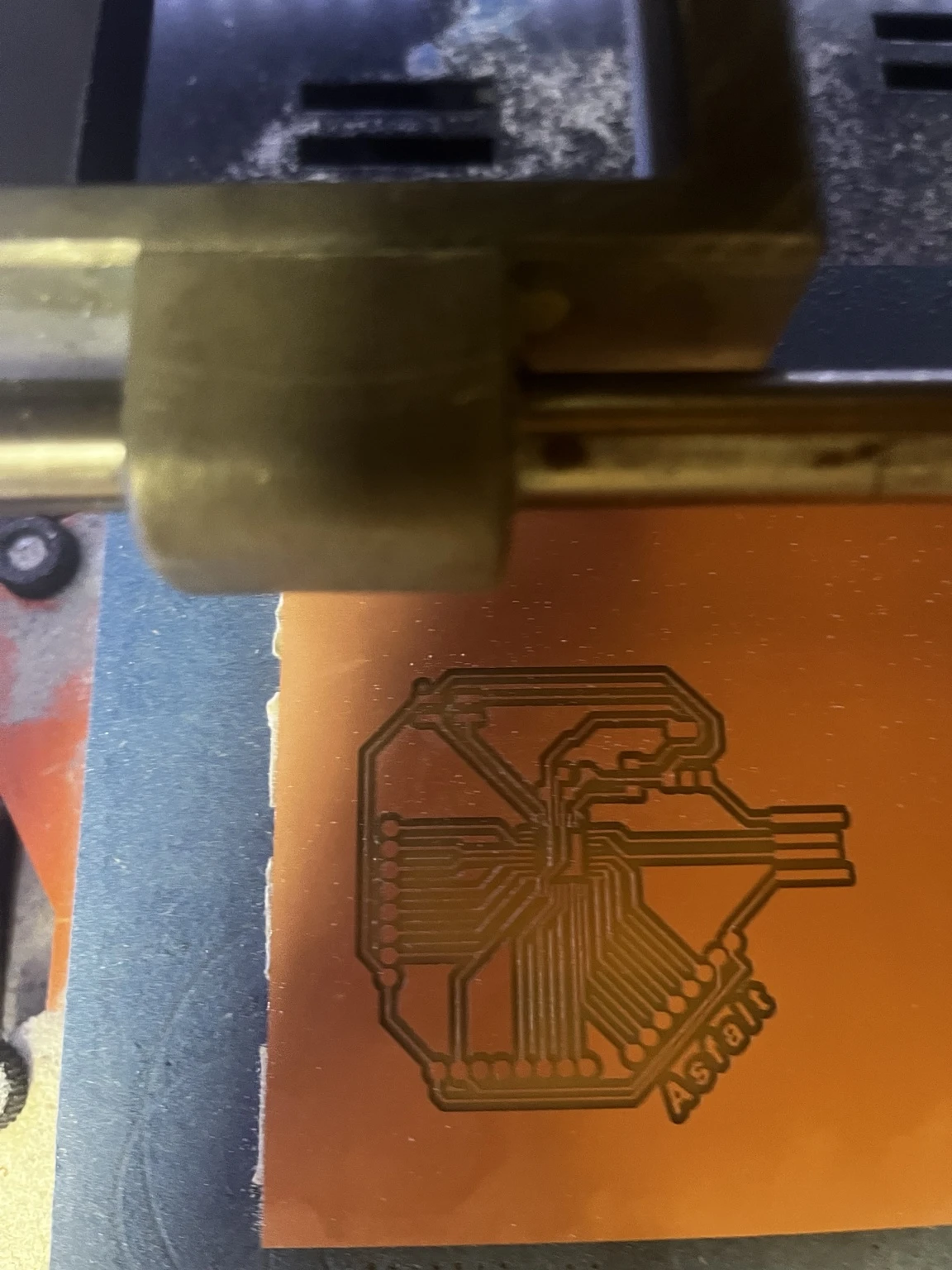
5.4 Milling Traces
The traces were milled using a 1/64” tool.
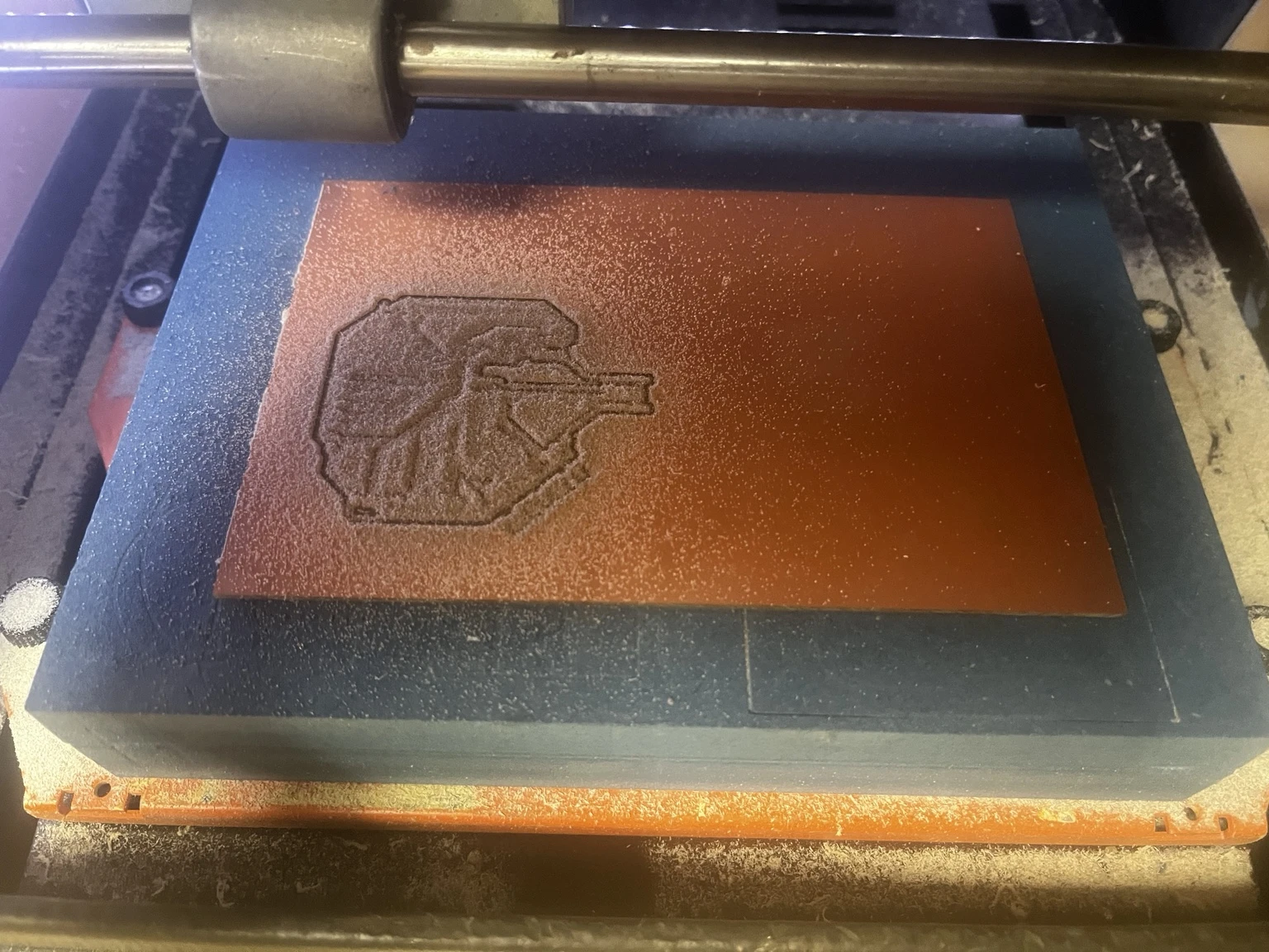
Everything was looking fine so far:
5.6 Cutting the Outline and milling holes
The board outline was milled using a larger tool.
Suddenly noticed that the outline and holes were not my design!
Apparently, the person who used the mill before me paused their work and didn’t cancel it. Even though I deleted previous files from queu, this little detail caused the machine to mill the pending file.
Anyways, had to start over with this in mind…
5.5 Re-milling
Now updloaded files for holes and outlines and came out correctl:
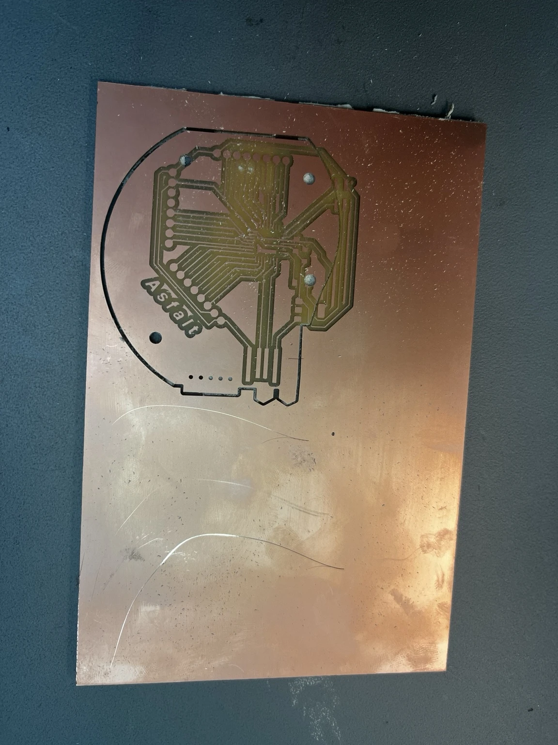
6. Cleaning and Inspection
After milling, the board was cleaned and inspected.
Looking good (according to me…)
7. Detail Inspection
Close inspection of traces revealed issues in fine-pitch areas. Reviewing with Dani and Adai, for no apparent reason, the machine didn’t mill the pins properly.
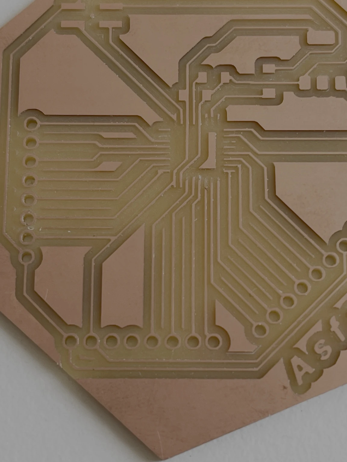
I have to go back and figure out what went wrong and redo the milling to get clean traces.
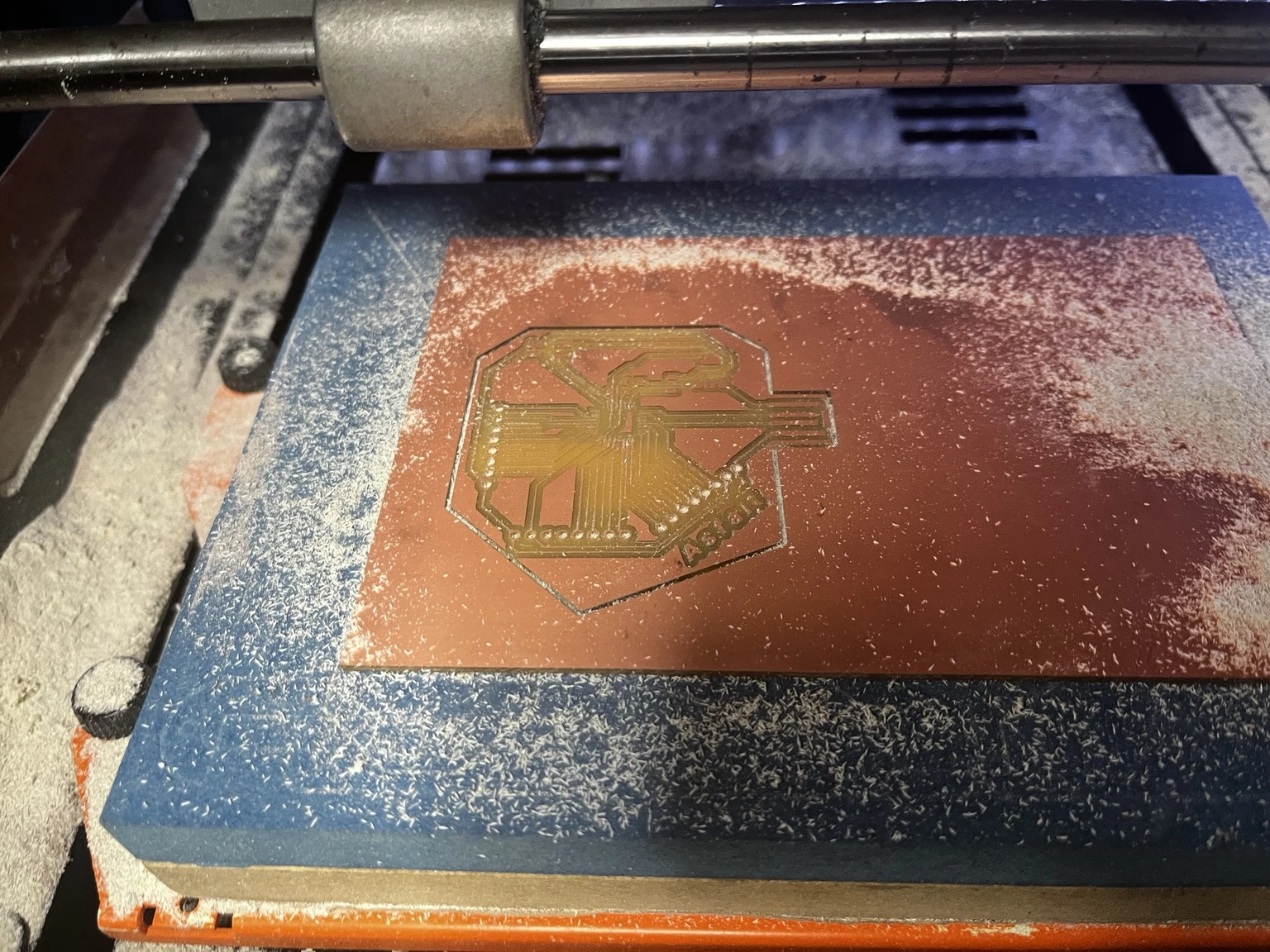
8. Re-Milling Attempts
After identifying issues in the first milled board (particularly in fine-pitch areas), I attempted to mill the PCB again to verify whether the problem was related to setup, toolpath, or machine conditions.
A new board was prepared and the same workflow was repeated:
- same PNG inputs
- same Mods settings
- same tool (1/64”)
- same machine (Roland SRM-20)
The result is shown below:
Observations
- Milling depth is uneven
- Pins still show poor definition
- Some traces appear merged together
- Trace edges indicate tool wear
Preliminary Diagnosis
After showing the board to Dani, we concluded that wrong end mill, tool wear or tip condition may be the causes of the failed attempted.
Agreed to re-mill useing V-bits instead as they were a prefereed tool in Fablab anyways. So back to mods.
Milling Failures and Iterations
After initial milling attempts, multiple issues were identified during the fabrication process. Two additional milling trials were carried out to diagnose and correct errors.
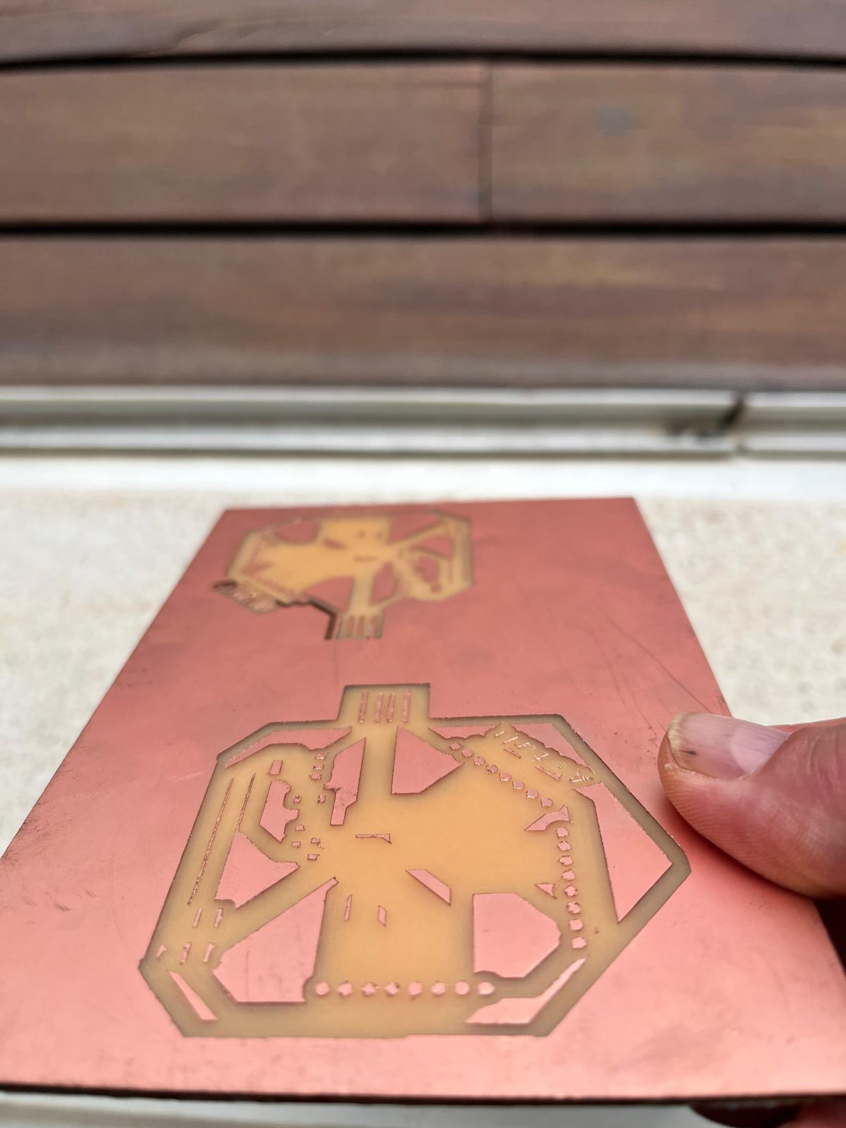
1. Incorrect Hole Placement (File Error)
In this attempt, the holes were milled in incorrect positions. This was traced back to an error in the exported file used for toolpath generation.
- Hole positions did not align with pads
- Likely mismatch between trace and hole files (offset or wrong layer export)
- Resulting board is unusable for component placement
2. V-bit Milling Issues (30° Tool Too Aggressive)
A second attempt was made using a 30° V-bit to improve trace resolution. However, the results showed over-milling and loss of detail.
- Traces became too thick and merged in fine-pitch areas
- Tool removed excessive copper due to incorrect depth/angle combination
- Fine features around the MCU pins were not preserved
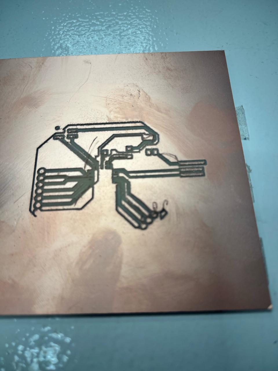
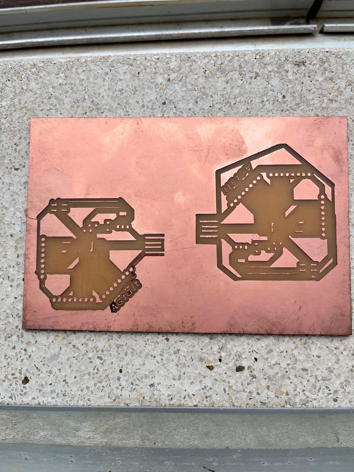
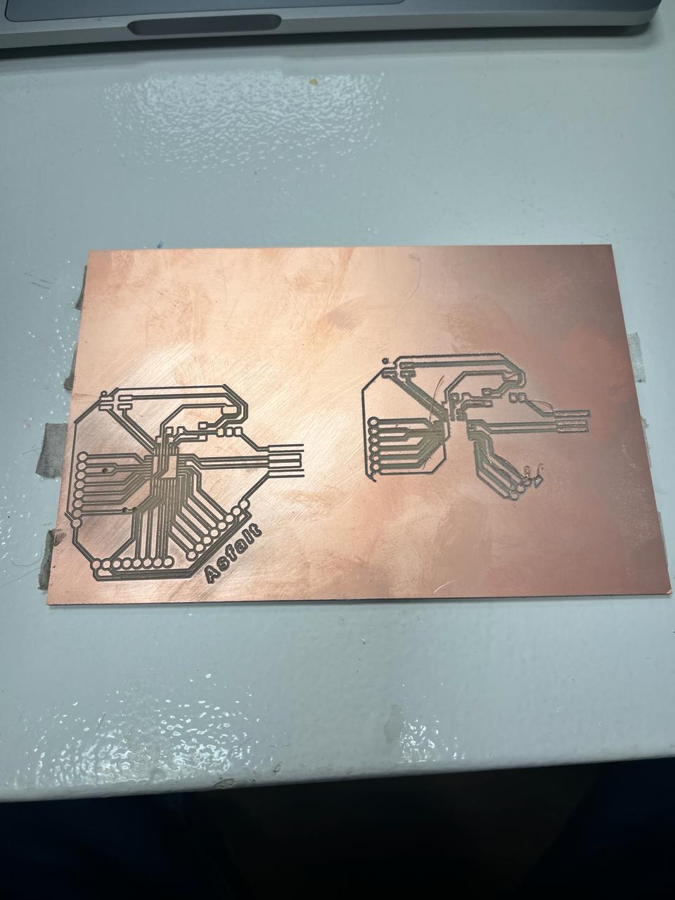
3. Overview of Failed Iterations
This image shows both failed attempts on a single copper board.
- file preparation (alignment and export)
- tool selection (flat end mill vs V-bit)
- milling parameters (depth, offsets)
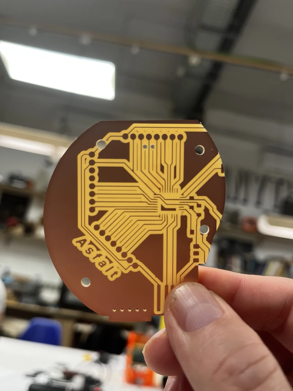
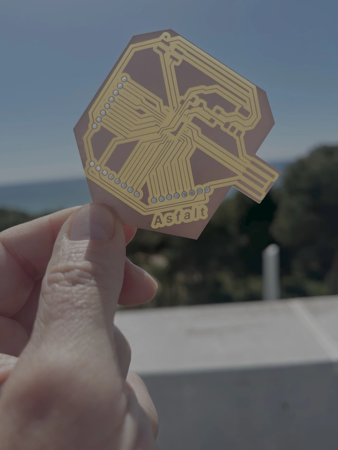
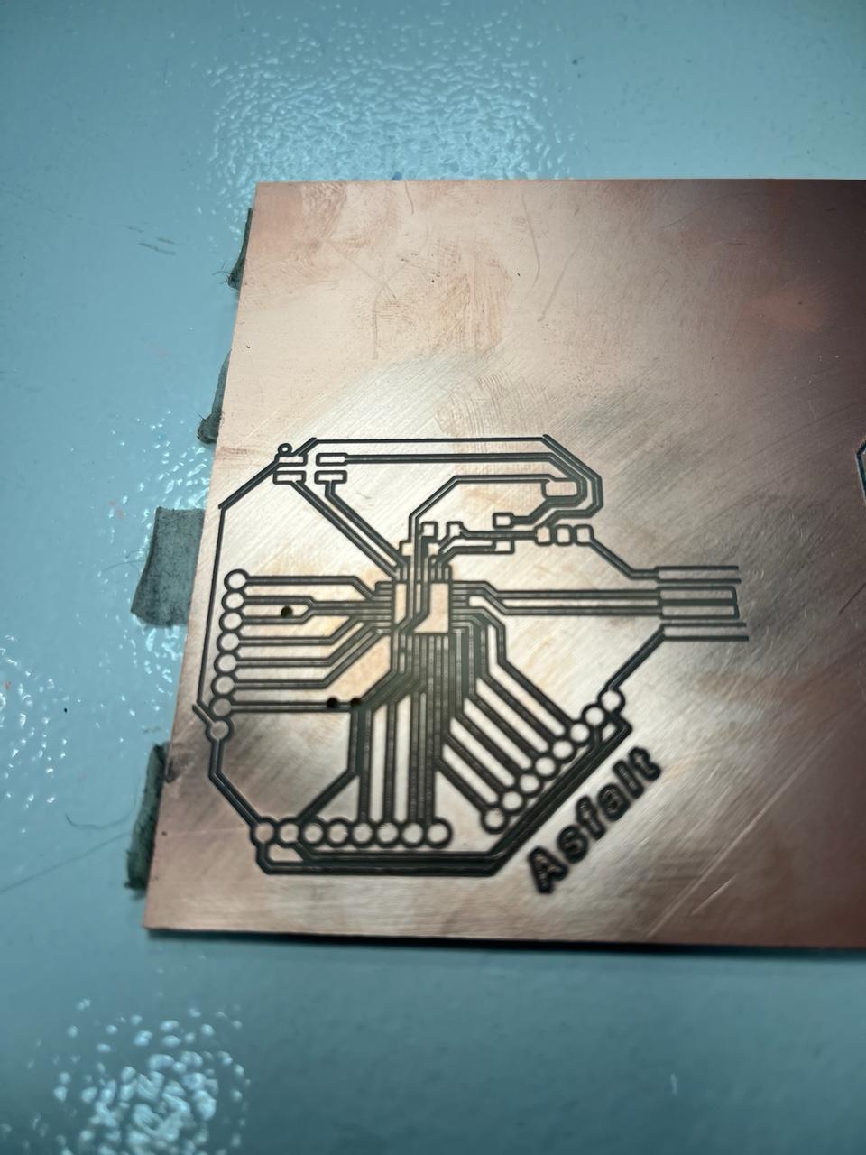
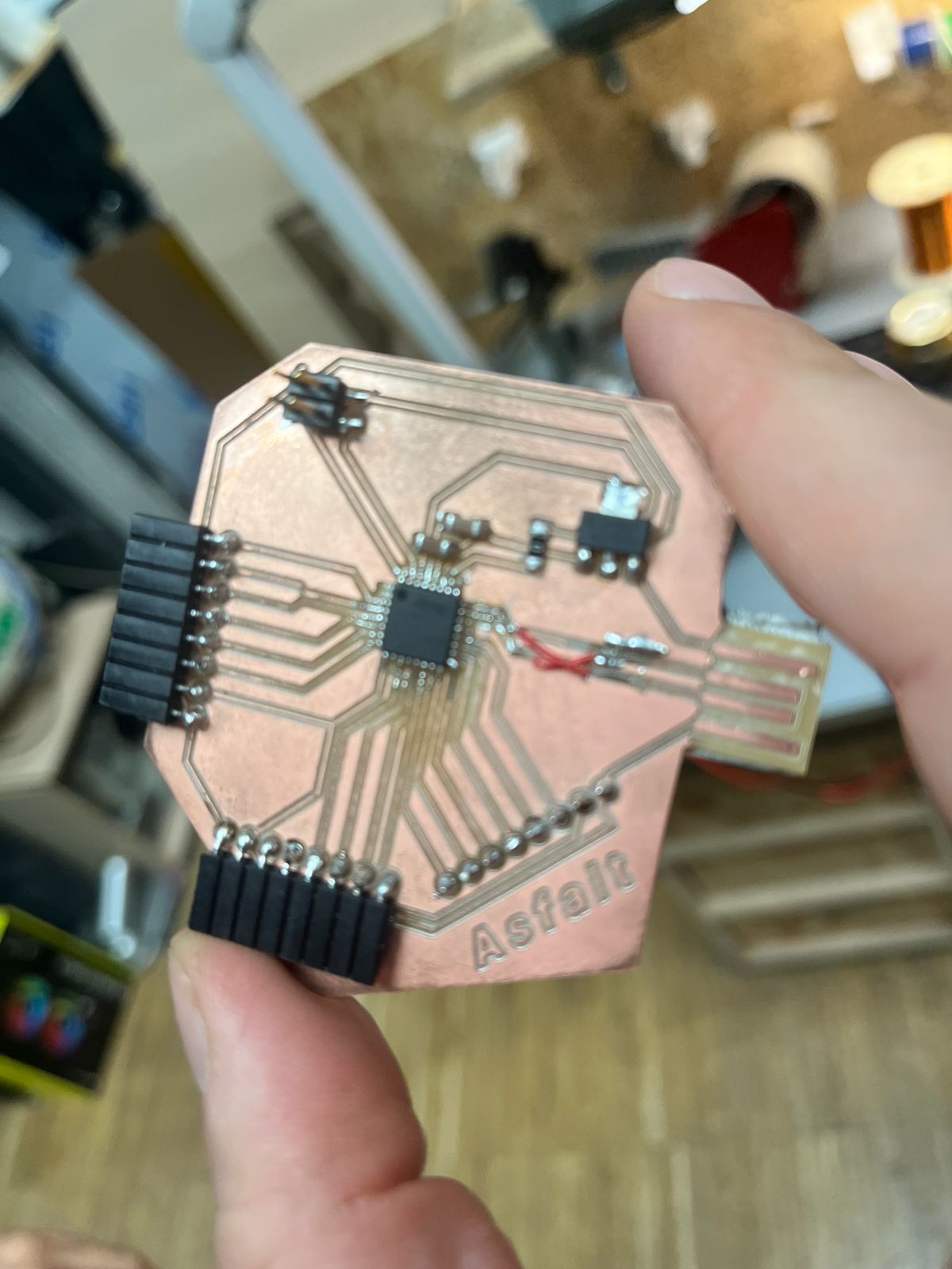
Final PCB – Successful Milling
After several failed attempts, a final milling pass produced a clean and usable PCB.
Finally!!!
- Traces are clearly defined with consistent width and proper isolation
- Fine-pitch areas around the SAMD21 footprint are preserved and separations are visible
- Holes are correctly aligned with pads, confirming proper file preparation and alignment
- No trace merging or excessive copper removal
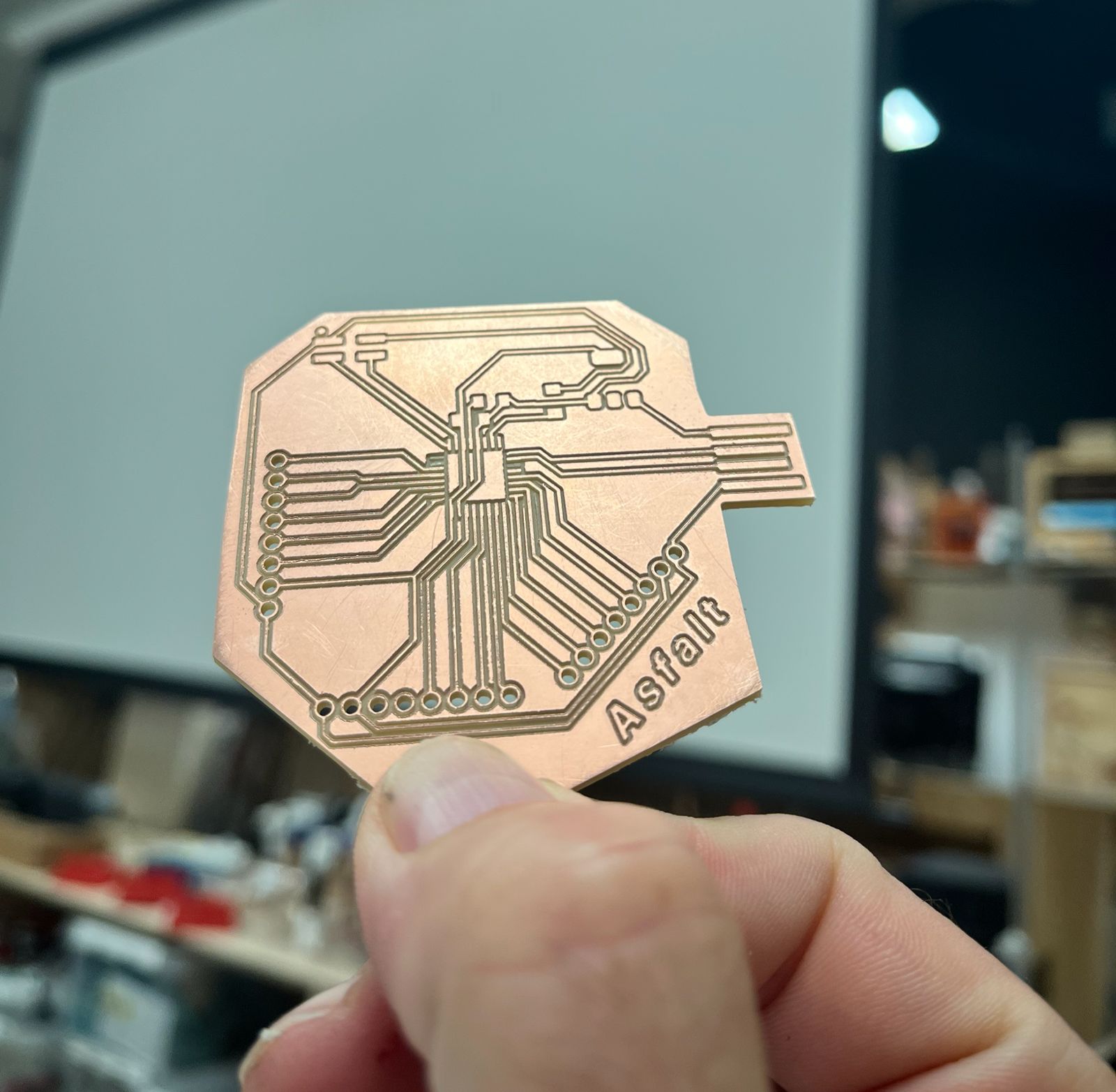
This result was achieved by correcting:
- file preparation workflow (traces, holes, offsets, background colors, inverted image, etc.)
- tool selection and calibration (appropriate bit and depth)
- milling parameters (cut depth and offsets tuned)
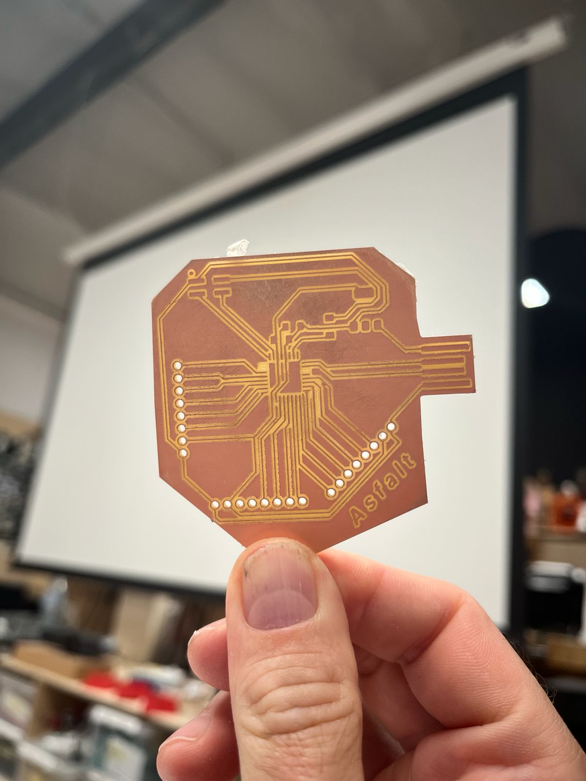
The board is now suitable for component soldering and further testing.
Board Validation and Programming Preparation
After soldering the components onto the final PCB, I started validating the board before attempting to program the SAMD21 microcontroller. Dani helped me troubleshoot and verify the next steps of the process.
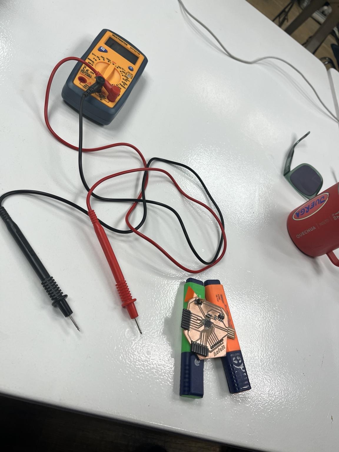
Electrical Continuity Testing
The first step was checking that the PCB connections were electrically correct using a multimeter in continuity mode.
Each header pin was tested individually:
- touching one probe to the pin
- touching the second probe to the corresponding trace or microcontroller connection
The multimeter beep confirmed that the electrical path existed correctly. I also tested adjacent pins to ensure they were NOT shorted together. This helped verify:
- traces were connected properly
- no accidental solder bridges existed
- pins remained electrically isolated where required
The board passed the continuity checks successfully.
Preparing the SAMD21 for Programming
With the board electrically validated, I proceeded to set up the software environment for programming the SAMD21 microcontroller.
This required:
- opening Arduino IDE
- installing the SAMD board definitions
- configuring the programming environment
- preparing the bootloader upload process
The goal was to upload a basic test program such as a blink example to verify that:
- the microcontroller was powered correctly
- USB communication worked
- the programming interface was functional
Discovering a Power Regulation Issue
During the blink test, the board was not responding correctly. After checking software settings and connections, I returned to electrical debugging.
A second voltage inspection, Dani disconvered that the wrong voltage regulator had been soldered onto the PCB.
Instead of:
- AMS1117-3.3V
I had accidentally soldered:
- AMS1117-5V
This explained why the SAMD21 was not behaving correctly, since the microcontroller is designed to operate at 3.3V.
Although I could not determine exactly how the wrong part was selected during assembly, identifying the mistake was an important debugging step.
Reworking the PCB
To fix the issue:
- the incorrect regulator was desoldered using hot air
- the pads were cleaned
- the correct AMS1117-3.3 regulator was soldered back onto the board
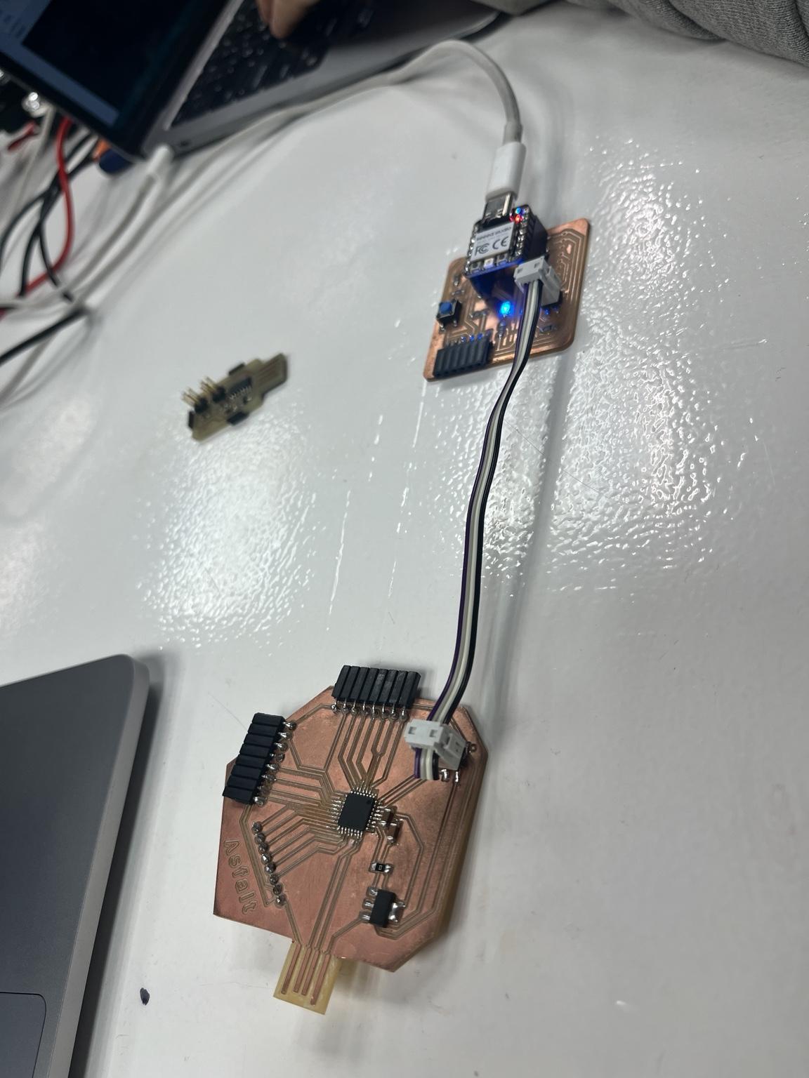
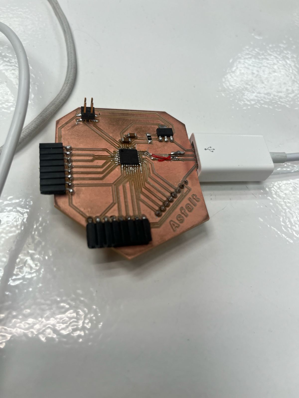
Programming and Final Board Test
After the board was soldered and electrically checked, the next step was to program the PCB and confirm that it could run a basic test.
The plan was to upload a simple blink test using the Arduino IDE. However, the board was not recognized through USB.
At this point, the board had already passed basic continuity checks, so the issue seemed related to the USB connection rather than the general soldering.
USB Trace Debugging
Dani helped inspect the PCB layout and noticed that the USB data traces appeared to be inverted.
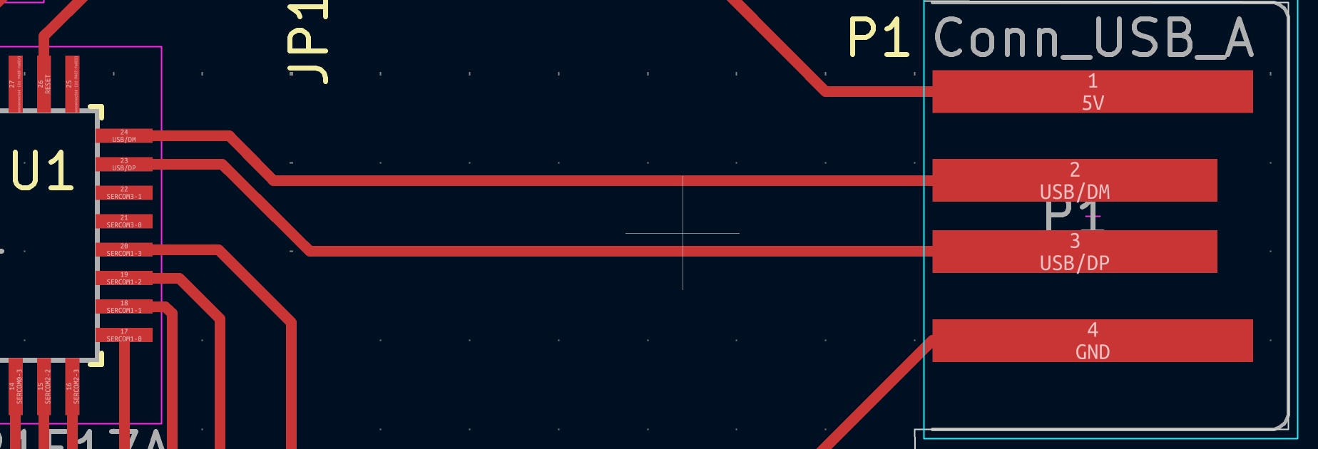
The USB connector lines did not match the expected USB D+ and D- routing. This meant the computer could not correctly detect the board.
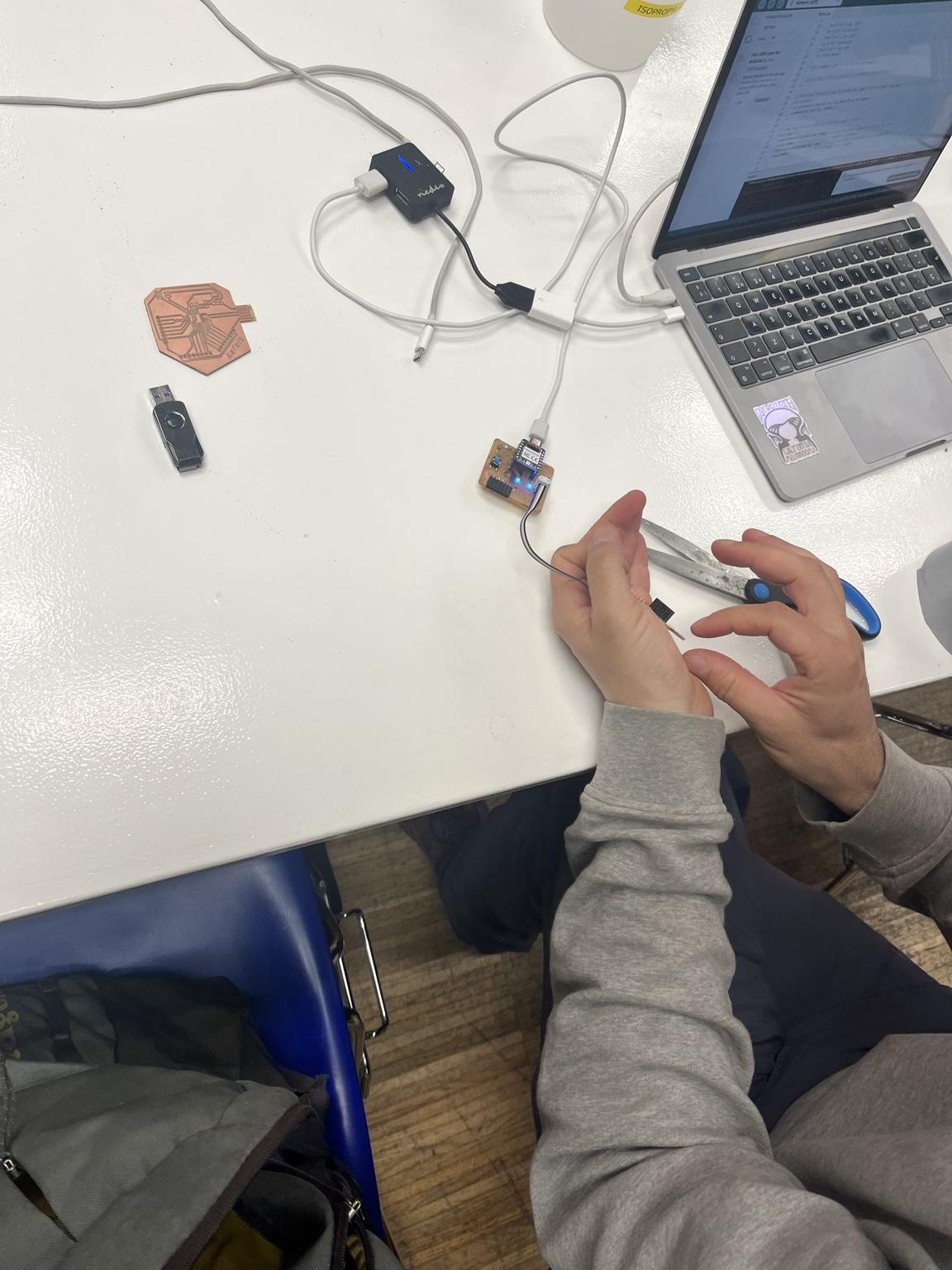
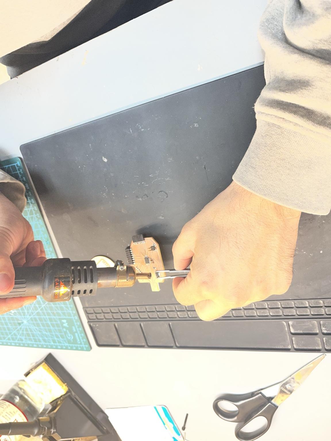
PCB Rework
After debugging the board, Dani identified that the USB data traces were inverted on the PCB layout. This prevented the computer from correctly recognizing the SAMD21 board through USB.
To temporarily solve the issue, we decided to bypass the incorrect traces manually using small jumper wires.
First, very small wires were prepared by stripping thin cable ends that could later be soldered directly onto the PCB traces.
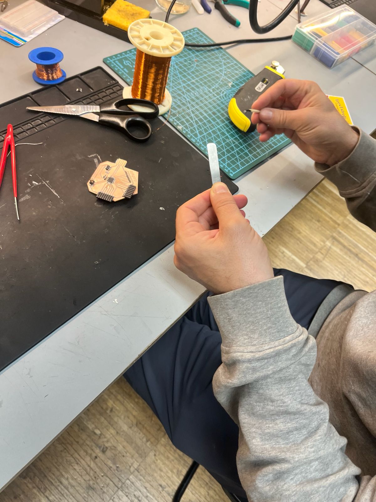
After preparing the wires, continuity and signal paths were checked again with the multimeter to understand exactly where the incorrect USB routing was located.
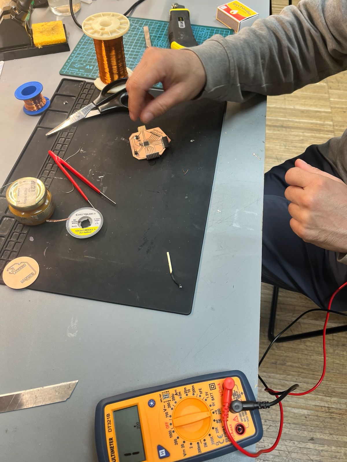
Once the correct USB data paths were identified, the jumper wires were soldered directly across the PCB to bypass the incorrect traces.
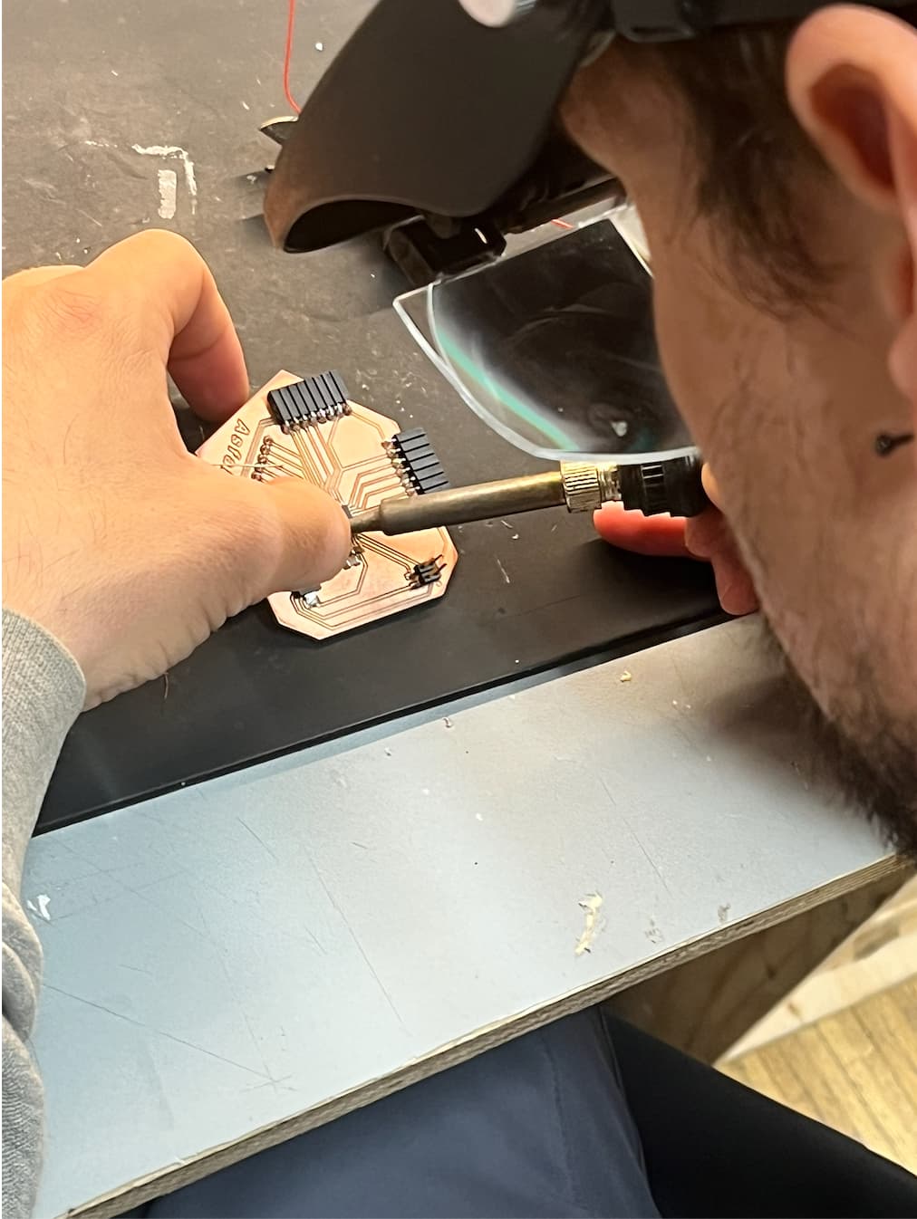
The final rewired PCB connected the USB lines correctly and allowed communication with the computer.
After reconnecting the board, the PCB was finally recognized correctly by Arduino IDE and the programming test could continue.
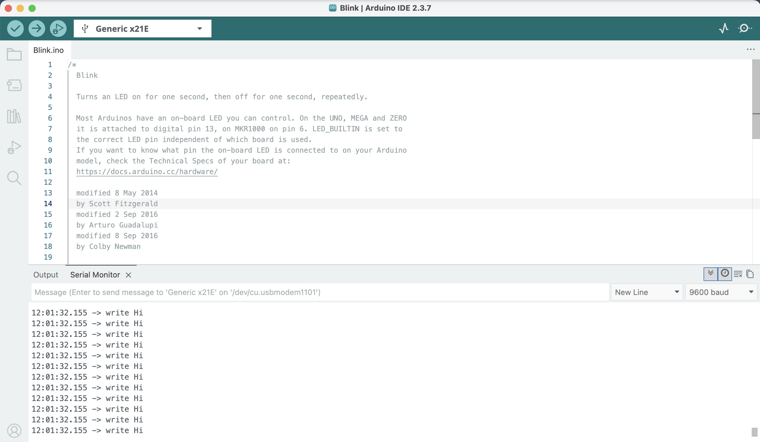
Blink Test
Once the board was recognized, I uploaded a simple blink-style test. Instead of using only one LED pin, the code looped through multiple pins and switched them HIGH and LOW while printing messages to the Serial Monitor.
void setup() {
  Serial.begin(115200);

  for (int i = 0; i < 12; i++) {
    pinMode(i, OUTPUT);
  }
}

void loop() {

  for (int i = 0; i < 12; i++) {
    Serial.println("write Hi");
    digitalWrite(i, HIGH);
  }

  delay(1000);

  for (int i = 0; i < 12; i++) {
    Serial.println("write Low");
    digitalWrite(i, LOW);
  }

  delay(1000);
}
The serial output confirmed that the program was running correctly on the SAMD21 board.
Learnings
With Dani’s help, the board was successfully debugged, recognized through USB, programmed through Arduino IDE, and tested with a basic output program.
The assignment objective was completed: the PCB was designed, fabricated, soldered, electrically tested, programmed, and verified.
However, this board should not be reused directly for the final ASFALT hardware. The USB trace issue and the amount of manual rework show that the PCB needs to be redesigned before becoming part of a more reliable project system.
Reading back on the notes from GLobal Class, the lecture highlighted that PCB production is a deterministic process:
- correct setup → consistent results
- errors → usually due to tool, material, or configuration
This was definetly the case.
References and AI Use
- Mods Project (MIT Center for Bits and Atoms) https://modsproject.org
- Roland SRM-20 documentation from Fablab Barcelona
- Custom GPT used for structuring workflow and documentation formatting
Prompts
-
“Explore different paths to write code to program ASFALT hardware.”
-
“Make a plan to execute on the electronic part of ASFALT project.”
-
“Evaluate if the drawing and tracing could’ve caused the milling failure.”
-
“Look for open source designs relevant to thermal control systems like reflow ovens or sous-vide controllers.”
-
“Check schematics to identify power, communication, inputs, outputs, and programming sections.”