Project Fabrication
Project Overview
My final project is an electric saxophone. The minimum viable product that fulfills the requirements consists of a 3D printed PLA housing with the dimensions of an alto saxophone, where the user breathes into a piezoresistive gauge pressure sensor through a regular mouthpiece and pushes switch buttons. The buttons are all connected to a daughterboard with multiple microcontrollers that communicate via I2C with the motherboard, where the pressure sensor is connected, and through which the inputs get transformed into I2S signals which get sent to a speaker through an amplifier.
After being able to integrate all this for the presentation, the plan is to try and spiral the project in the following ways:
- Not only measuring the breath pressure, but also the breath flow, so that the oscillation of both values changes the frequency and pitch of the sound. (In my research, I saw somebody else that was building an electronic saxophone who tried to produce the same effect by putting a force-sensitive resistor sensor between his mouthpiece and reed, where the resistor was half of a voltage divider, so that the voltage in the middle varied with the force on the reed and in turn varied the sound being output. However, I want to be able to use regular mouthpieces in mine so I will go this different way)
- Making the buttons as similar as possible to the keys of a regular saxophone in both shape and feeling. I had already managed to acomplish a realistic emulation of actual saxophone keys, but they were not structurally resilient enough. So there is work to do in strengthening them repetitive use. Feeling wise, I can play with the springs on the keys and how they interact with the PCB. Thisspiral would require to move away from switch buttons and back to hall effect analog sensors, meaning the current microcontrollers are still ideal.
- Keeping the switch buttons on the keys and replacing the current microcontrollers for the ESP32S3 modules, due to my familiarity with them and with the communication being easier between them and the RP2040.
- Making it so that the Neopixel ring on the mouth of the bell interacts with the noise bein produced.
- Adding small neopixel rings and LCD screens to the screw-on modules along the bow and bell of the saxophone, where the neopixels either interact with each other, or reflect the battery life of the instrument, and where the LCD screens either show what note is being played or show the battery life of the instrument.
Timeline
| Task | Timeframe |
|---|---|
| Overall electronic system design. | 2 weeks |
| Electronics PCB design. | 2 weeks |
| Electronics PCB milling and soldering. | 1 week |
| Mechanical parts design. | 1 month |
| Mechanical parts printing. | 2 weeks |
| Electronics programming and troubleshooting. | 3 weeks |
| Mechanical parts assembling. | 2 weeks |
| Presentation (slide and video) preparation. | 1 day |
Index of Processes Used
2D Design
Electronic systems schematic design in Kicad
- General electrical circuit design
- Programmer circuit design
- Motherboard circuit design
- Daughterboard circuit design
- Granddaughterboard circuit design
PCB design in Kicad
- Programmer PCB design
- Motherboard PCB design
- Daughterboard PCB design
- Keys granddaughterboard PCBs design
- Pressure sensor granddaughterboard PCB design
3D Design
Mechanical parts design in Fusion
- Neck
- Body
- Keys
- Bow
- Bell
Additive Fabrication
Fillament extrusion 3D printing
- Reed
- Neck
- Body
- Keys
- Bow
- Bell
Subtractive Fabrication
Acrylic laser cutting
PCB CNC milling
- Programmer PCB milling
- Motherboard PCB milling
- Daughterboard PCB milling
- Keys granddaughterboard PCBs milling
- Pressure sensor granddaughterboard PCB milling
Embedded Microcontroller PCB
Programming
- Programmer programming
- Motherboard programming
- Daughterboard programming
Interfacing
System Integration: Techniques and Applications
PCB and electrical components mounting
- Programmer PCB mounting
- Motherboard PCB mounting
- Daughterboard PCB mounting
- Keys granddaughterboard PCBs mounting
- Pressure sensor granddaughterboard PCB mounting
- Speaker mounting
Mechanical parts alignment
Wire harnesses guiding
Surface finishing
- Neck
- Body
- Keys
- Bow
- Bell
Bill of Materials
| BoM Level | Part Name | Description | Manufacturer | Distributor | Unit Price | Qty | Total Price | |
|---|---|---|---|---|---|---|---|---|
| 1 | Electronics | Xiao RP2040 | Microcontroller | Seeed Studio | 2 | |||
| 2 | Electronics | AVR128DB32-I/PT | Microcontroller | Microchip Technology | Mouser.com | 1.86€ | 2 | 3.72€ |
| 3 | Electronics | MAX98357 | I2S Class-D Mono Amplifier | Adafruit | Mouser.com | 5.65€ | 1 | 5.65€ |
| 4 | Electronics | MPXM2010GS | Air Pressure Sensor | NXP USA | Digikey.com | 9.74€ | 1 | 9.74€ |
| 5 | Electronics | 8 ohm Speaker | Speaker | 1 | ||||
| 6 | Electronics | SMD LED | LED | 5 | ||||
| 7 | Electronics | 10K OHM 5% 1/16W 0402 | Resistors | Yageo | Digikey.com | 0.09€ | 22 | 1.98€ |
| 8 | Electronics | 1K OHM 1% 1/4W 1206 | Resistors | Yageo | Digikey.com | 0.09€ | 5 | 0.45€ |
| 9 | Electronics | 499 OHM 1% 1/4W 1206 | Resistors | Yageo | Digikey.com | 0.09€ | 1 | 0.09€ |
| 10 | Electronics | 1uf | Capacitors | 6 | ||||
| 11 | Electronics | 100nf | Capacitors | 4 | ||||
| 12 | Electronics | Push Buttons | Switches | Samesky | 22 | |||
| 13 | Mechanical | Black Matte PLA | Filament | Bambulab | Bambulab.com | 25.99€ | 2 | 51.98€ |
Documentation
Electronics
General Electrical Circuit
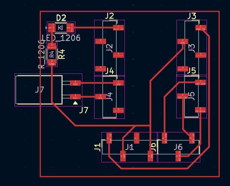
Initially, I thought about using the AVR128DB64 microcontroller on a motherboard and having all the inputs go directly into it, like you can see below:
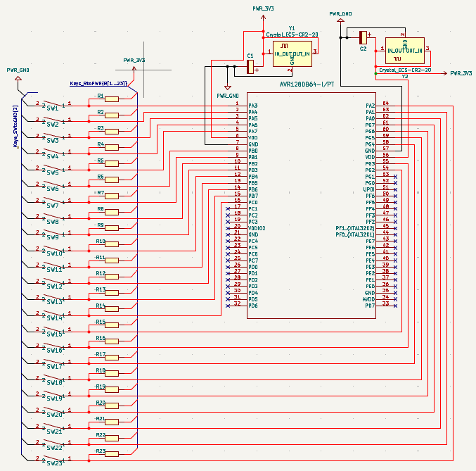
After speaking with Dani, we discussed that a better approach might be to have daughterboard going into the main motherboard so as to simplify things. So instead of a single pcb with a ridiculous amount of inputs, I decided to have the left hand keys go into one board, the right hand keys go into another board, the breath chamber sensors go into another board, and have all 3 of these boards go into the main motherboard. So instead of using the AVR128DB64 microcontroller, I decided to use the AVR128DB32 microcontroller for all 4 boards. Based on this approach, I began by developing the daughterboard for the left hand keys and the granddaughterboard(s) for the input devices going into it.
The overall electronic schematic can be found here.
Programmer
In order to program the AVR128DB32 microcontrollers on all of my daughterboards and the motherboard, I designed a UPDI programmer based off the Quentorres. I removed the original Quentorres' SWD components and turned the UART connector into a UPDI connector, putting the resistors between the TX and RX lines on the board itself. So the design looked like this:
But since I didn't want to solder the Xiao RP2040 directly into the board, I put vertical pin sockets so that I could remove it if needed. So the PCB design ended up lookig like this:
After following the workflow for our in-house production, I got to milling (where I forgot to take a picture), and then soldering the components in, so my programmer looked like this:
I followed the instructions on the Quentorres Documentation page to set the programmer up.
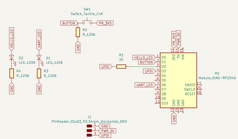
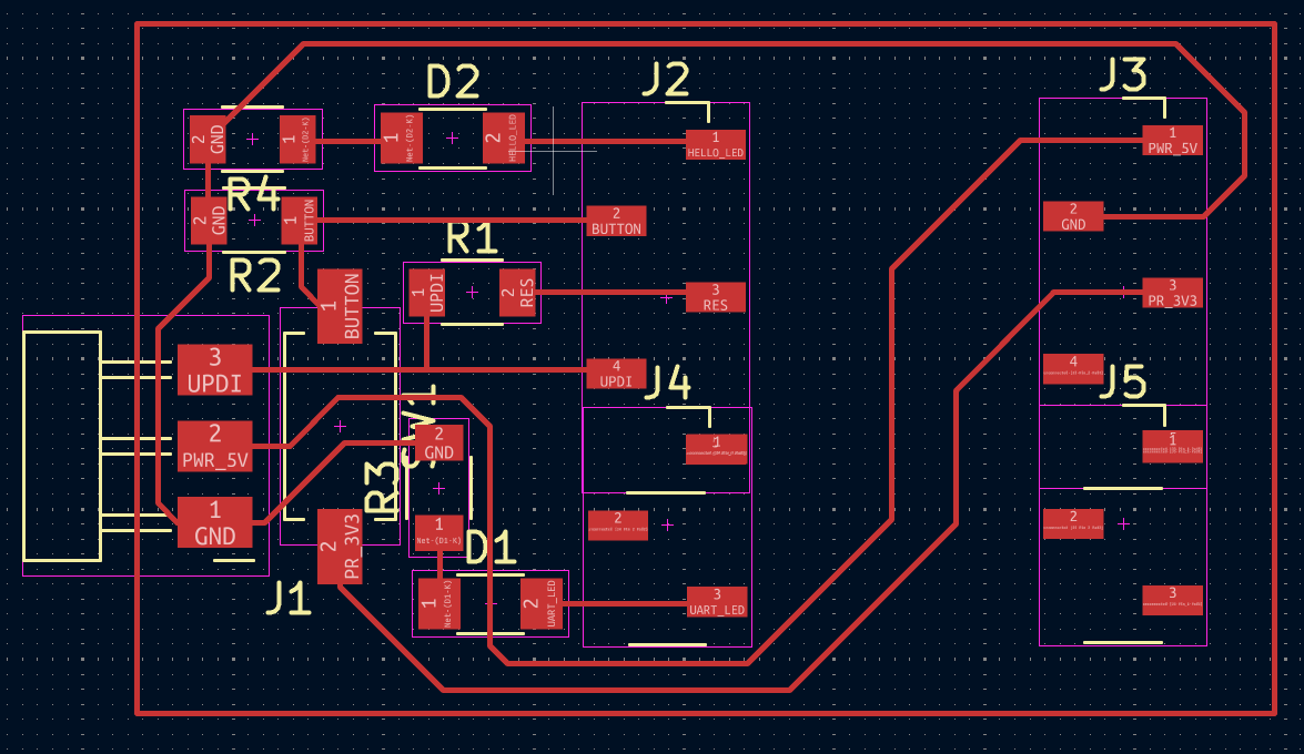
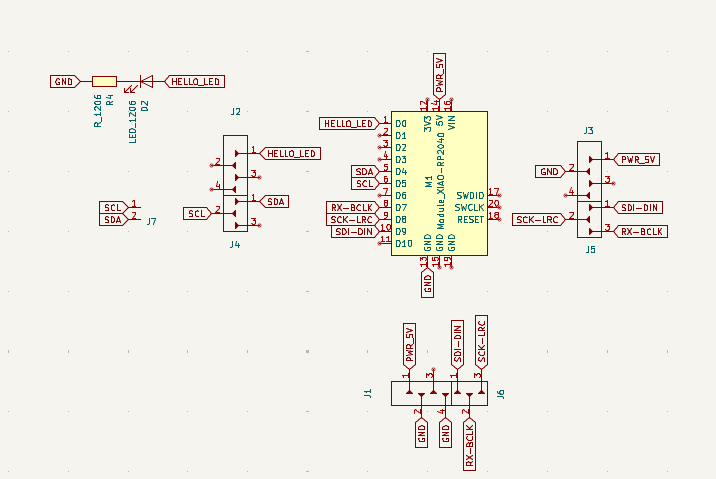
Motherboard
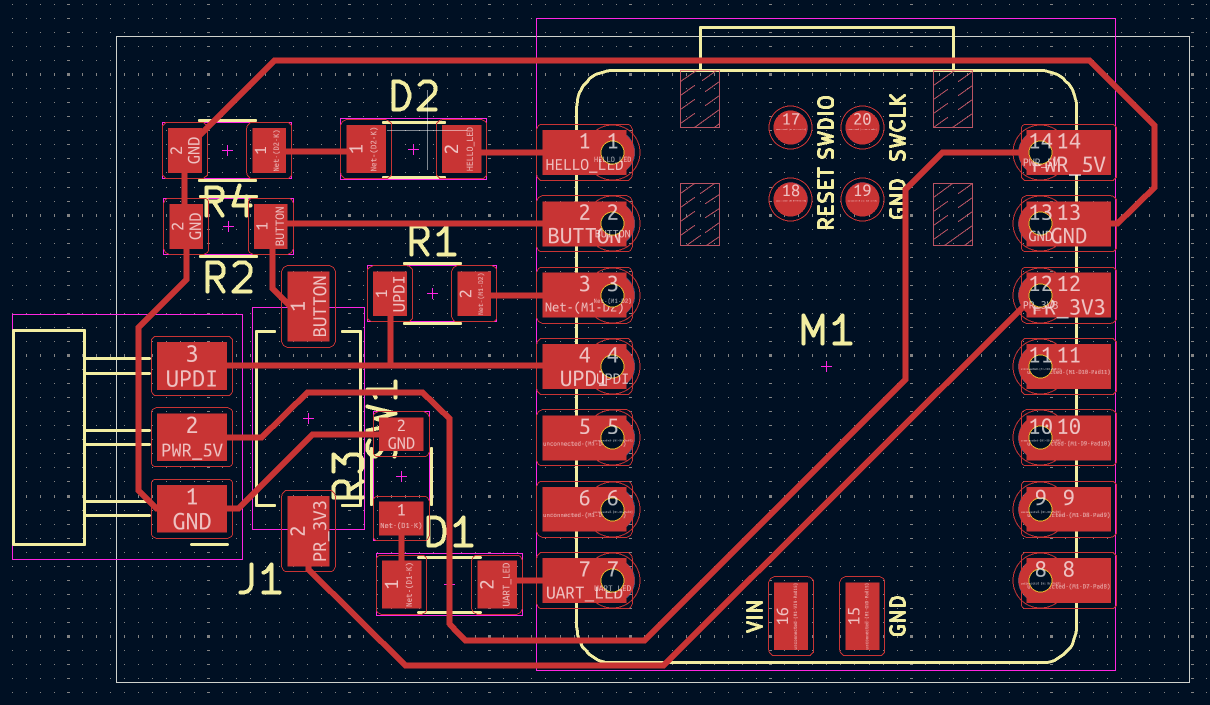
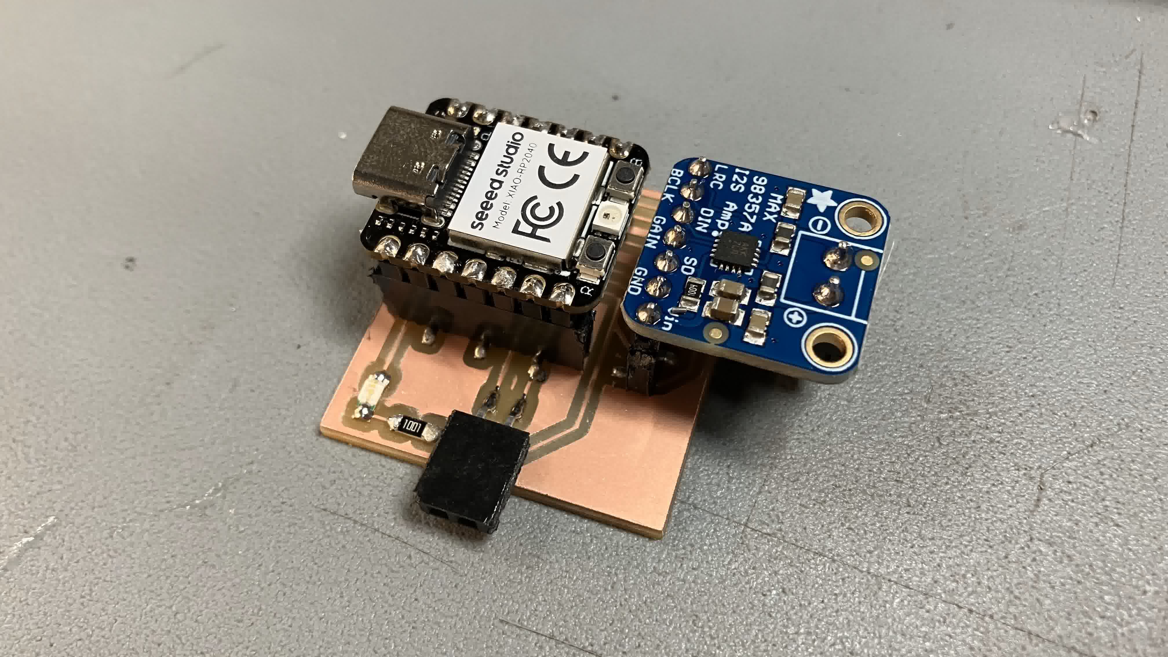
Originally, I had thought about using an AVR128DB32 on the motherboard as well as the daughterboards for the sake of continuity, but then I realized that microcontroller cannot transmit digital audio data through I2S, which is the protocol I intend to use. My idea is for the motherboard to be connected to the daughterboards via I2C, then do internal programming from the keys and breath sensor and then send the digital audio into an amplifier connected to a speaker. So I decided to use a XiaoRP2040 as a microcontroller and a MAX98357A as an amplifier. My board is mainly based on this design by Neil, I just added an LED for troubleshooting and the channels for I2C communication. So the design looked like this:
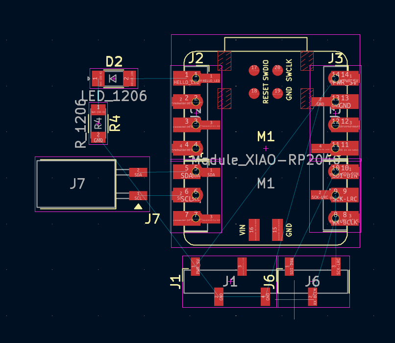
But since I didn't want to solder the Xiao RP2040 directly into the board, I put vertical pin sockets so that I could remove it if needed. So the PCB design ended up lookig like this:
After following the workflow for our in-house production, I got to milling:
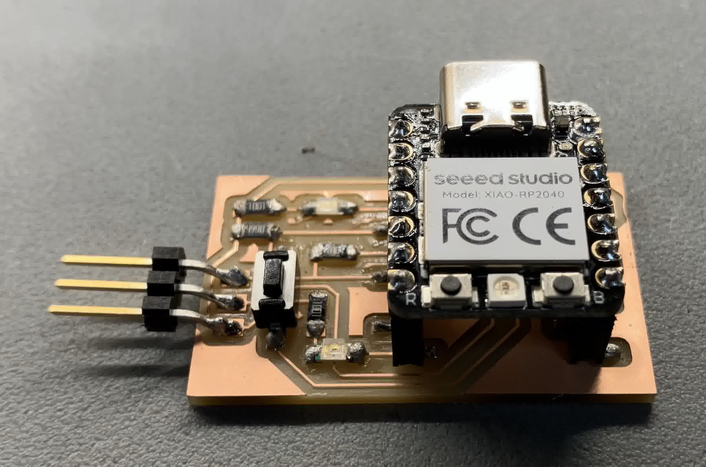
Then I got to soldering the components in, so it looked like this:
Daughterboards
After designing my development board in Week 6 and learning from some mistakes there, I came up with the following schematic for the first daughterboard:
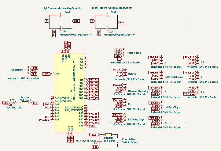
To get to this point in the schematic, I started, as always, by diving deep into the datasheet which is available here. So firstly, I familiarized myself with the microcontroller's pinout:
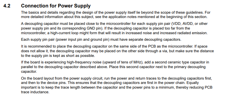
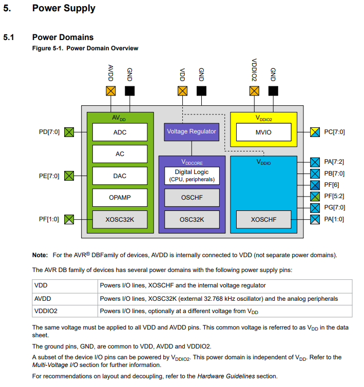
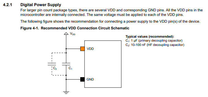
Then, I started with understanding the connection to the power supply better:
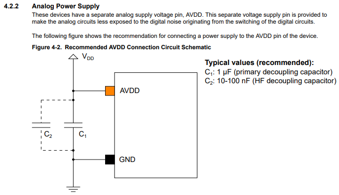
So after understanding how the microcontroller worked in regards to this, I set up the AVDD and VDD connections to power supply, selecting the components in accordance to what the datasheet recommended:
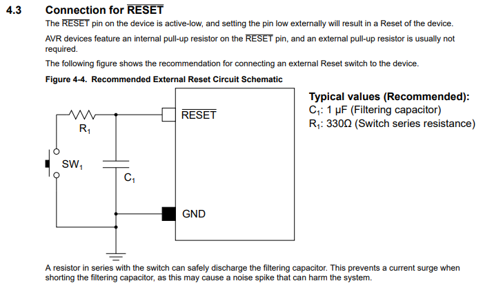
Then, I set up the reset button by selecting the components in accordance to what the datasheet recommended:
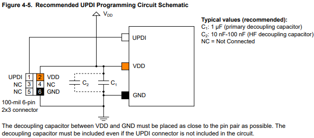
Then, I set up the UPDI programming connector by selecting the components in accordance to what the datasheet recommended:
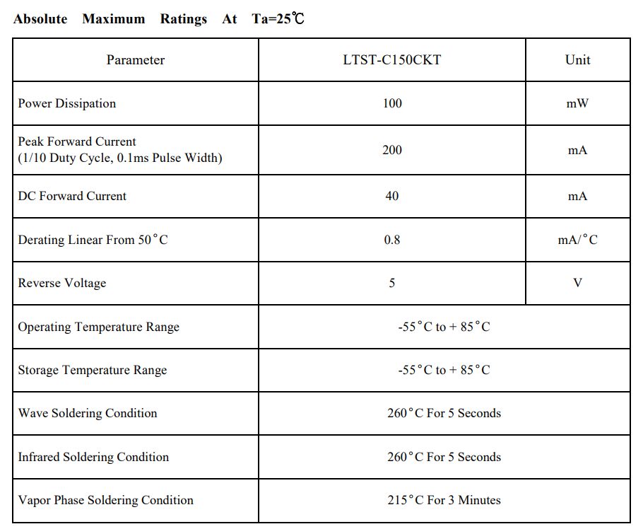
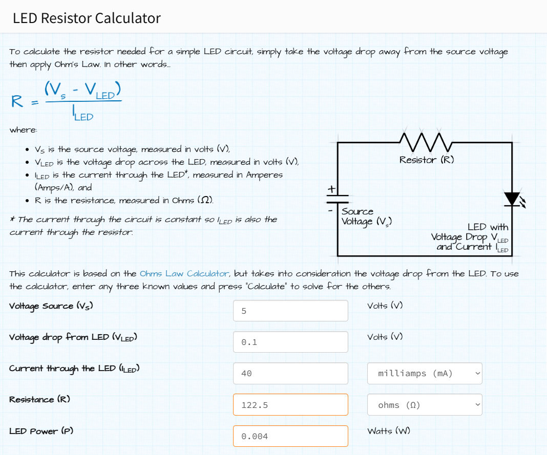
Then, I wanted to add an LED light to the board to make troubleshooting easier for myself. So I looked at the datasheet for the one I chose:
Based on the datasheet, I used this calculator to determine which resistor to use:
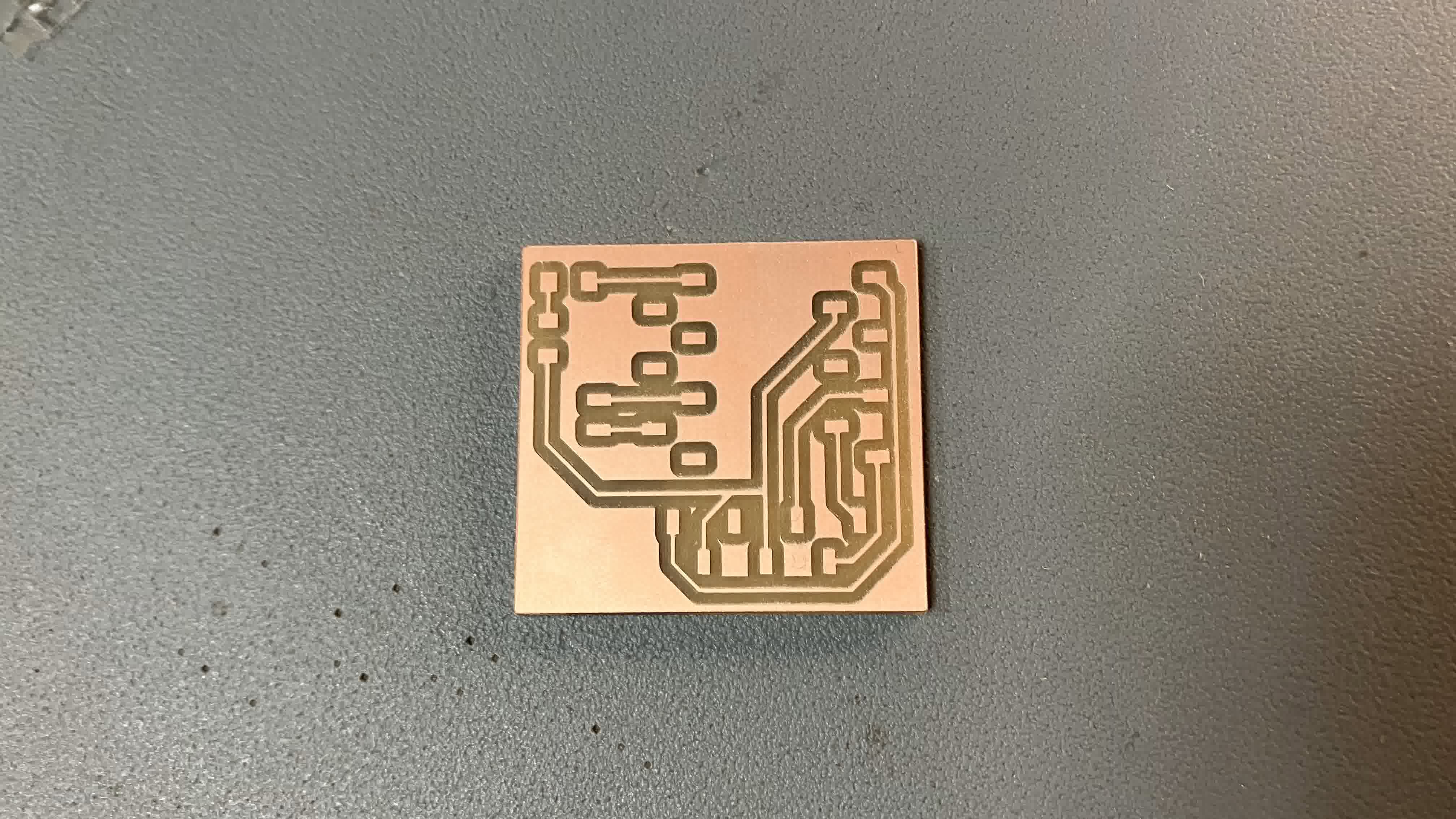
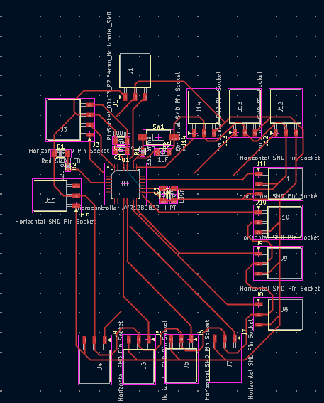
Then, it was time for me to switch over to the PCB editor. Due to our in-house limitations, we cannot have gaps thinner than 0.4mm, so I had to modify some footprints to accommodate this. I decided to have the tracks have a width of 0.3mm, but the ones closer to the microcontroller had to be 0.2 in order for me to be able to produce the PCB in-house in a few weeks. So all in all, the final PCB design looked like this:
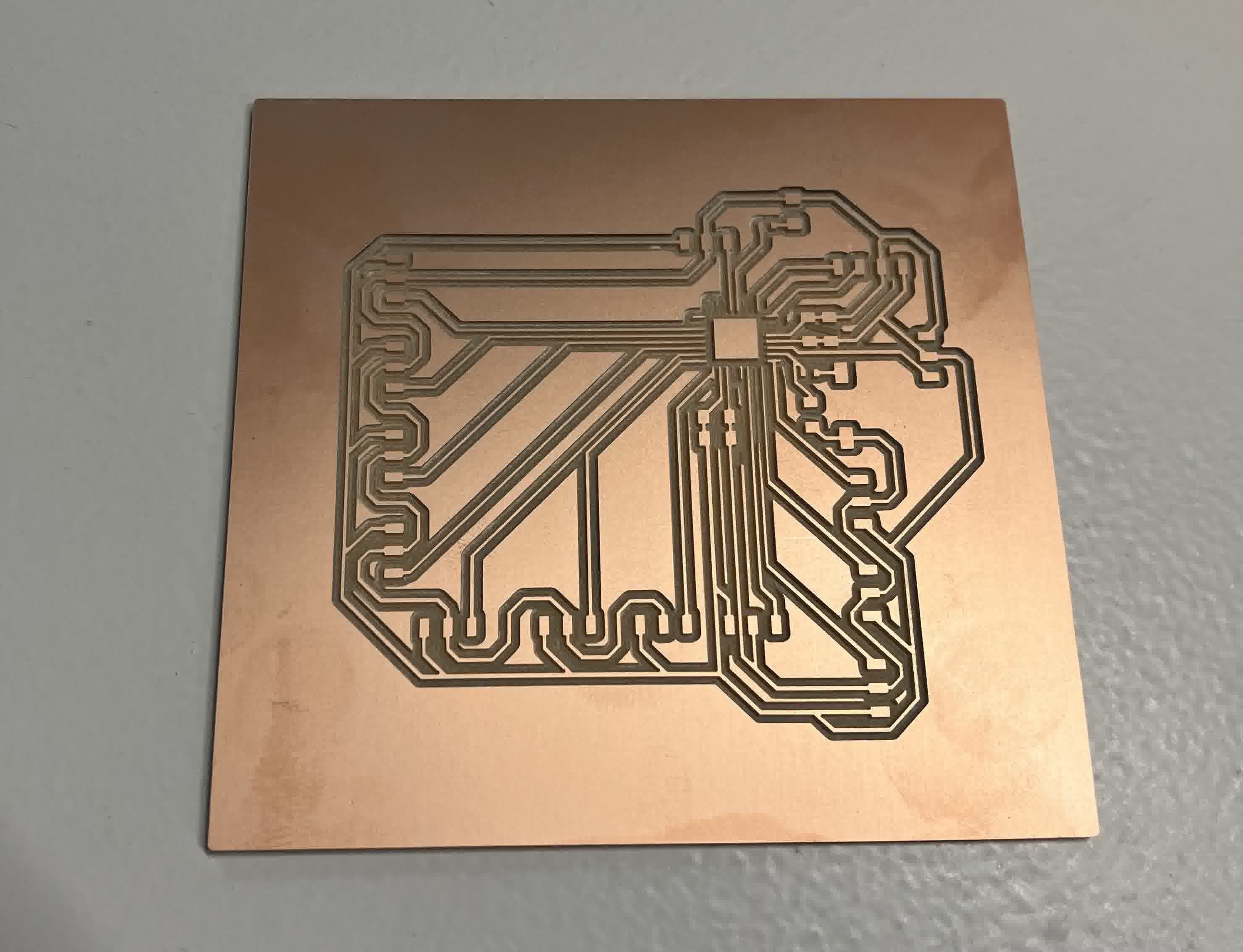
After following the workflow for our in-house production, I got to milling:
And finally, soldering:
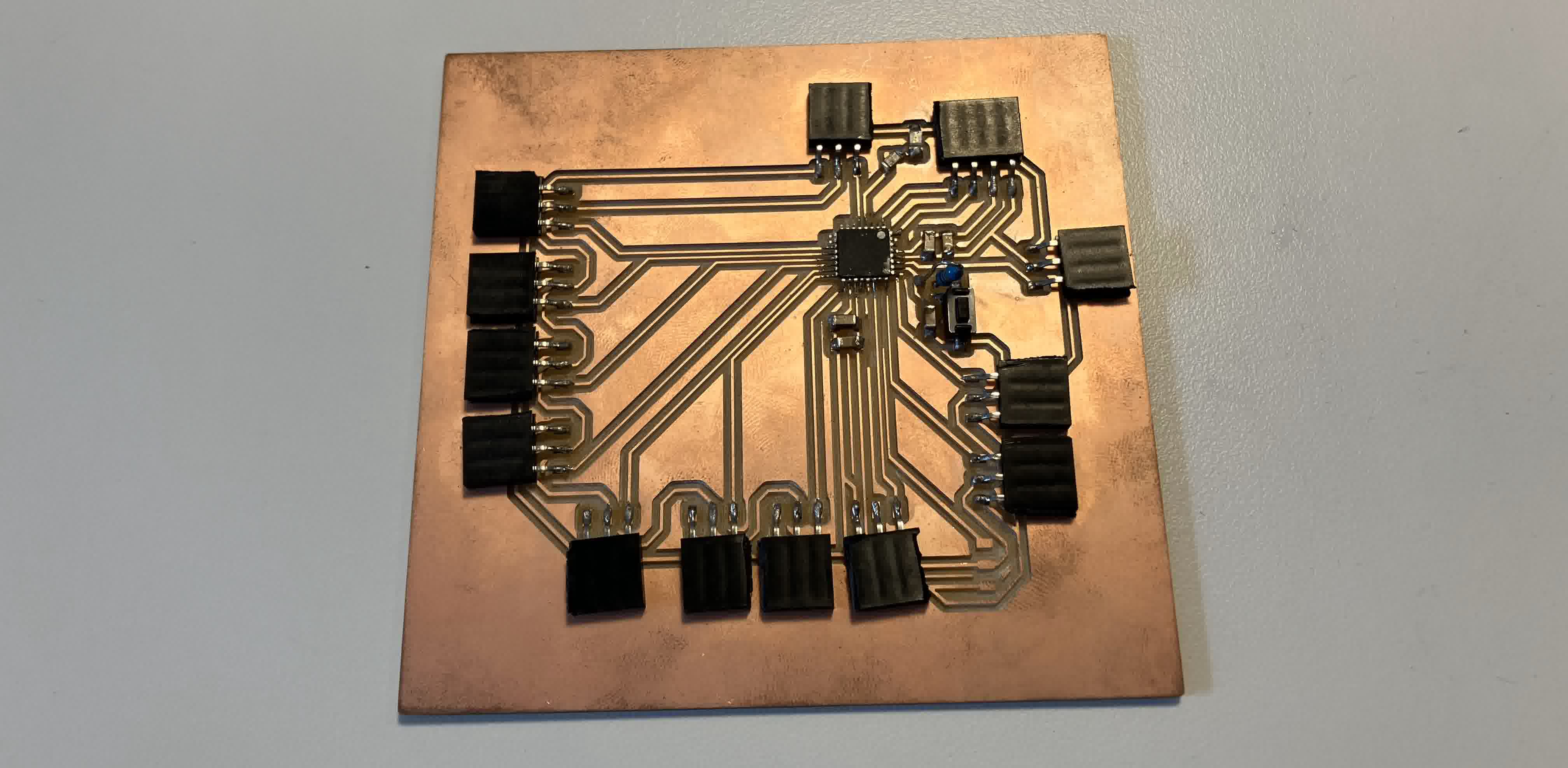
Now, you may see that there is one pin socket connector missing. This is because one of its lines was cut off during the milling process. I still decided to go ahead with this board instead of building another one so that I could use this one for initial testing.
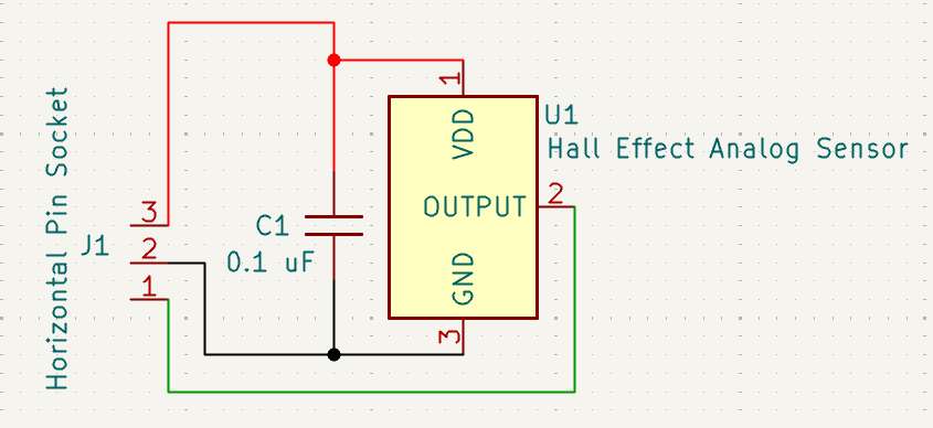
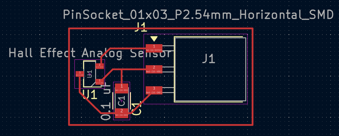
Granddaughterboard
Having the daughterboard ready, I needed the input devices I would be measuring with it, so I designed the general granddaughterboard that each one of the keys would have. The schematic and PCB design looked like this:
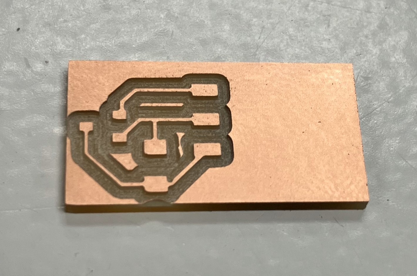
After following the workflow for our in-house production, I got to milling:
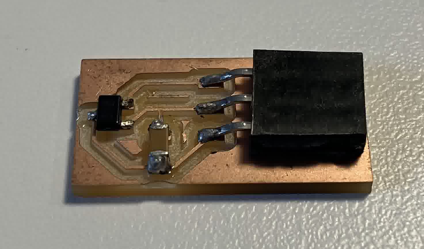
And finally, soldering:
Mechanical Components
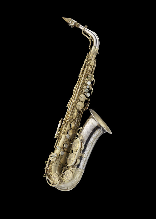
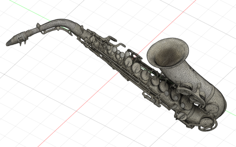
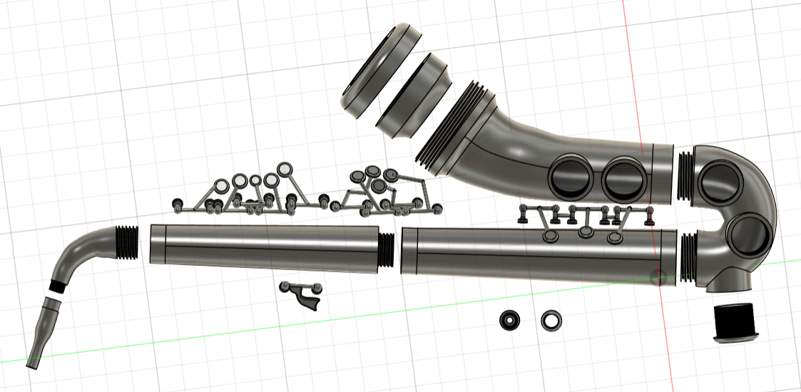
Since I wanted my saxophone to have the dimensions of a real saxophone, I downloaded this 3D model of Charlie Parker's Alto Saxophone from the Smithsonian Institution's Digitization Program Office.
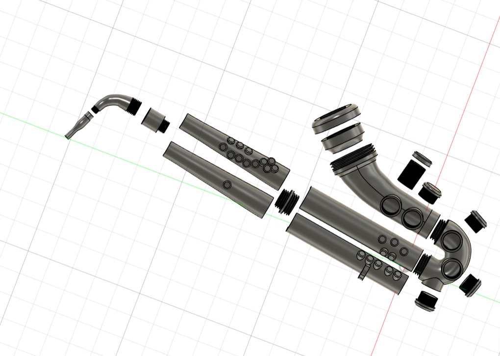
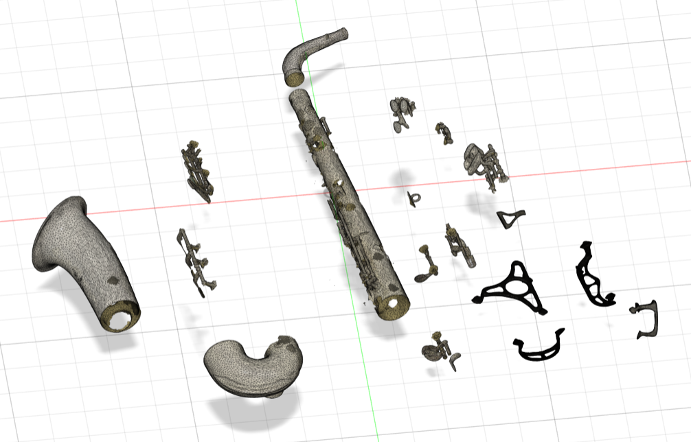
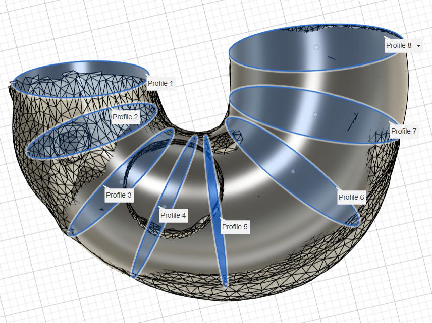
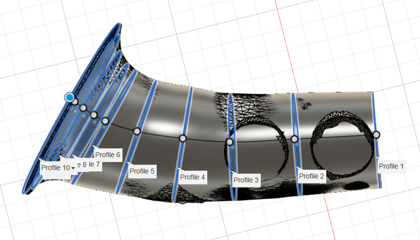
Once I had the mesh design, I exploded it into different pieces because I already knew that due to sizing restrictions I was going to have to print it in pieces:
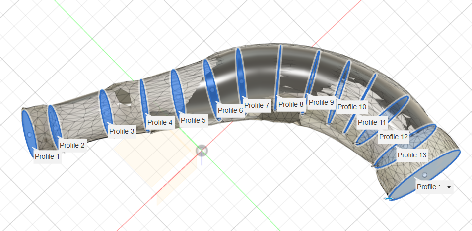
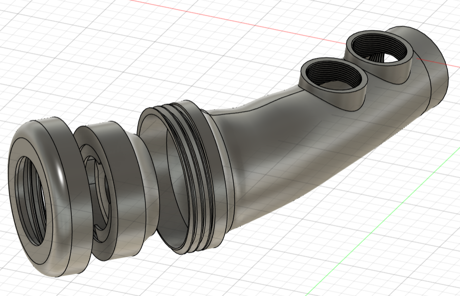
Then I started creating sketches and solid pieces around the mesh parts:
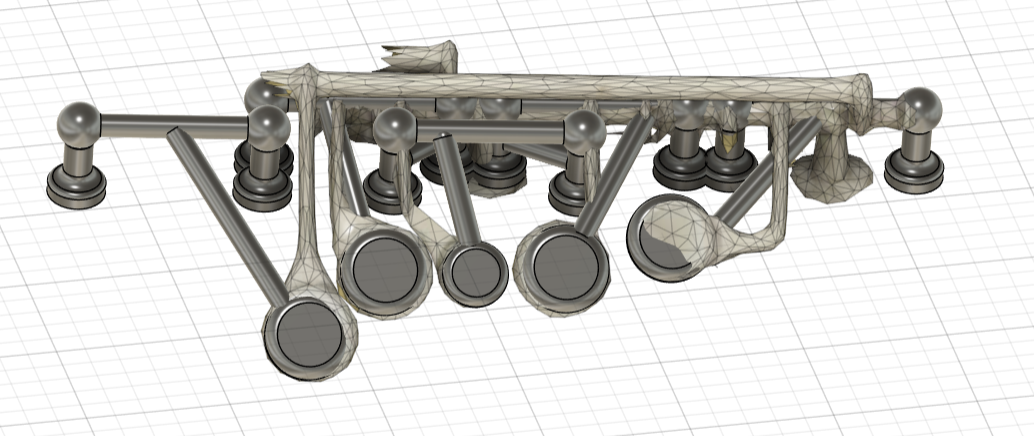
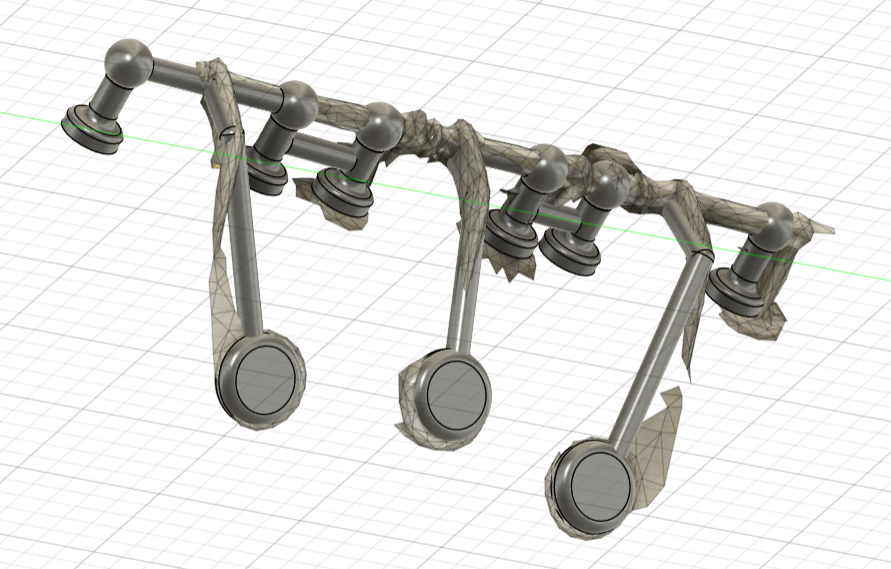
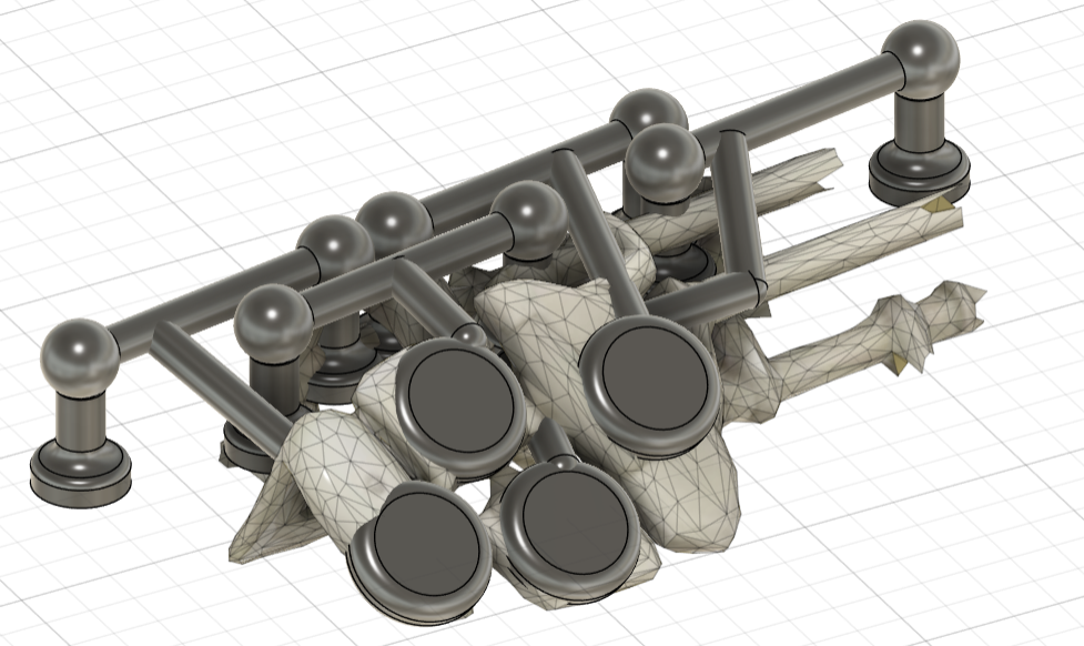
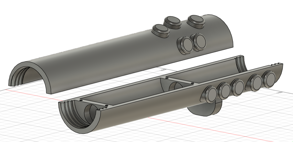
After that I incorporated system integration techniques to make sure all the separate pieces would fit together and could properly house the electronic components:
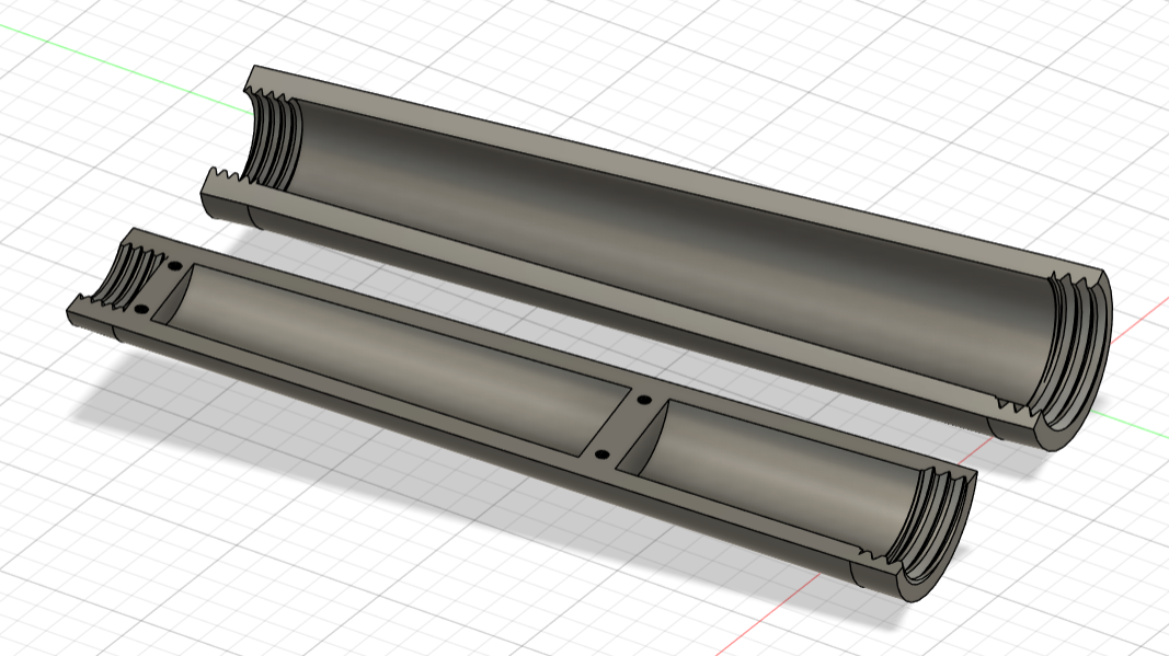
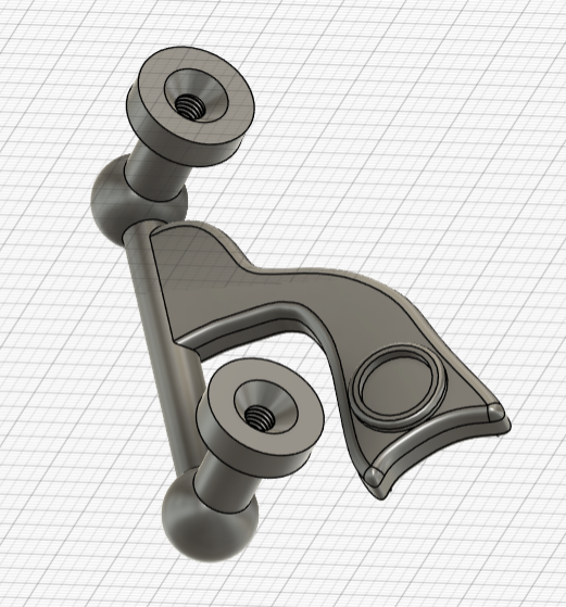
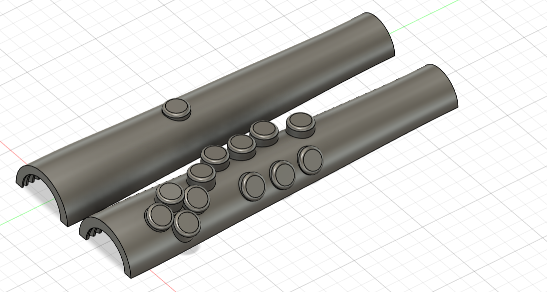
The original plan was to have the keys be the same as on a regular saxophone, but after various iterations and PLA prints, I couldn't get them to maintain structural integrity after multiple uses. Since I was starting to run out of time, I had to make a quick switch and replace the mechanical keys with simple buttons. This meant changing the top and bottom bodies so that they ended up looking like this:
So that the final exploded model of the saxophone looked like this: