Week 6
Electronics Design
Week Outline
- Wednesday: Global Class on Electronics Design.
- Thursday: Local Classes on Choosing Electronics and KiCad.
- Wednesday: Global Review.
Global Class
For this week's global class, Neil started by explaining the different components we will most likely be using and how they work. The he explained the workflow used to design electronic circuits and showed us the different softwares we can use for this process. Additionally, he showed us software we can use to simuate our circuits and equipment we can use to test our circuit after it has been produced.
Local Classes
Unfortunately, I wasn't able to attend classes in person this week due to some health issues. However, the instructors very kindly offered to record them for me to be able to see on my own. So, luckily, I got to learn how to choose electronics and use KiCad from home.
Assignments
1. As a group, use the test equipment in your lab to observe the operation of a microcontroller circuit board.
The documentation of the work we did can be found here.
2. Use an Electronic Design Automation tool to design a development board that uses parts from the inventory to interact and communicate with an embedded microcontroller.
Electronic Design Automation of a Development Board on KiCad
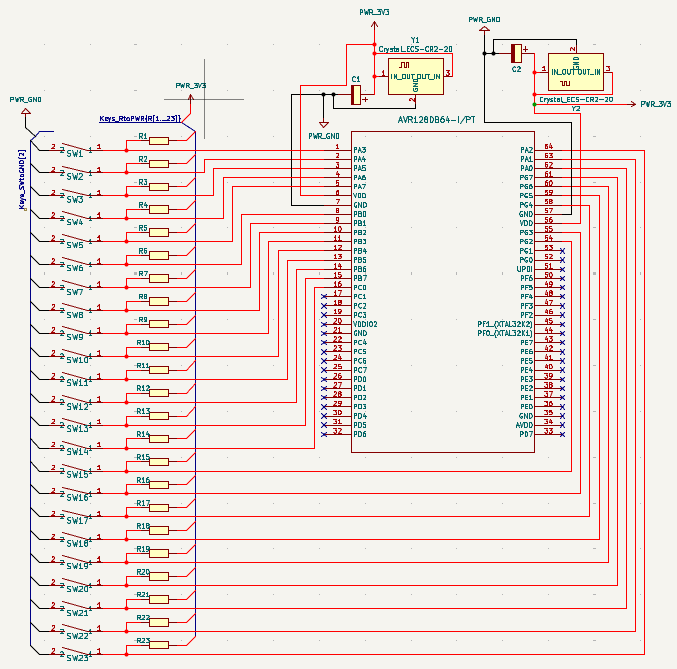
I wanted to design a development board that would allow me to build the foundation for my final project. I knew that I would need 22 analog inputs just for the saxophone's keys, plus the inputs for the breath chamber sensors. So initially, I thought about using the AVR128DB64 microcontroller on a motherboard and having all the inputs go directly into it, like you can see below:
After speaking with Dani, we discussed that a better approach might be to have daughterboard going into the main motherboard so as to simplify things. So instead of having my final project be a single pcb with a ridiculous amount of inputs, I decided to have the left hand keys go into one board, the right hand keys go into another board, the breath chamber sensors go into another board, and have all 3 of these boards go into the main motherboard. So instead of using the AVR128DB64 microcontroller, I decided to use the AVR128DB32 microcontroller for all 4 boards.
However, before going straight into designing the boards for my final project, I wanted to do this development board as kind of a middle point, so as to get to know the microcontroller better and be able to test out different things with it. So my first design was the next one:
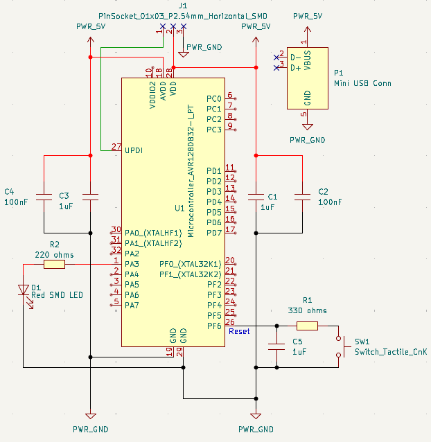
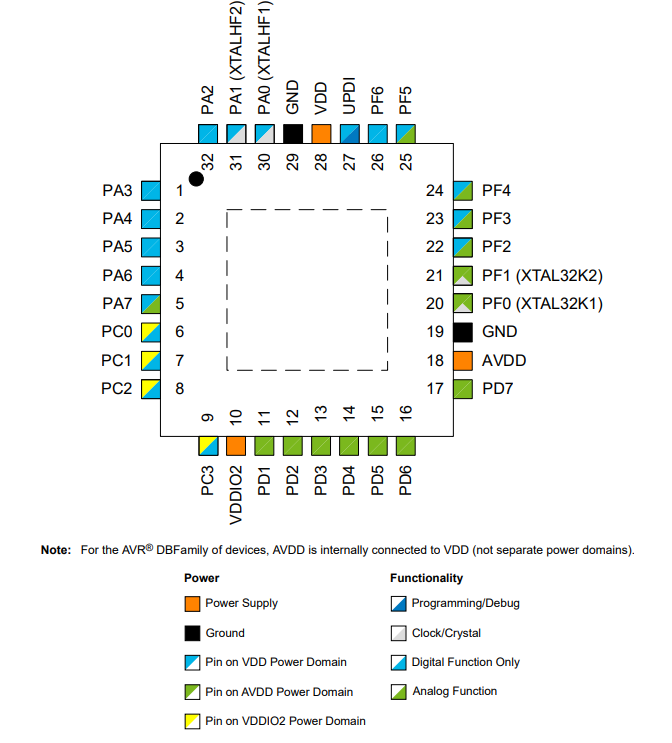
To get this, I started, as always, by diving deep into the datasheet which is available here. So firstly, I familiarized myself with the microcontroller's pinout:
Then, I started with understanding the connection to the power supply better:
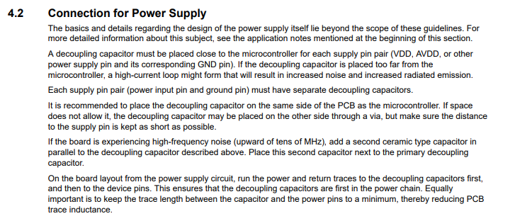
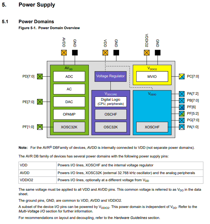
So after understanding how the microcontroller worked in regards to this, I set up the AVDD and VDD connections to power supply, selecting the components in accordance to what the datasheet recommended:
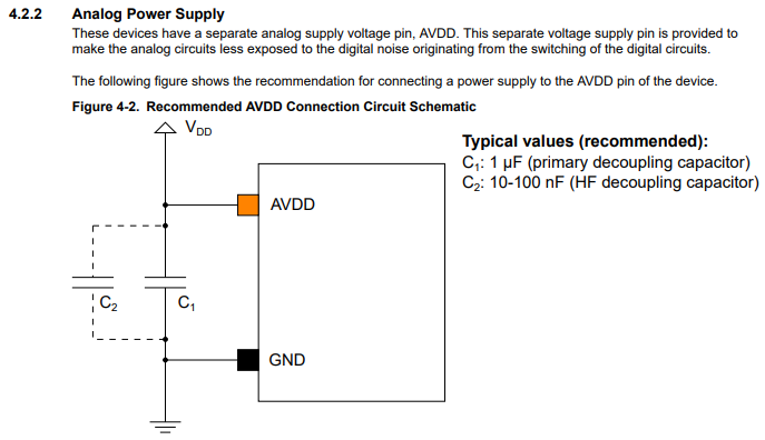
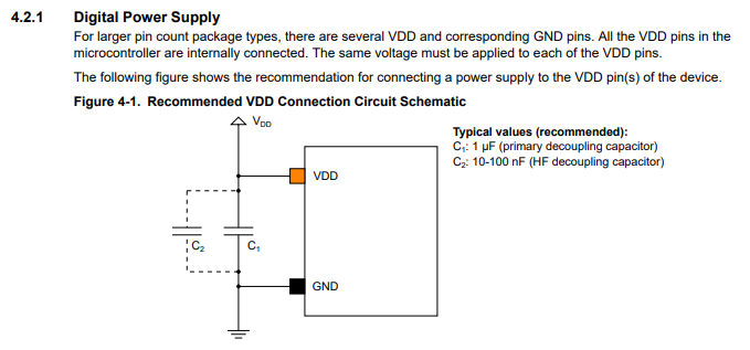
Then, I set up the reset button by selecting the components in accordance to what the datasheet recommended:
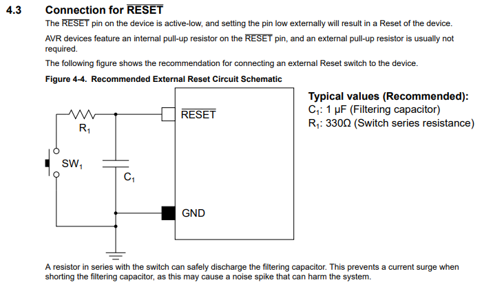
Then, I set up the UPDI programming connector by selecting the components in accordance to what the datasheet recommended:
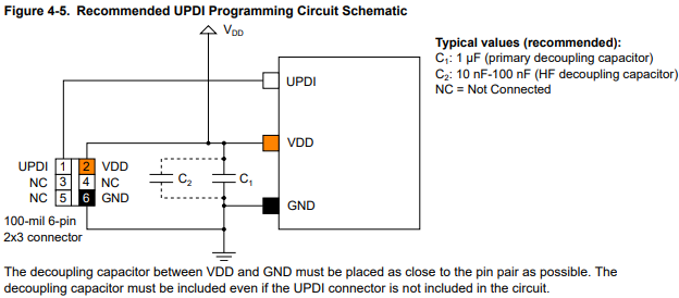
Then, I wanted to add an LED light to the board to make troubleshooting easier for myself. So I looked at the datasheet for the one I chose:
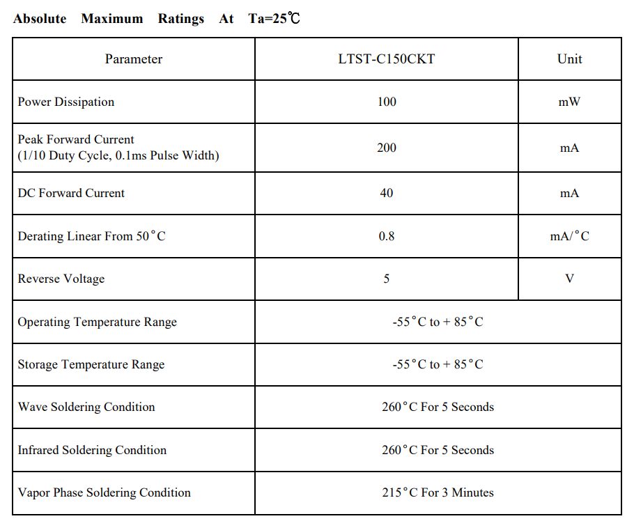
Based on the datasheet, I used this calculator to determine which resistor to use:
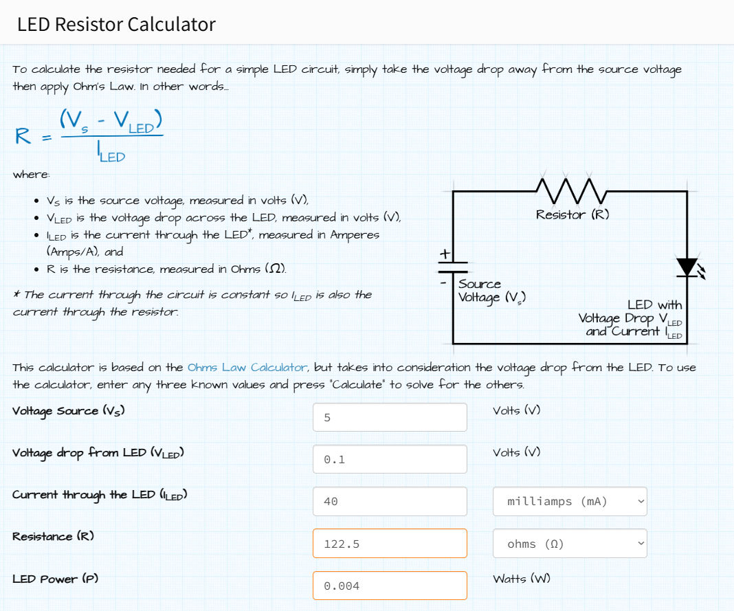
Then, after giving it some thought, I decided that since this was a development board, that I wanted to give myself the option to use the option for a secondary voltage input, so I went back and familiarized myself with how to set up the VDDIO2 connections to power supply, selecting the components in accordance to what the datasheet recommended:
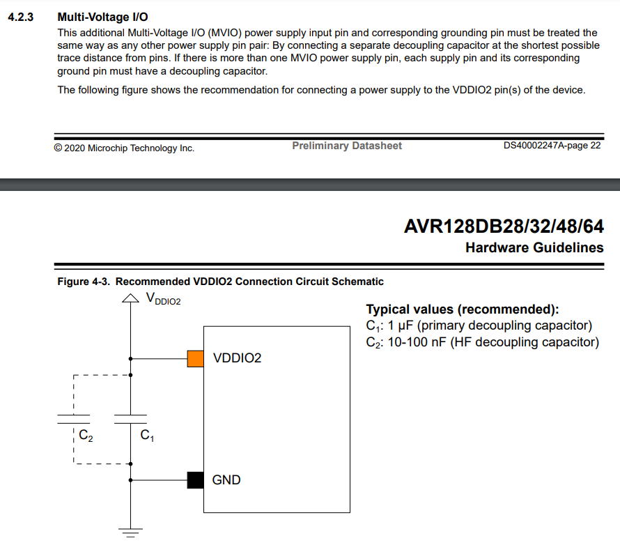
I also decided to add a button to have for testing. I made enough holes for me to solder pins so that I can utilize every single pin on the microcontroller if I wish to. All of this led me to the following design:
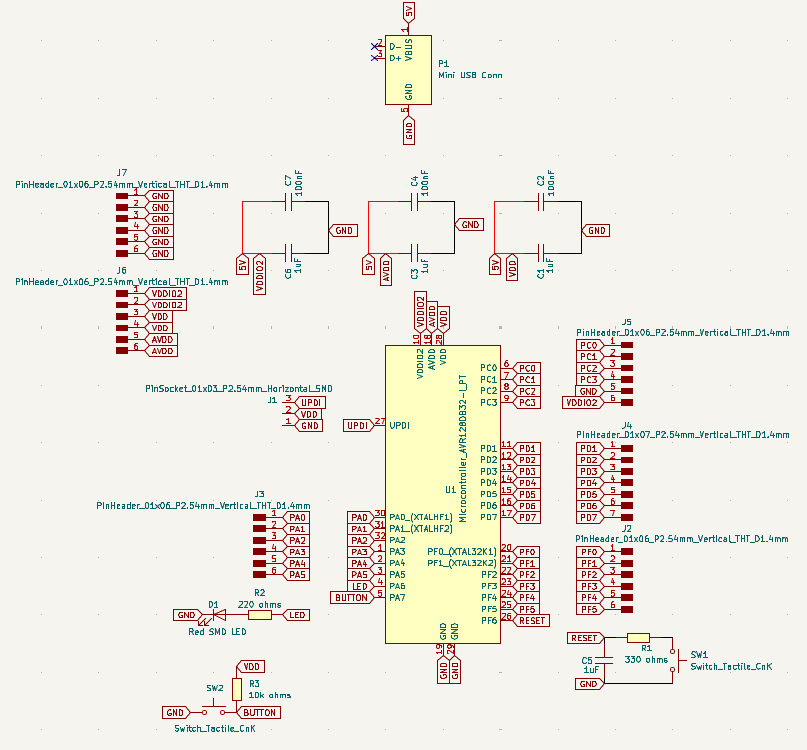
The schematic can be downloaded here.
Then, it was time for me to switch over to the PCB editor and get cracking. I decided I wanted the board to have the shape of a musical note, so I did the nesting in accordance to this concept. However, due to our in-house limitations, we cannot have gaps thinner than 0.4mm, so I had to modify some footprints to accommodate this. I decided to have the tracks have a width of 0.3mm, but the ones closer to the microcontroller had to be 0.2 in order for me to be able to produce the PCB in-house in a few weeks. So all in all, the final PCB design looked like this:
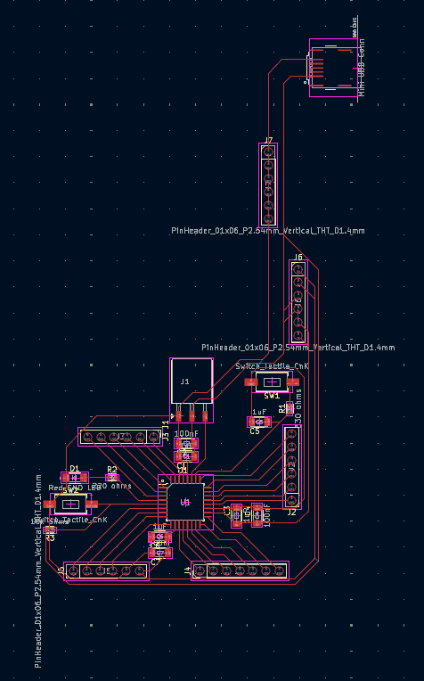
The schematic can be downloaded here.
The Kicad project can be downloaded here.