Week 12
Mechanical Design and Machine Design
Week Outline
- Monday: Introduction to Mechanics Local Class.
- Wednesday: Global Class on Mechanical Design and Machine Design.
Global Class
On this week's Global Class, Neil started by explaining the basic principles involved in mechanical design. Then he talked about different components and mechanisms that can be used in machines. He finished by talking about machine design, and gave us a lot of examples of different machines in general and different machines that have been previously built for this specific assignment.
Local Class
On this week's Local Class, Dani and Miguel introduced us to the basics of mechanics. They explained basic components and principles. Then we walked around the IAAC workspace and looked at different machines, trying to analyze why they were designed the way that they were and seeing how they work.
Group Assignment
This week's group assignment consisted of (1) designing a machine that includes mechanism+actuation+automation+application, (2) building the mechanical parts and operating it manually, and (3) actuating and automating the machine. We decided to build this CNC Wire Bending Machine and add our own twists to it.
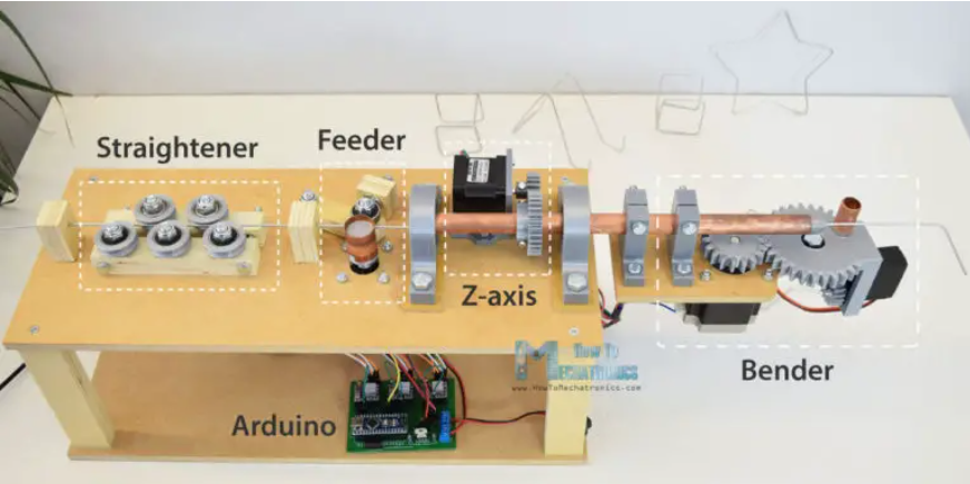
The complete documentation of the work we did can be found here. Our machine ended up looking like this:
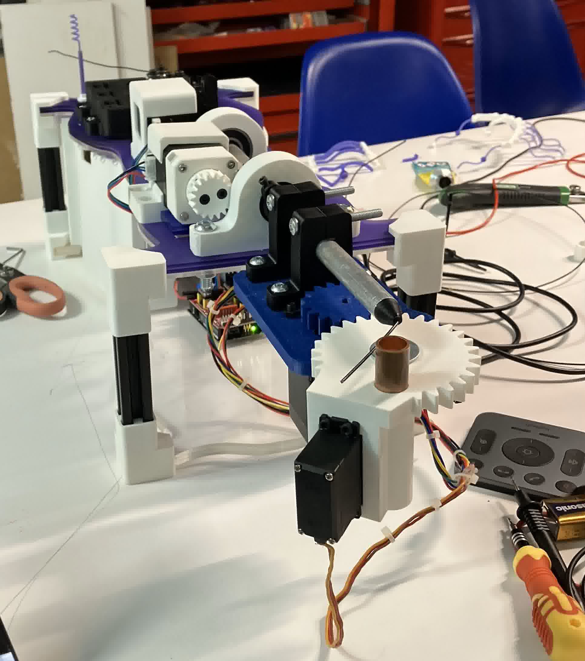
Since we are 6 people, we divided ourselves to divide and conquer. We had some people working on the mechanical design and assembly, some people working on the programming, and some people working on the electronics.
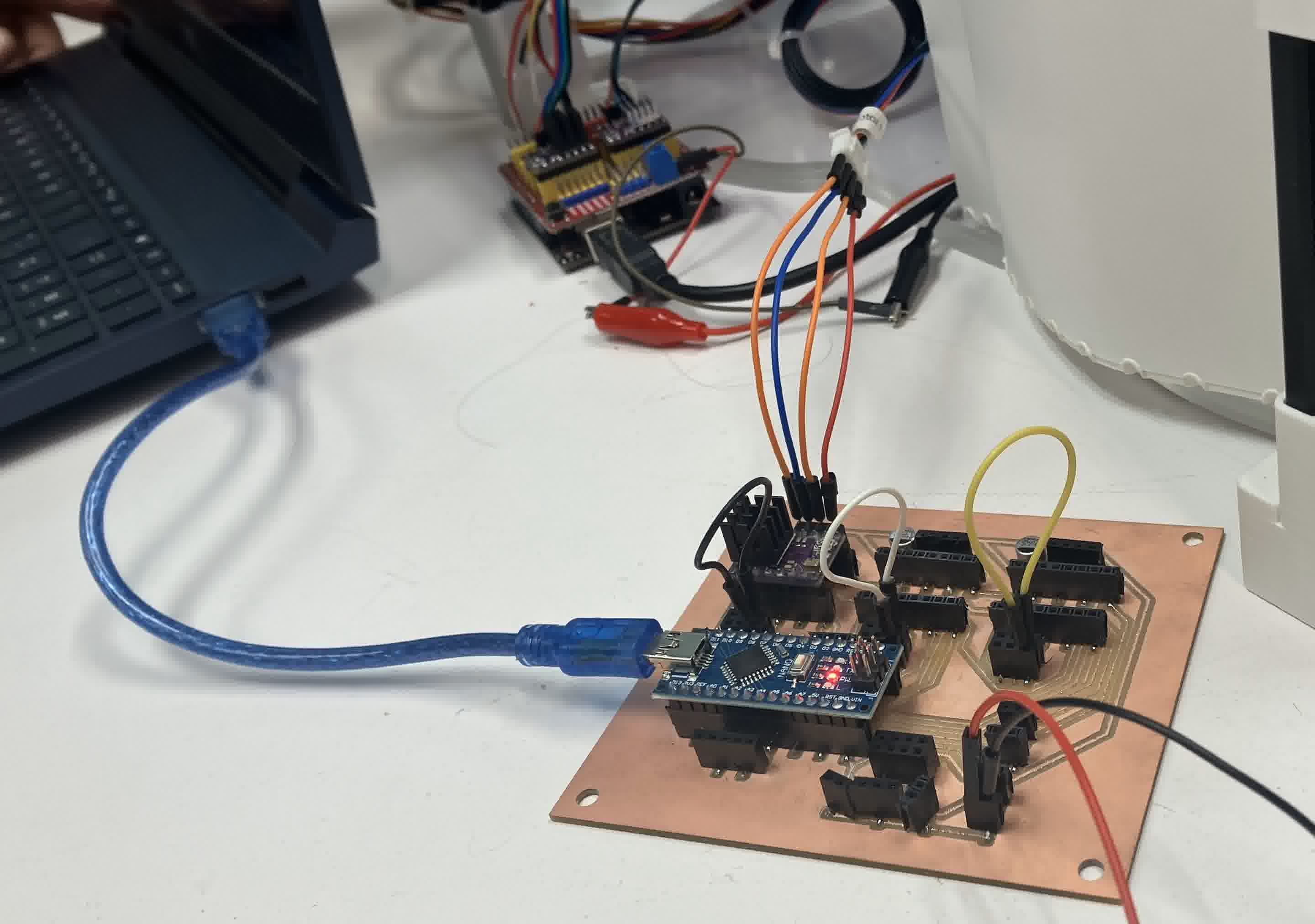
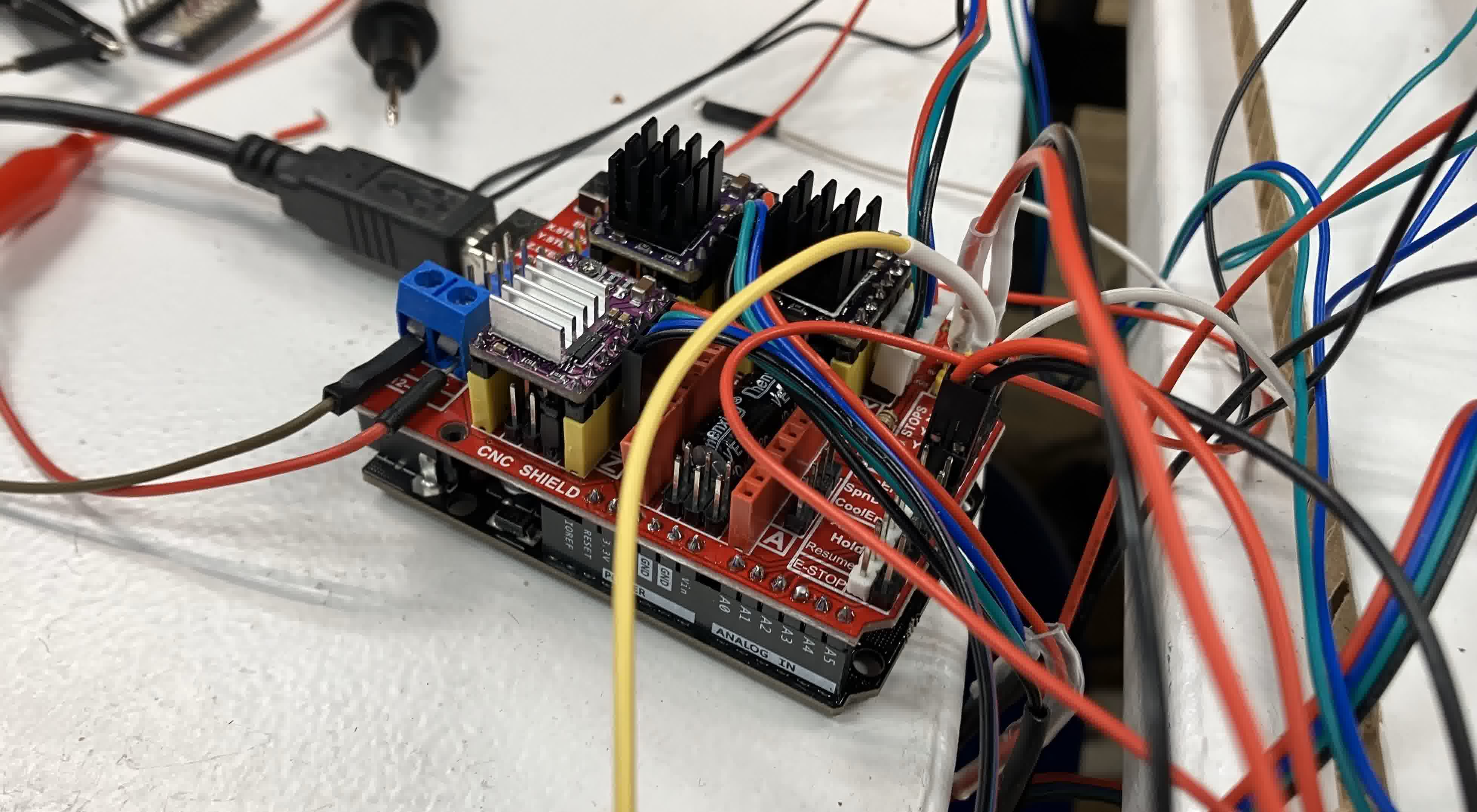
I was part of the group working on electronics. At the beginning, the guys started prototyping the electronics with a CNC shield. However, as you can see below, this was very messy. So my job was to replicate the original project's PCB in a way that we could produce it in-house, using components that we already had in the Lab. The purpose of this was so that we could have a one-sided PCB that we could mount on the bottom of our machine in order to tidy up the electronics on the assembly.
My workflow consisted of:
- Accessed the original project's PCB design files to use as reference.
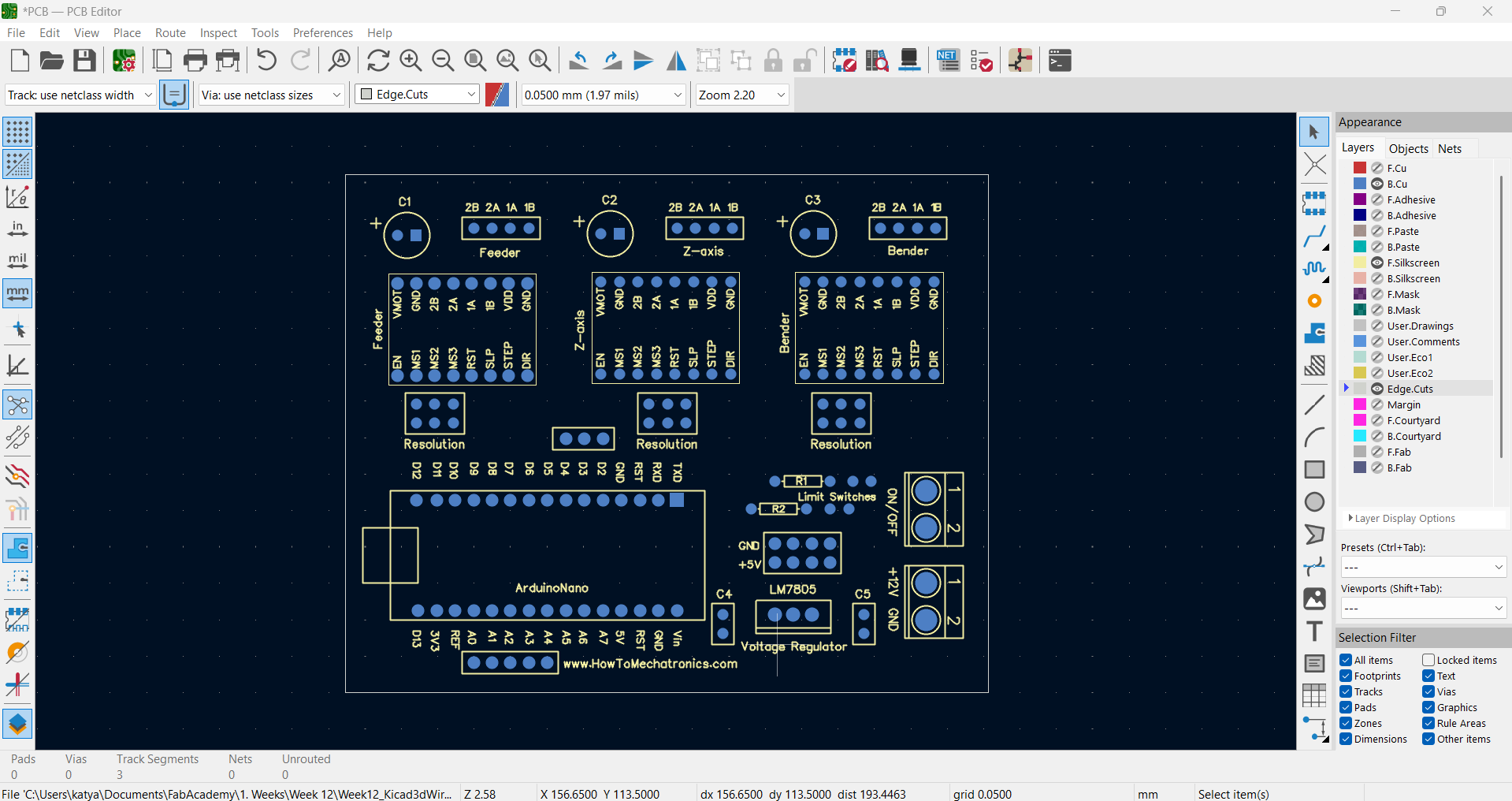
- Created a Kicad Project and created the following schematic (which can be downloaded here)
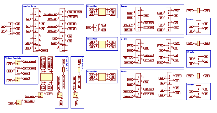
based on the original PCB's design
- Downloaded the original project's Gerber Files that were used for the PCB production. The zip folder with the files can be downloaded here.
- Created a Subdirectory on the project from the file manager called "Gerbers" and copied all the downloaded gerber files into it. Opened the gerbview for the project within kicad.
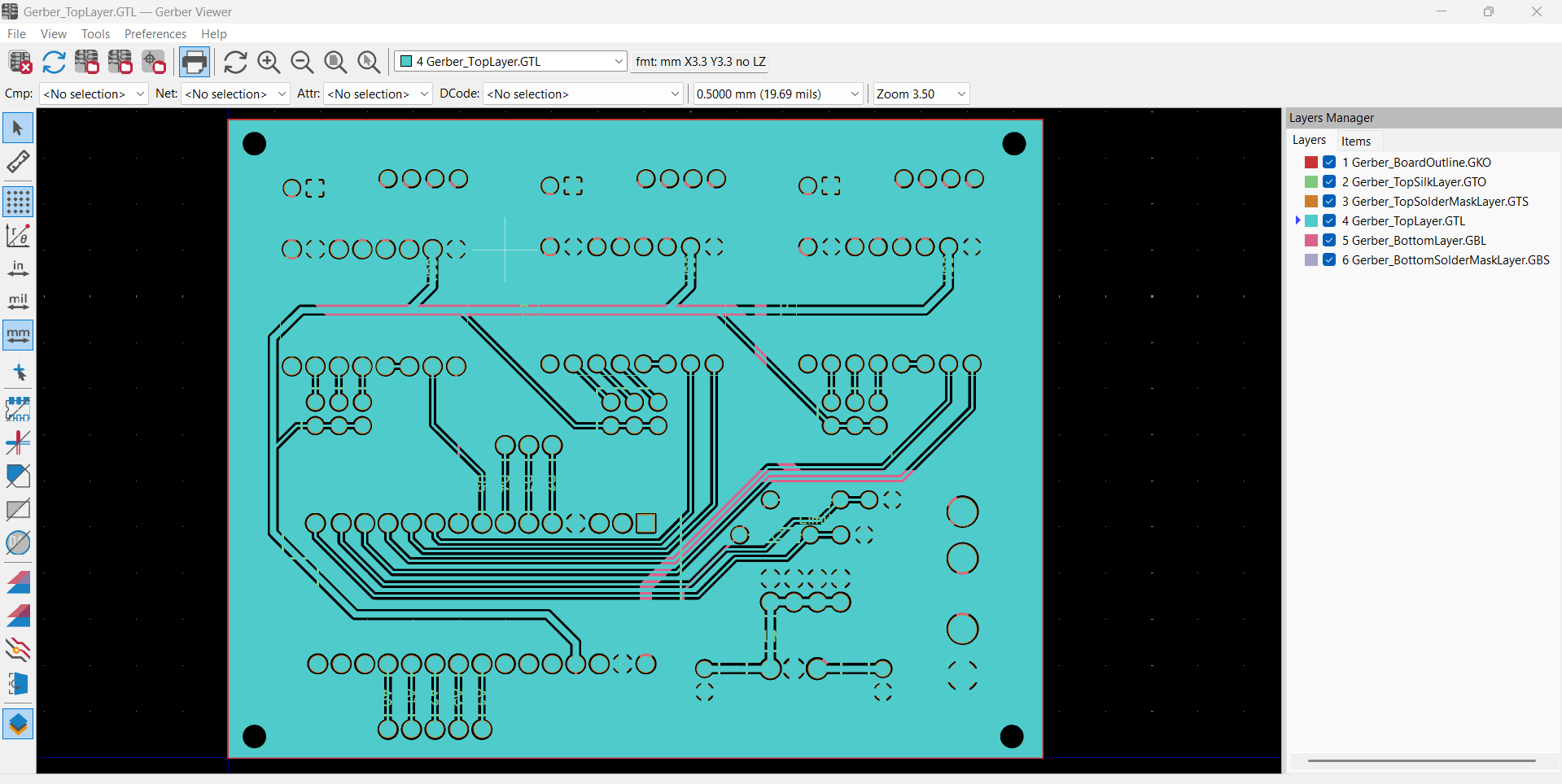
- Selected File > Export to PCB editor and created a pcbnew file off of the original gerber files. Opened the file on the PCB viewer.
- Edited the file so that only the layers that I needed were visible. I was just interested in the physical delimitations of the components in the original PCB, so that I could then overlay my components on them making sure everything fit properly.
- Plotted the visible layers as an SVG. The SVG can be downloaded here.
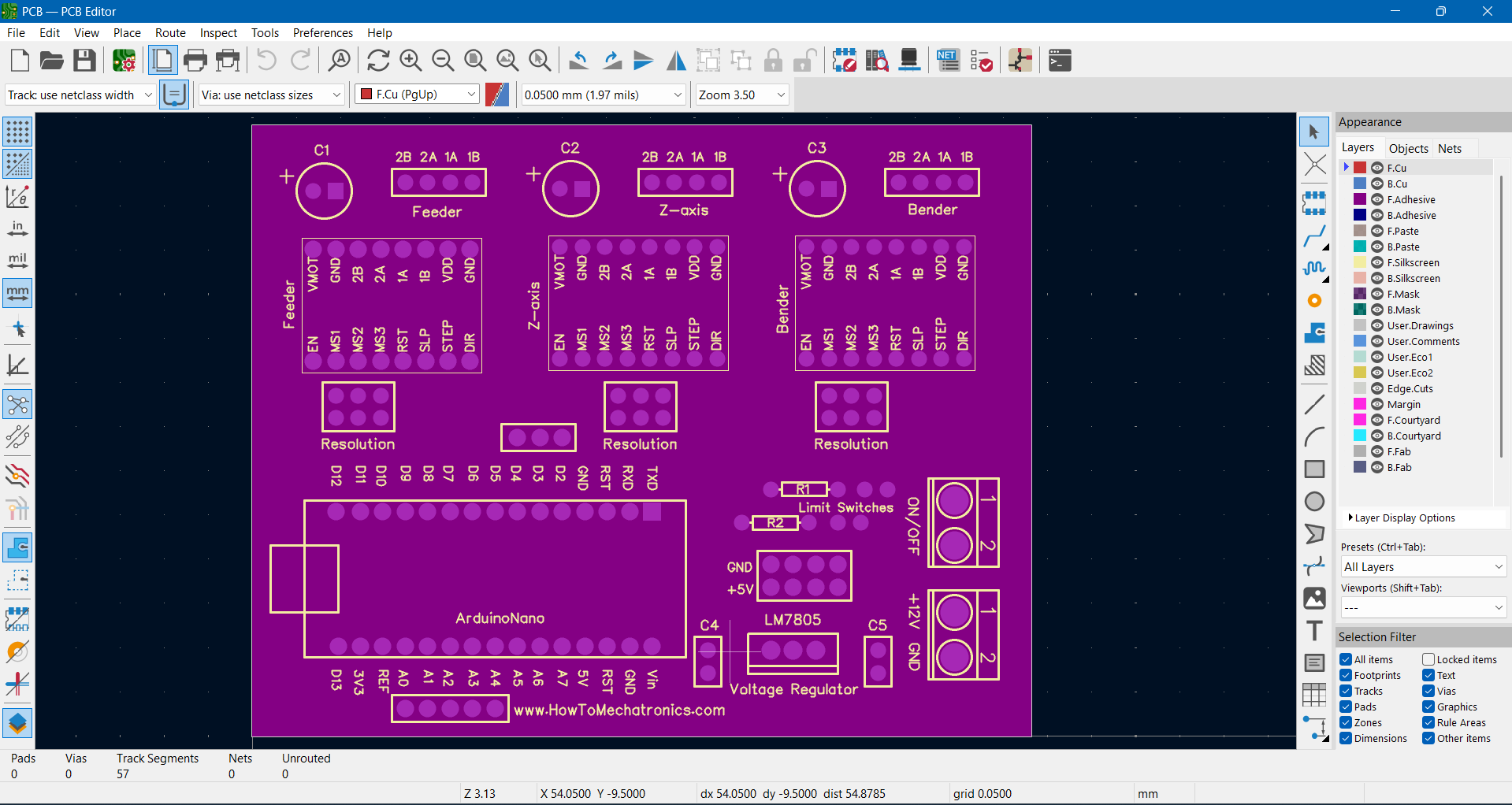
- Created a new PCB file for the project.
- In "File", selected Import > Graphics, and selected the SVG for the layers.
- Overlayed the components from my schematic that needed to have specific dimensions on top of the Graphics
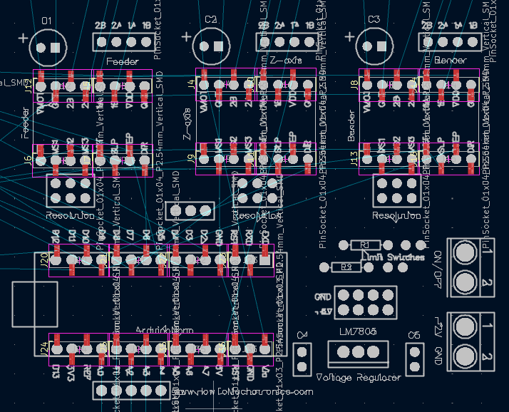
- Deleted the graphics to reduce any chances of confusion for myself.
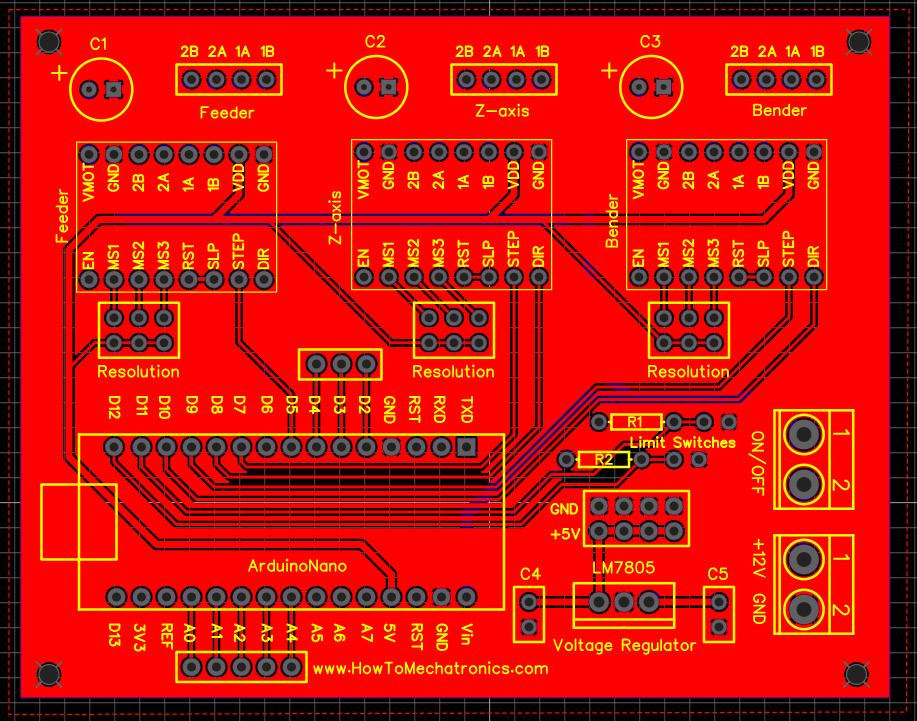
- Finished the components nesting and ran the traces between components by using the original PCB design as reference. Added an edge for the board and holes for screws.
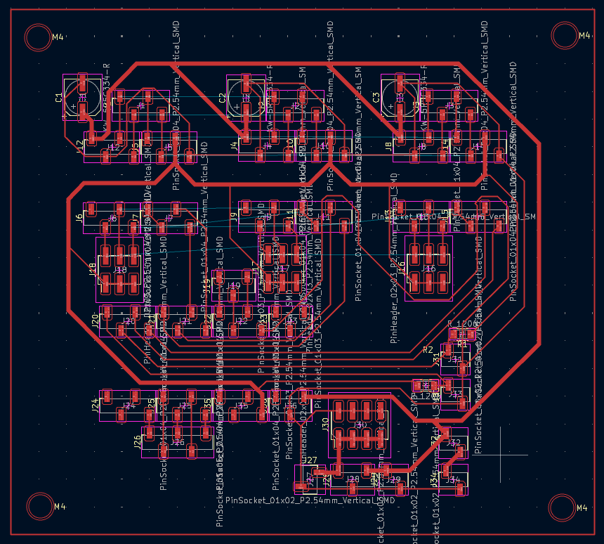
The entire Kicad Project can be downloaded here. - Prepared the files for production (The layers can be downloaded here and the MODS can be downloaded here) and milled the PCB by following our established workflow for in house production
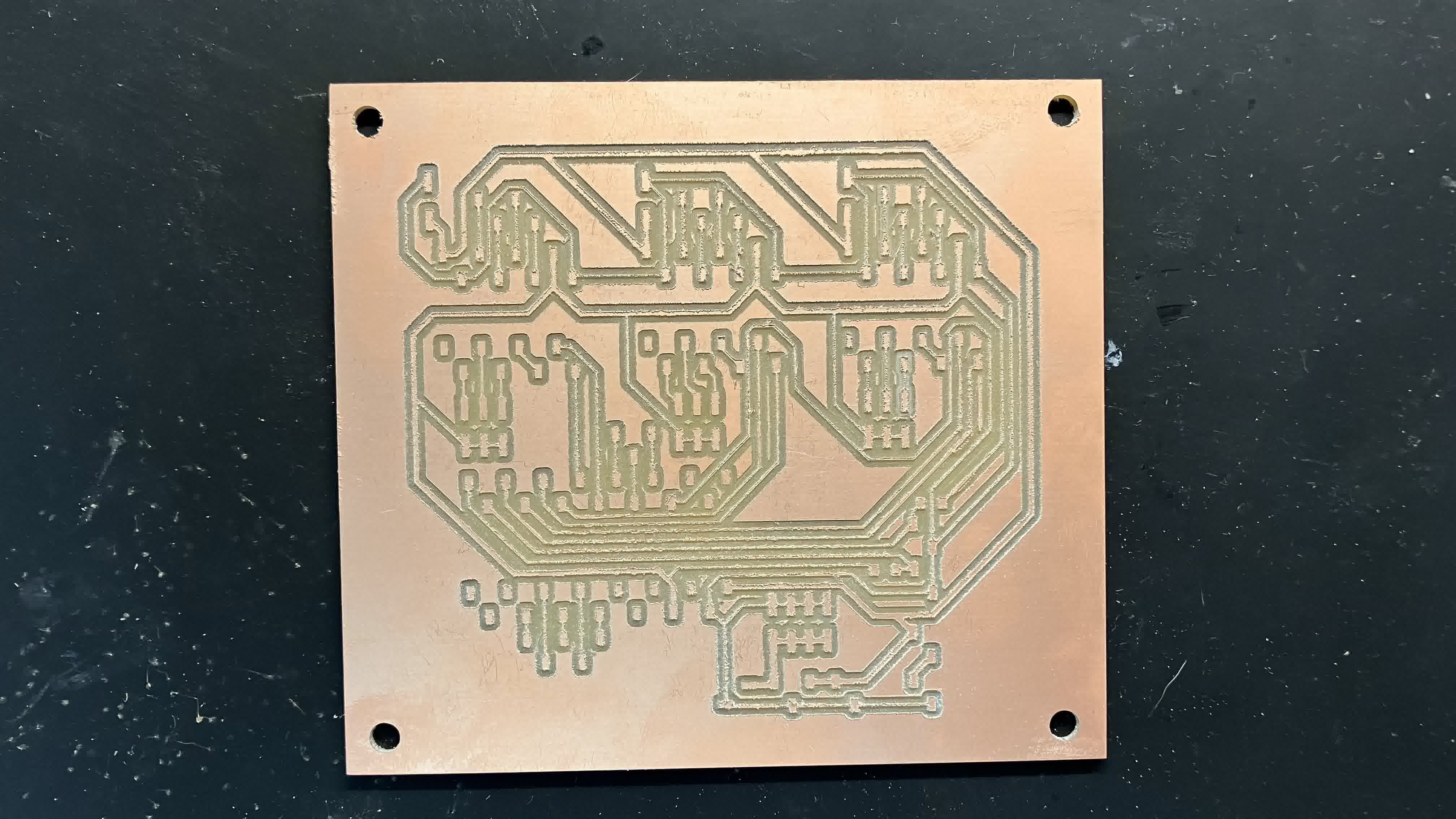
The traces weren't perfect, but they were good enough for an initial prototype. - Soldered the connectors and capacitors into the board
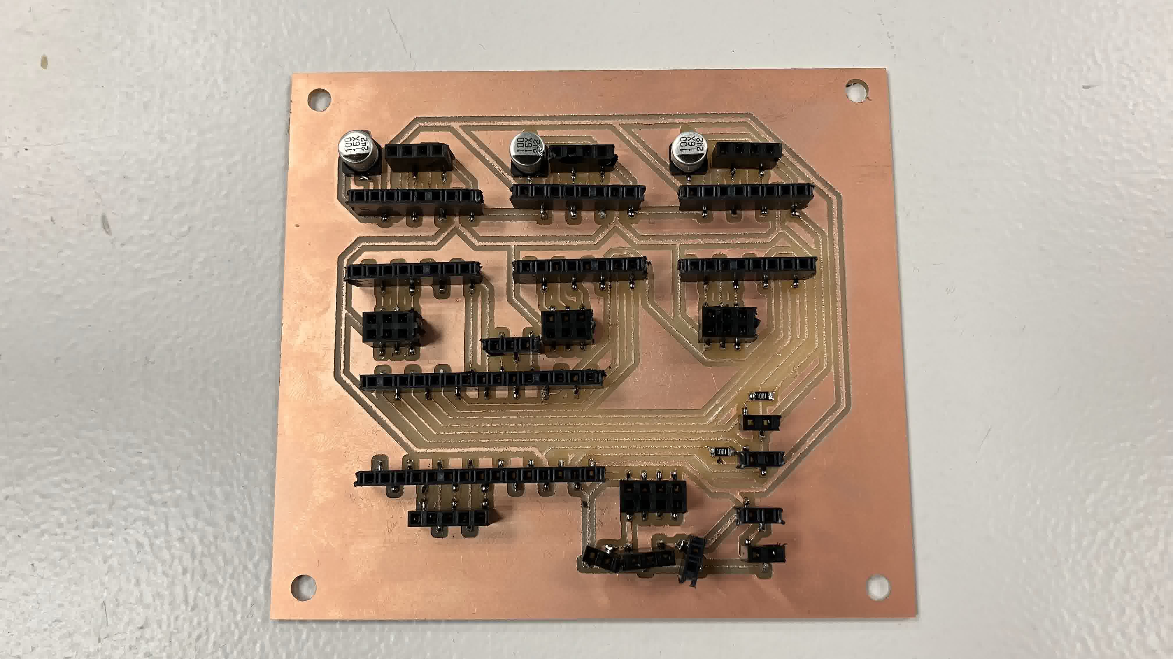
- Passed it on to the guys who started with the testing