8. Electronics Design
Assignments Overview
Here is the list of individual assignments given by the instructors. As for the Group Assignment, please see the Group Assignment page on the FabLab Kannai website:
  > Use an EDA tool to design a development board to interact
     and communicate with an embedded microcontroller,
     produce it, and test it
  > [Extra Credit] Try another design workflow
  > [Extra Credit] Design a case for it
  > [Extra Credit] Simulate its operation
EDA: Electronic Design Automation
How I Responded
In the Global Session on Wednesday, March 13, KiCAD was featured in most detail. However, I decided to go for Fusion Electronics instead. That is because I had already installed Autodesk EAGLE but had not operated much. EAGLE will soon be integrated to Fusion Electronics.
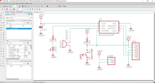
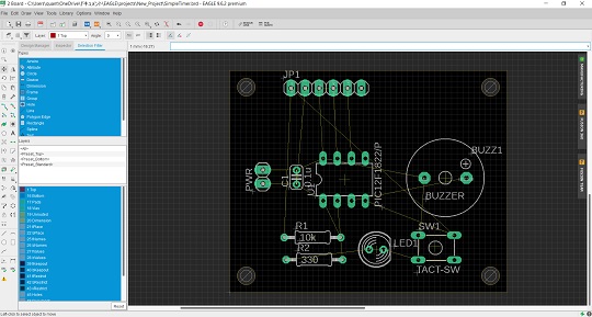
We had a local session on Saturday, March 16 at FabLab Kannai. Before we learned how to design a board with Fusion Electronics in the local session, I personally spent time preparing myself for EDA with EAGLE and a tutorial book written in Japanese. In the preparatory practice, I designed a board for a simple timer.
General Workflow of the EDA Design Process
Here is a flow of the EDA design process I have learned based on the case of EAGLE. As the Autodesk Fusion has been built on the same platform, most of the workflow is almost similar to the one described herewith for EAGLE:
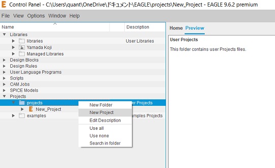
1. Create a New Project
Once you open the program, create a new project folder in the local directory.
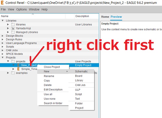
2. Schematic Design
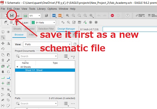
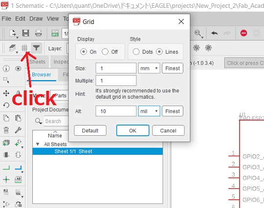
2-1. Activate the Schematic Editor: In the case of EAGLE, if you right-click the new project folder, you can select a new schematic. Once the schematic window is open, you had better save the file first. Change the grid setting by clicking the “Grid” icon. For placing lines or dots on the schematic window, 1mm grid is more helpful.
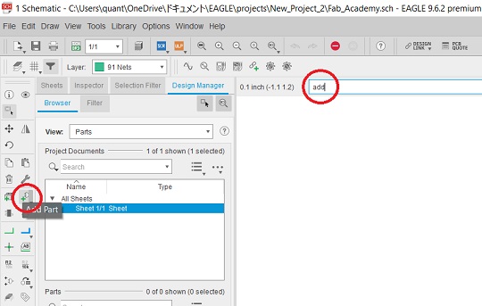
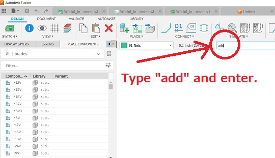
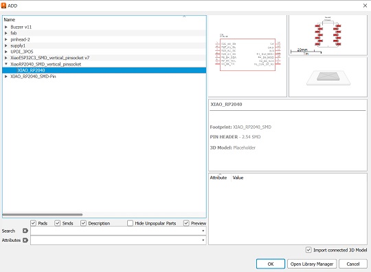
2-2. Add Components: By either typing “add” or clicking the “Add Parts” icon, you open the “Add Parts” dialogue window and select the components you want and place them on the schematic sheet. Once you place them, cancel the further operations by pressing the ESC key. You can also delete the components by pressing the delete key or clicking the trash icon. Move and rotate the components on the schematic sheet if you deem it necessary.
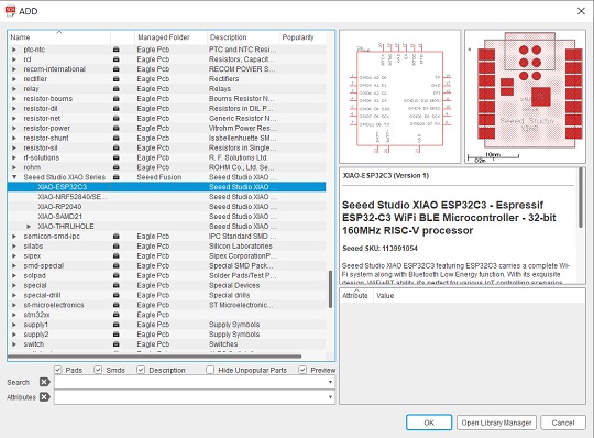
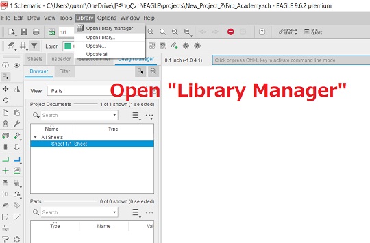
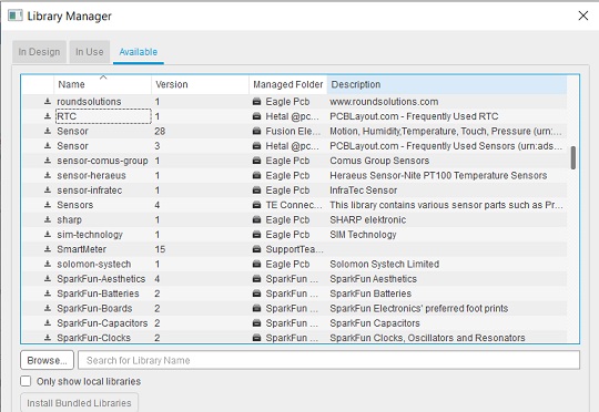
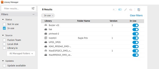
Library Manager: In case you have difficulty in finding the components you want, specific microcontrollers for example, open the Library Manager and find the library you want for downloading.
2-3. Connection: Once you place all the components, start connecting them. Clicking the “Net” icon, you could start drawing connection wires.
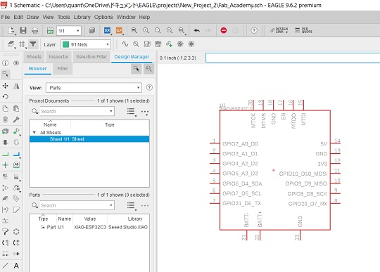
2-4. Add Values and Names: You can add specific values to the such components as resistors. By clicking the “Value” icon and then clicking the target components on the schematic sheet, you could get the dialogue window and type the value you want to attach. Similarly, if you want to assign the specific number or names to the components or connection wires, you can do it by clicking the “Name” icon and then clicking the target components or wires on the schematic sheet.
3. PCB Board Design
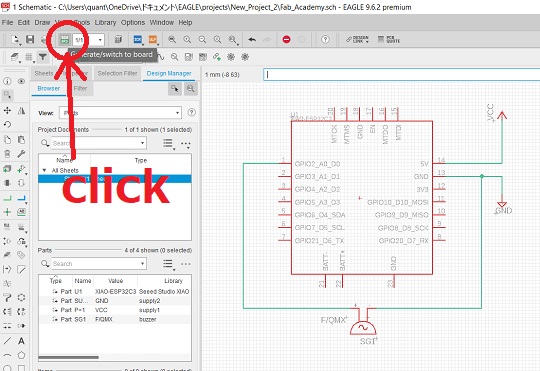
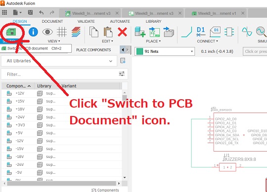
3-1. Generate/Switch to Board: You can generate the first board by clicking the “Generate/Switch to Board” icon. Then the new PCB board design window will be opened. Again, you had better save it first. You have to be careful not to close the schematic window if you want to keep the two windows in sync.
3-2. Placement of the Components: Once the PCB board design window is open, all the componentss are placed outside the board initially and you have to move and drop each one of them by ckicking the “Move” icon and dragging them one by one. After the initial placement, you have to start thinking about the best placement by moving and rotating the components.
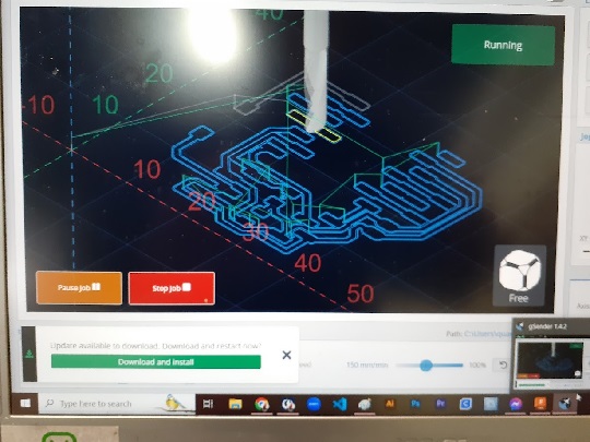
3-3. Routing: This is the process to draw wires that connect parts efficiently, and sometimes in an artistic manner. You can start drawing by clicking the “Route Airwire” icon. If you want to cancel or delete the wires, click the “Ripup” icon and pointing the mouse cursor to the lines you want to erase. In case you mill your own board by PCB milling machine, you had better draw the lines on the Layer 1, and all the wires will be colored red.
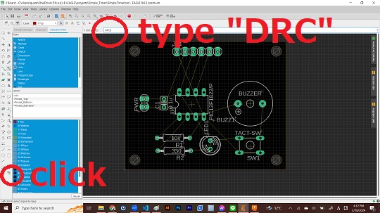
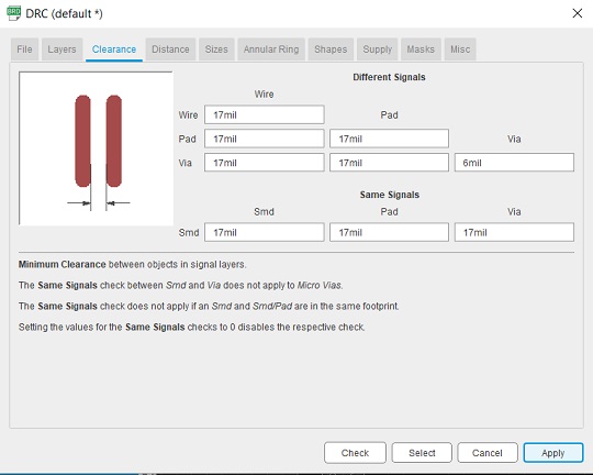
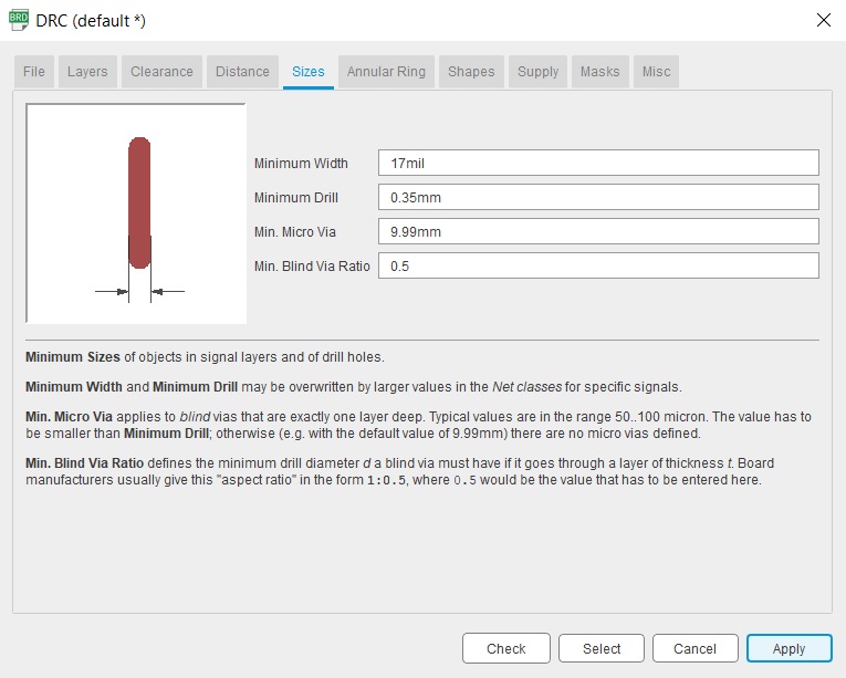
DRC (Design Rule Check): Before you enter into this routing process, you had better set the parameters about the conditions of the routes. If you use the PCB milling machine to make the board, the the diameters of the end mills are:
    Trace: 1/64 inch. (16mil) = 0.39688mm
    Outline and Holes: 1/32 inch. = 0.79375mm
To create a tool path, the clearance must be greater than the size of the end mill. Although in the DRC with EAGLE, the default clearance is set as 6 milliinches, with the PCB milling machine available in our lab, we will probably get the better results with the size a little greater than 16 milliinches for tracing. Similarly, we set the route size (width of the route) as 17 millinches as well. After changing the parameters, you click “Apply” button. You can get the DRC dialogue window eithery by clicking the DRC icon or typing “DRC” in the control panel. After clicking “Apply” button, you click “Cencel” button and then you are ready for routing. The routes will be thicker than the default setting.
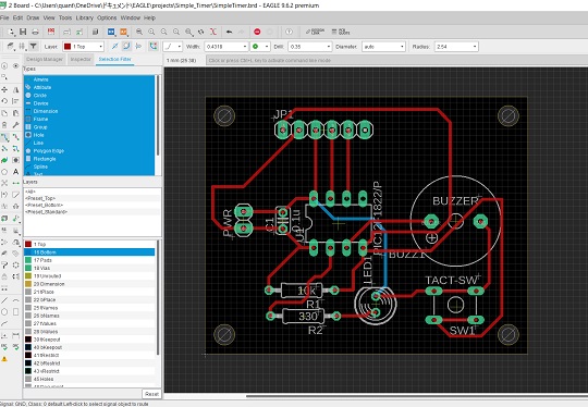
After the routing, the board will look like this. I found that the most difficult part for this exercise was if we only use the top layer for designing the schematic, we may sometimes face the situation where there is no way out. It’s almost a puzzle. If you can use the bottom or any other layer for placing addtional routes, you will have more flexibility.
After connecting all the components with wires, you had better to the DRC checking once again so that there would not be any problem in your routing.
3-4. Polygon: In PCB, if we add a copper pour to the design, it will help getting better ground signal. We fill out the open areas with copper ground patterns. The tutorial on EAGLE always refers to this step, and the procedures are well explained: Click the “Polygon” icon and set up the polygon pour conditions. After drawing an outline that covers the PCB board, you will get the “Signal Name” dialogue window and then you type “GND”. Then you could convert the solid outline to a broken line. Then the last step is to click the “Ratsnest” icon. You will get the polygon pour areas. This process could be done for the Top and Bottom Layers.
However, when we use the single-sided copper foil board (FR1) for PCB with a milling machine, the top surface is already covered with copper and there is no need for polygon pour.
EDA Design with Fusion Electronics
EDA design with Fusion Electronics was almost similar to the one described above for EAGLE.
1. PCB Design for Final Project
Since I was still a newbie in PCB design at this point of time, the ideas that could be reflected on my first EDA was very very simple.
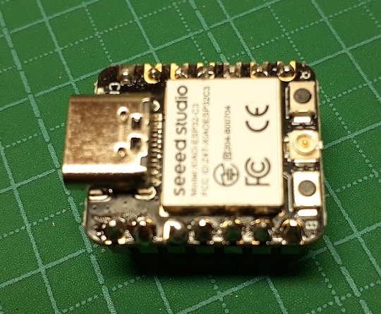
  - Microcontroller: Seeed Xiao ESP32C2
  - Buzzer: Piezoelectric Buzzer 9.8mm x 9.8mm
  - Power Supply: Rechargeable 3V Battery
Because the anti-theft alarm has to be as small and thin as possible, and it is used only for a bilateral communication within just 5 to 10 meter, I have decided to use Xiao ESP32C2, which has Bluetooth LE subsystem. It is ultra low power. It has a battery charging chip and is ideal for a variety of wearable scenarios and wireless IoT applications.
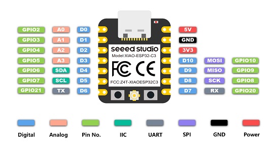
 SCL: Serial Clock Line for I2C
 SDA: Serial Data Line for I2C
 TX: TX pin for sending out (transmitting) the digital signal
 RX: RX pin for listening (receiving) for the digital signal
For the first prototyping with an EDA tool, I decided to use a 9.8mm x 9.8mm piezo buzzer. However, I am thinking of replacing it with another buzzer which could sound a siren to scare the theif. Also, while I was doing some desk research on my final project and studying ESP32 with BLE, I have started thinking of adding an LED module to the first prototype. (This was also advised by the instructors during the Asian Regional Review for Week 8.) For power supply, I am thinking of using a rechargeable coin battery for now.
2. Schematics Design
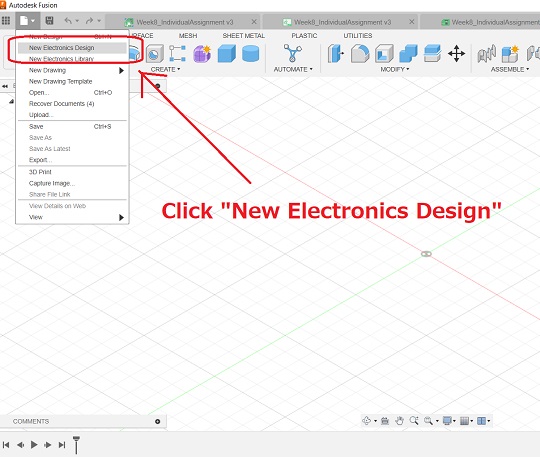
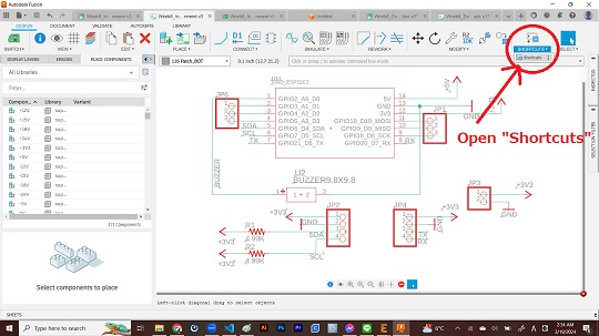
First we launched Fusion360. We could enter Fusion Electronics by clicking: “File” > “New Electronics Design”. Once we open the new project, we first save the file and created a new project. Then we click the “New Schematic” icon and open a new schematic window.
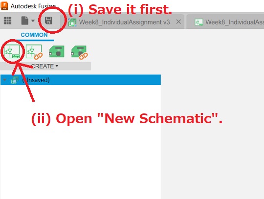
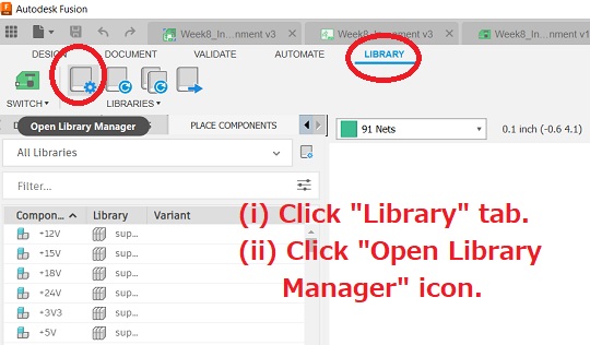
Once we open the new schematic, we had better save it first. Then we open the Library Manager and import all the libraries needed for my PCB design. In my case, I imported Xiao ESP32C2 from the Seeed Xiao Library.
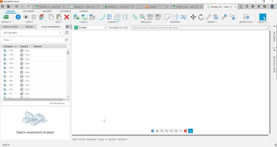
Now we are ready for placing all the components required for the schematic design. For adding components, we first type “add” and call the “Add” dialogue window.
After placing all the components, I came up with the following schematic. However, I must confess that this was made possible with the guidance from our instructor and it would take a while for my to fully understand what I did. *To be added later.
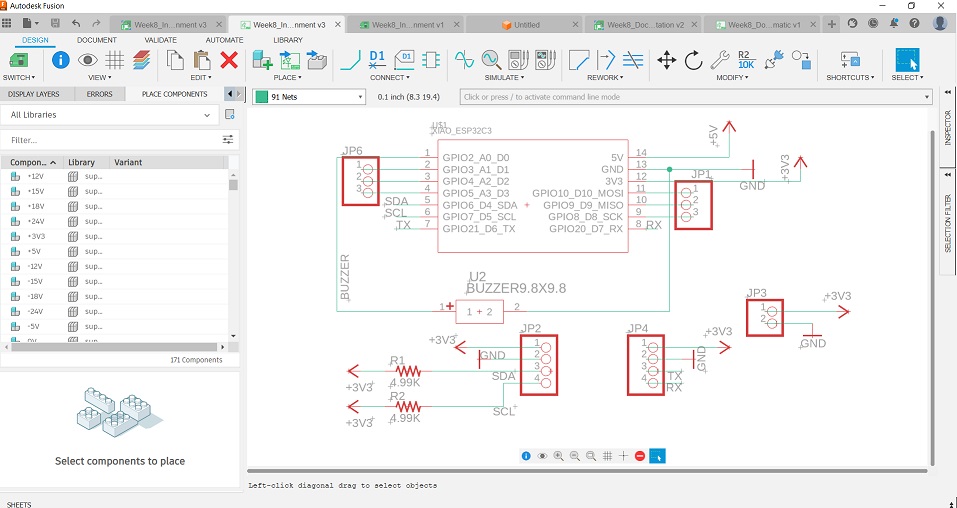
I2C:I2C is a synchronous, multi-master/multi-slave (controller/target), single-ended, serial communication bus. It is widely used for attaching lower-speed peripheral ICs to processors and microcontrollers in short-distance, intra-board communication. A particular strength of I2C is the capability of a microcontroller to control a network of device chips with just two general-purpose I/O pins and software. Many other bus technologies used in similar applications, such as Serial Peripheral Interface Bus (SPI), require more pins and signals to connect multiple devices. I2C uses only two bidirectional open-collector or open-drain lines: serial data line (SDA) and serial clock line (SCL), pulled up with resistors. Typical voltages used are +5 V or +3.3 V, although systems with other voltages are permitted. (Excerpt from Wikipedia)
3. PCB Board Design
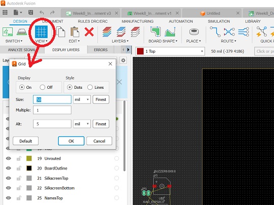
Once we get the schematics done, we click the “Switch to PCB Document” icon and open the PCB board design window. It almost looks the same as EAGLE. After switching to PCB board design, the first step to take is changing the grid setting. We click the “Grid” icon and open the dialogue window. We should make the grid visible with 50 milliinch meshes.
After placing the components, we work on routing. We have to make sure that we go through the DRC checking. Similarly to the case of EAGLE, we could call the DRC dialogue window either by typing “DRC” in the keyword search window, or by clickng the “Rule DRC/ERC” tab and then “DRC” icon. The DRC dialogue window looks almost the same as EAGLE.
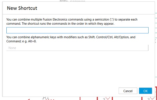
Drilling Holes: Our instructor advised on how to create holes efficiently. First we click the “Shortcuts” icon and call the “Shortcuts” dialogue window. Then we click “New” button and assign the new command to one of the function keys. In our case, we assigned the following command to F12. We have to make sure that for drilling holes we assign the Layer 116 “CenterDrill”.
SET FILL_LAYER 116 1;run drill-aid 0
For the detailed explanation of this command, we could refer to the FabLab Kannai webpage. We can drill holes by pointing the mouse curser to the target circle and pressing the key we have assigned to drilling holes, “F12” in our case.
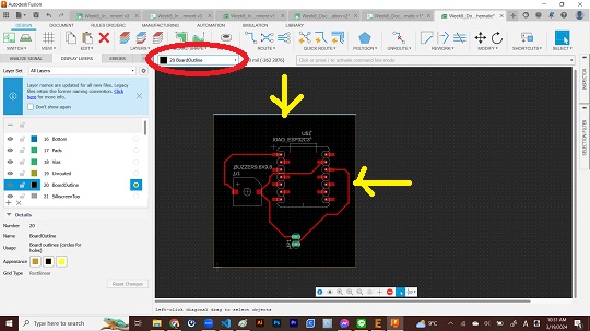
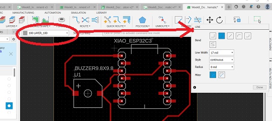
Drawing Outline of the Board: Next we have to define the outline for cutting the board. For this, we first switch to Layer 20 “Board Outline” and drag the yellow outline near to the PCB board design. This could be used as the copper board area for work.
Then we create a new layer for outline sketching. Layer 100 is automatically assigned for drawing outline.
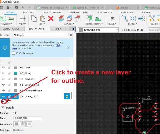
Once the Layer 100 is created, we switch to Layer 100 and type “line” to call the “Polygon Shape” drawing command.
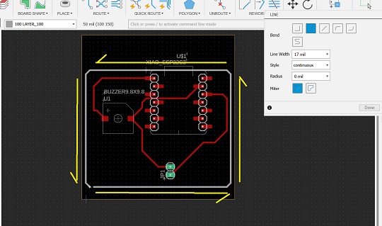
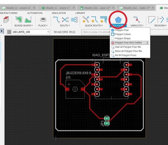
Then we draw straight line to draw a polygon. Once we make a closed area, we click: “Polygon” > “Polygon Pour from Outline”. Click somewhere on the straight line and then the layer dialogue window will be popped up. Once we select Layer 100, then the whole closed area will turn gray and the polygon pour is complete.
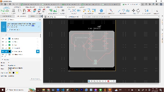
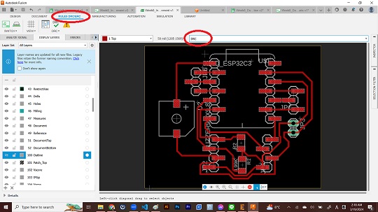
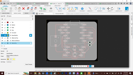
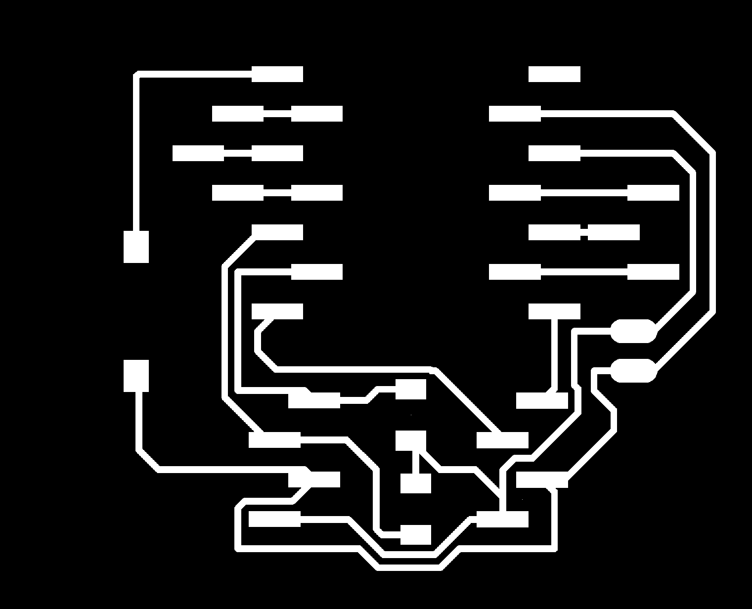
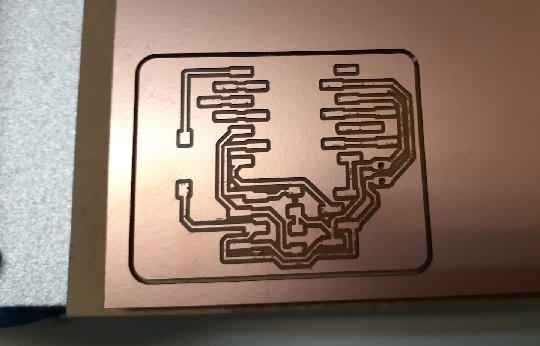
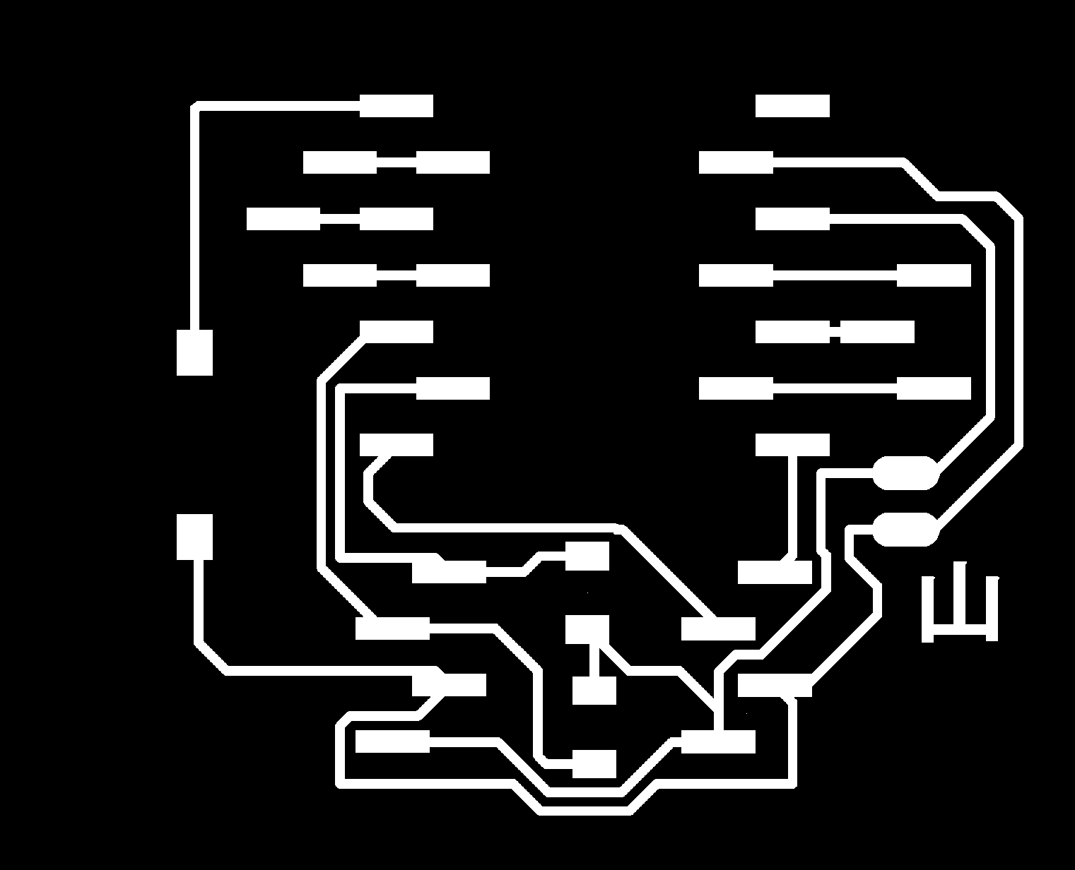
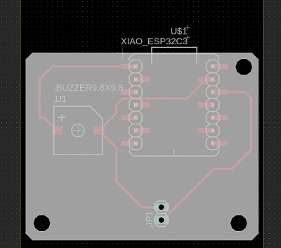
Now the first PCB board design for my final project looks like this.
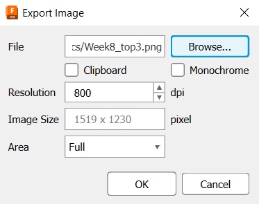
4. Data Export for Milling
Now that we prepare the PCB board design, we proceed to the data export. We once hide all layers, and then select the layers we want for exporting data in terms of PNG files for trace and outline and holes. We prepare the local folder to save the data. To call the export command, we type “export” and enter. After selecting the “Image” option in the pulldown, we can get the “Export Image” dialogue window. We set the location of the local folder and the file name. We have to be sure to check “Monochrome”.
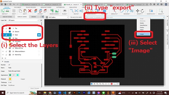
Trace: Unhide Layer 1 (Top) and 17 (Pads)
Outline and Holes: Unhide Layer 100 (Outline) and 116 (CenterDrill)

PNG Data: Trace / Outline and Holes
Milling, Soldering and Continuity Check
I followed the same process already docummented in the Individual Assignment for Week 4.
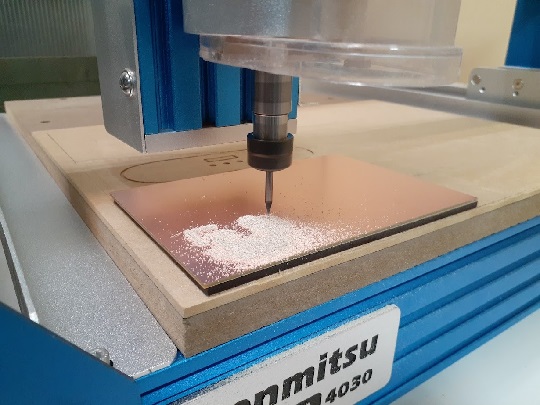
After milling out the PCB board, we mount all the components by soldering.
Although the use of the test equipment in our lab to observe the operation of a microcontroller circuit board is part of the Group Assignment, I ran out of time to use a multimeter and an oscilloscope equipped in the lab. Since the test equipment is one of the necessities in our work at home, I went to the nearest hardware shop and purchased a digital multimeter. There were many varieties of multimeters with the price range from USD 13 to 30. Oscilloscopes are not available in the local hardware shops.
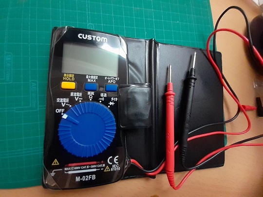
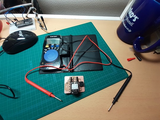
I tested every section of the circuit and confirmed that there was continuous current. However, if there was a 4.99K resistor in between, that section was silent. According to the operations manual, the multimeter could detect the current if the resistance is less than 50 ohm. Since I used 4.99K resistors, there was no current. Instead, I checked the resistance by placing two probes to each side and found that the resistance was almost 4.99K but it fluctuates around it.
Hero Shots
I hereby post a hero shot of my board. Honestly speaking, this is the second board together with the box mount I designed and 3D-printed. I documented what happend to my first board in Week9 Output Devices - Board Preparation.
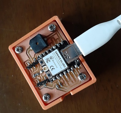
To test my board, I prepared the following simple code from the sample sketch avaiable in the Arduino IDE and uploaded it.
const int speakerPin = D0; // the number of the speaker pin

void setup() {
  pinMode(speakerPin, OUTPUT);
  }

void loop() {
  tone(speakerPin, 1000); // When the button is not pressed, keep speaker on with 1000Hz
}
Activities for Extra Credits
1. More Personalized Board
When I reached here, I remembered that there was an individual assignment which I left undone during the Week 4 “Electronics Production”. That is about personalizing the Quentorres board by replacing the “QT” logo with something else. I have decided to do it this week before I place an order to the board house.
I searched for the measures to add text or monochrome image to the board on the EDA but could not find it. Instead I imported the PNG file to the Adobe Photoshop and added my initial to the board design.
This could be fine as long as I mill the PCB board by myself. However, I have found that it was not enough in order to reflect the image in the Gerber Data. Unfortunately I couldn’t find the way to integrate the revised PNG file to the Gerber Data. Instead, in consultation with our instructor, I have found this as an altenative approach to do this:
-
First, prepare the bitmap data (BMP) of the logo we want to place on the board. Using the 2D design program, design the logo as close as possible to the real size for the board;
-
Second, in the Fusion Electronics, go to: “Automation” tab > “Run ULP” > Get the ULP on Bitmap.
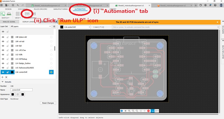
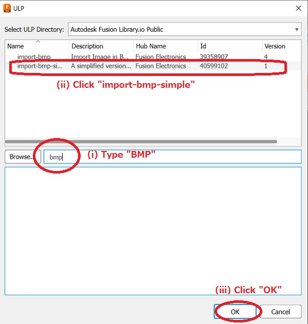
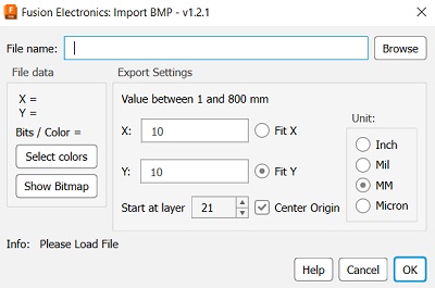
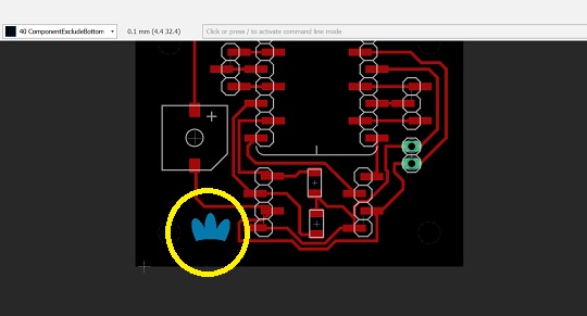
- Then, browse the BMP file and do the needful. In case there is an error message saying that the BMP file has more than 256 colors, using file converter, change the image data to monochrome. In my case, I could do it with the Paint tool of the Windows Accessories. We need much time for trials and errors to resize the image data. Once I completed the resizing, the new layer 21 “Silkscreen Top” was created for printing. I could move the whole bitmap image to the place I wanted for printing.
2. Design a Case
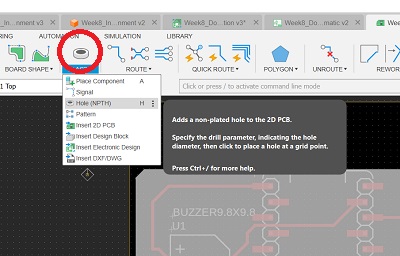
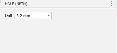
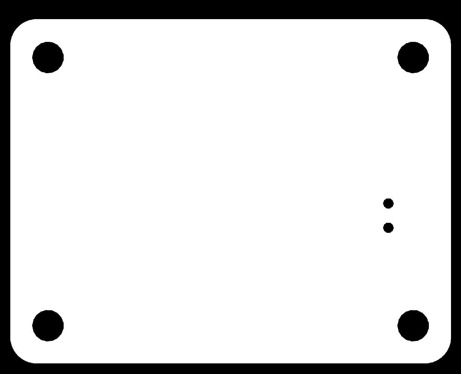
It takes a while to design and make the case to mount the board. As the first step to do it, I have added a 3.2mm hole to each of the corner of the board before I place an order to the board house. To do this with Fusion Electronics, I took the following process:
- First, click the “Hole” icon and get the “Hole” dialogue window to be popped up. Then type “3.2mm” and enter. However, if the unit is still “mil”, not “mm”, then we have to go back to the “Grid Settings” icon and change the settings from mil to 1 mm. Next time we open the “Hole” dialogue, the unit is changed to “mm”.
- Once we get the “Hole” image on the workplane, move the Hole image to the place we want to create the hole and click. Repeat this operations until we complete placing all the holes. We can stop the placement by clicking the “OK” button in the “Hole” dialogue.
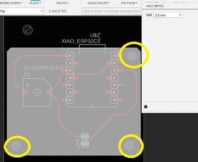
- Then we pressed F12 to drill holes on the hole images. (F12 is defined by the users. )
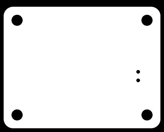
- Finally, we leave the outline and holes unhide and export the image file in terms of PNG file. *To be added later.
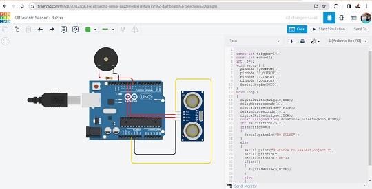
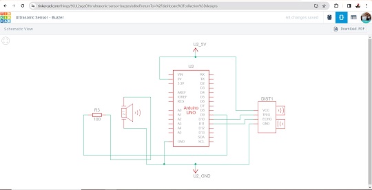
3. Try Another Design Workflow
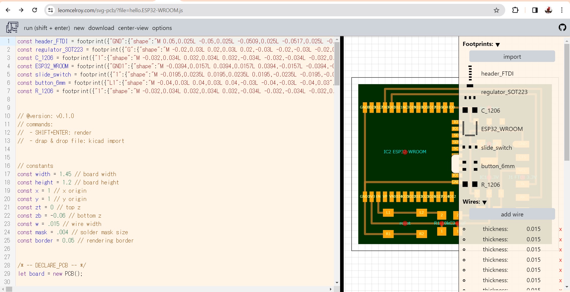
Tinkercad: First, I experienced Tinkercad as it also had the electronic circuit design feature. However, I found that it’s good for EDA with micro:bit and Arduino. But it didn’t have Xiao microcotrollers variety and they don’t have libraries. We could design the circuit and schematic. But we were not able to proceed to PCB design on Tinkercad alone.
SVG-PCB: I also experienced SVG-PCB, which was a browser-based editor for designing PCB boards by writing codes. *To be added later.