4. Electronics Production
Weekly Highlight (February 15 to 21)
-
Spent much time repairing the 3D printer (Creality CR-10S) at office, JICA Research Institute. It was nozzle stuffing and I fixed it by replacing the nozzle.
-
Spent much time reading the characteristics of the PCB milling machine of FabLab Kannai, Genmitsu PROVerXL 4030.
-
Had hard time in soldering SMD devices on the circuit board because of my eye problem. But some past experience with Arduino IDE helped me to catch up.
-
Glad to hear that my home lab, FabLab CST Phuentsholing, sent many participants to the makeathon for designing assistive devices for the Special Education Needs (SEN) children, organized in Thimphu, Bhutan, on February 15-17, and made great contributions. For details, please read the article on Kuensel, national news daily.

Photos courtesy to FabLab CST and Naoki Hamanaka
Assignments Overview
Here is the list of individual assignments given by the instructors. As for the Group Assignment, please see the Group Assignment page on the FabLab Kannai website:
- Make and test a microcontroller development board
 [Extra credit] Personalize the board
 [Extra credit] Make it with another process
PCB (Printed Circuit Board) Fabrication
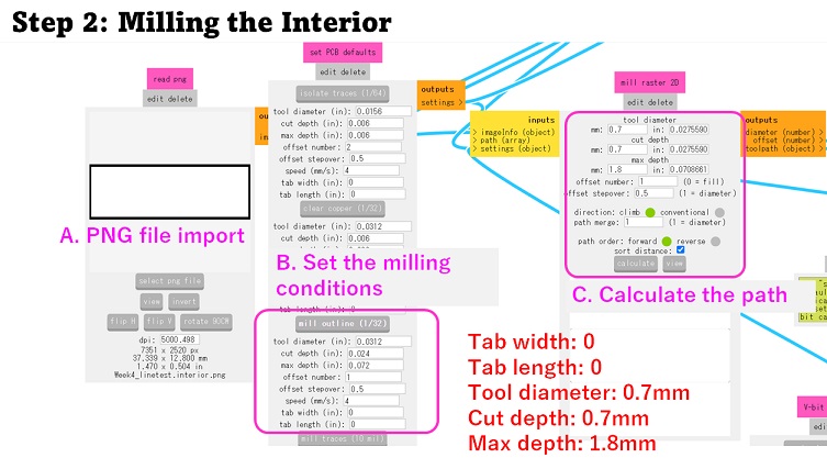
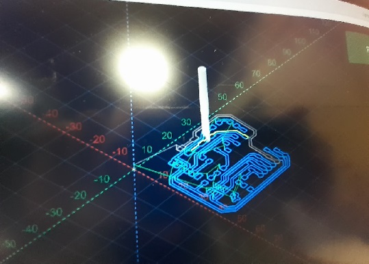
The process to cut the PCB board for making a microcontroller development board in the individual assignment was almost the same as the one to cut the sample measure to check the cut results with our PCB milling machine: Genmitsu PROVerXL 4030.
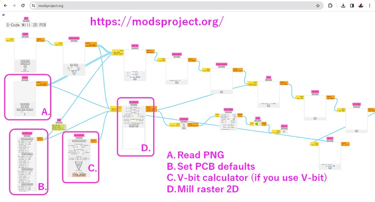
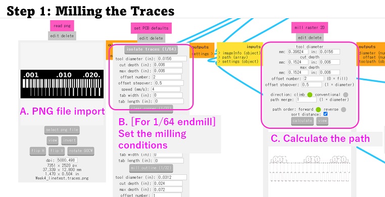
Two sample data were provided in terms of PNG file: Traces / Interior
For milling the trace and interior, we used the different bits. Everytime we shifted from the trace to the interior or vice versa, we should be mindful enought to change bits.
| Target | Bit Choice | |
|---|---|---|
| 1 | Trace | 1/64 flat endmill (=0.4mm) |
| 2 | Interior | 1/32 flat endmill (=0.8mm) or 0.7mm endmill |
| I didn’t try 30 degree V-bit for milling the trace. Ito-san chose to remain with V-bit. |
Here is the video of the PCB milling operations we made on Saturday, February 17, 2024, at FabLab Kannai.|
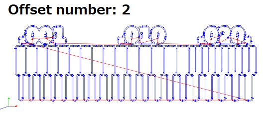
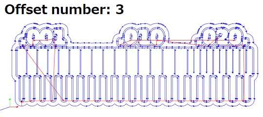
The following two images are for the comparison of the expected outcome and the final result.

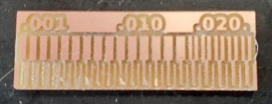
PNG file shows that the width of the white band gradually increases from 0.01 to 0.20 inches by every 0.01 inch and the copper sheet is peeled off at 0.13 inches. Also, it fails to mill the black band if the width was less than 0.15 inches.
How come couldn’t we get the expected outcome? I reopened the mods CE gcode generator and had it read the PNG file. Then I changed the cut width, max width and offset number on the PCB default setting window and saw the results.
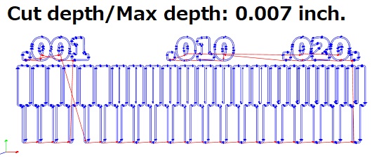
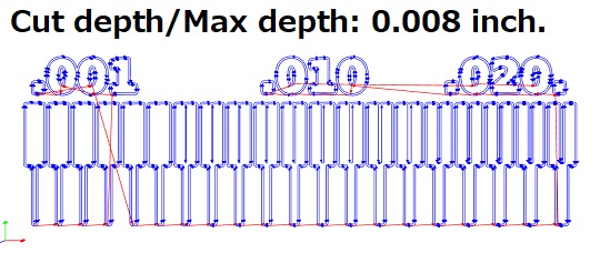
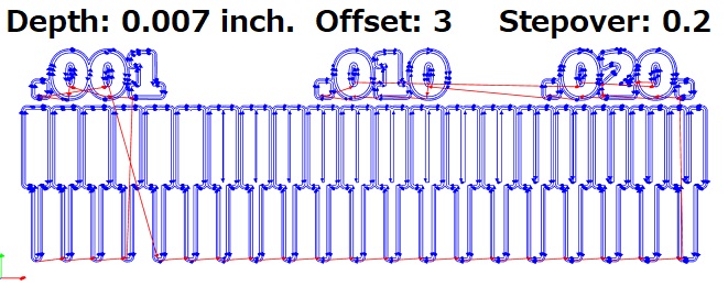
My tentative conclusion is that if I want to have a clear black band with the width as less than 0.15, I had better increase the cut depth and max depth beyond the default (0.006 inches). Our instructors have advised me that the depth should be a half of the diameter of the endmill (between 0.007 and 0.008 inches).
As of February 21, 2024, I have not found the best parameter sets to surely have the black band until 0.01 inch. But our instructors have indicated us about the following two possibilities:
-
Spindle RPM: If it’s too fast, it may affect the result.
-
Conditions of the Endmill: Endmill is expensive but perishable. The damage on the endmill may affect the result. Especially it may affect the offset milling range. We also have to be mindful of plunge rate (speed to plunge the endmill vertically). If it plunges too fast, it may damage the endmill. Lastly, we have to ensure that the endmill is mounted deeply enough to the collet. If it’s not deep enough, the vibration of the endmill, or runout, becomes larger no matter if we set the toolpath accurately. This will affect the milling result, too.
Making of a Microcontroller Development Board
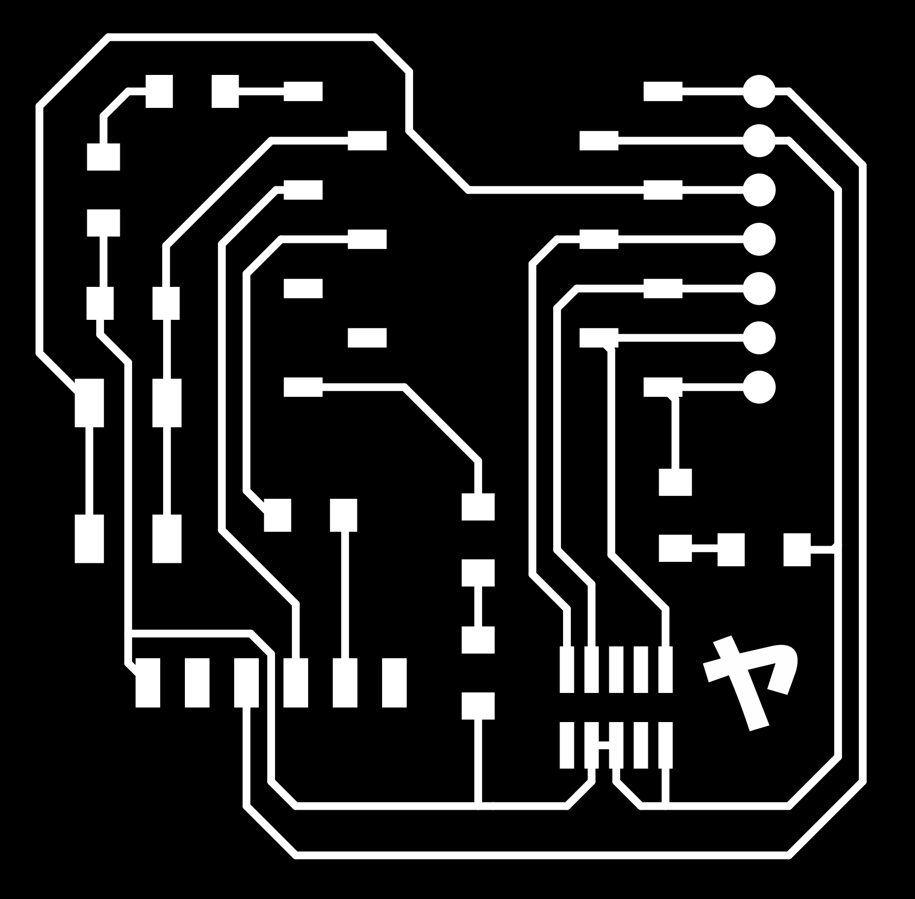
1. Board to Mill “Quentorres”: I first went to the Quentorres gitlab and downloaded the three PNG files of the board (Traces, Drill Holes and Interior).
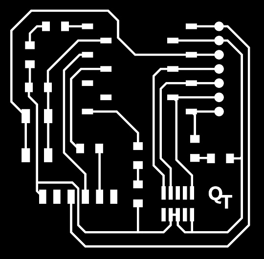


2. G-Code Generation with Mods: Then I opened the g-code generator and had it read the PNG files and generated three g-code files. Initially we had been thinking of using V-bits for milling the traces. However, the first volunteer, Itoh-san, and our instructor faced difficulties in getting a good milling result even after a series of finetuning. Therefore, Itoh-san and I decided to use the 1/64 flat endmill for the traces. For holes and the interior, we used 0.7mm flat endmill.
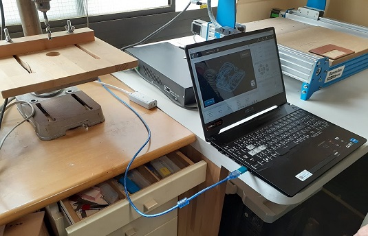
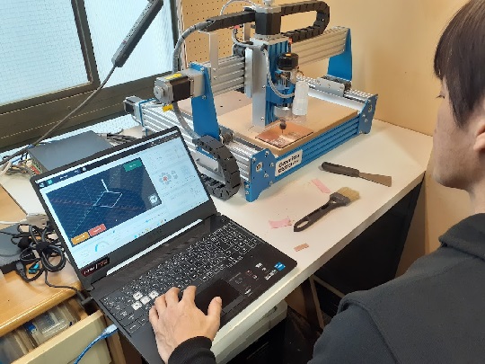
3. Downloading gSender: While we were working on the group assignment, we downloaded the gSender, CNC control platform to send the g-code to the milling machine.
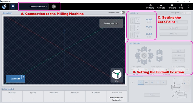
4. Switch-on the Milling Machine: After installing the gSender, we connected our laptop to the milling machine and turned on the machine. Once the gSender was activated, we set up the connection by choosing the serial port in the pull-down menu under the switch-on icon on the top left cornerof the control panel.
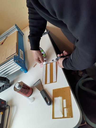
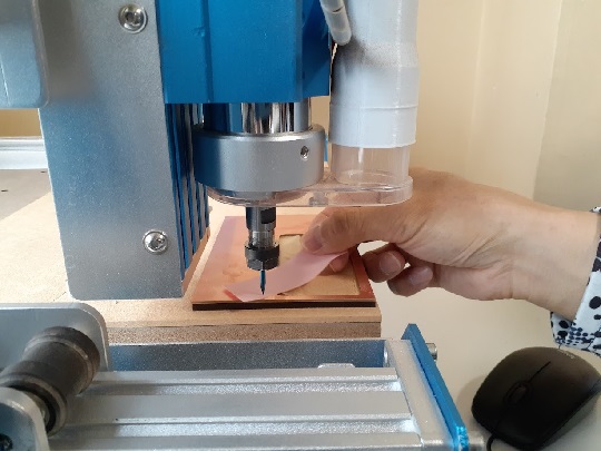
5. Installation of the Copper Board to Mill/Cut: While the endmill is standing by at the top-right corner of the board, place the material (paper phenol board or FR1, in my case) on the front left corner (origin) of the table. It would be better put a few pieces of double-sided tapes on the back side of the board and had the board and table sticked to each other.
6. Installation of the Right Endmill: Before we move the endmill to the starting point, we had better replace the endmill with a right one. You can loosen or tighten the collet.
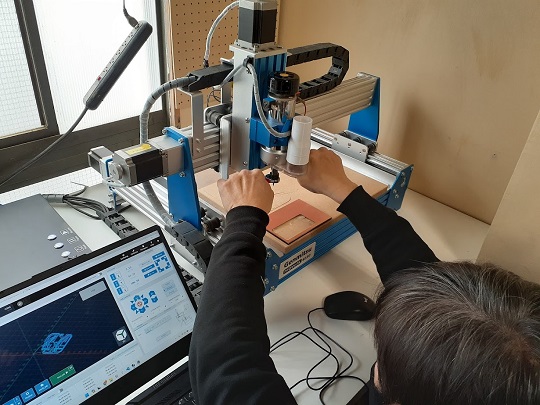
7. Jog Control: Once we installed the endmill, we move the endmill along the X and Y axes to the point it starts milling oprations. Once we set the XY origin, we reset the X and Y positions to zero on the “Location” panel. Lastly, we moved the endmill vertically along the Z-axis. You should bring it down to the point where you are not able to remove the paper. Once we set the Z origin, we reset the Z positions to zero on the “Location” panel.
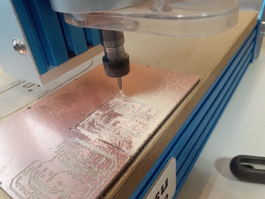
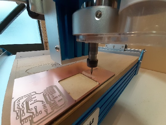
8. Start Milling: Now we could open the g-code file and start the job. Do the milling process in the order of (i) Traces > (ii) Drilling Holes > (iii) Interior. It took 20-25 minutes to complete all the three jobs.
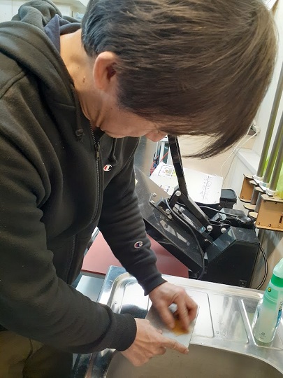
9. Clean-up: Once the board was milled, I poured solvent on the outer cut line so that I could remove the board off from the double-sided tapes. You could slide the scraper into the ditch of the cut line and pull out the board. You could also remove all the tapes sticked to the cut-out. You can now switch off the gSender by clicking the power button on the control panel. Also, be sure to clean up the environment by vacuuming the dust.
10. Deburring: We removed burr from the surface by rubbing with a sanding spong and water.
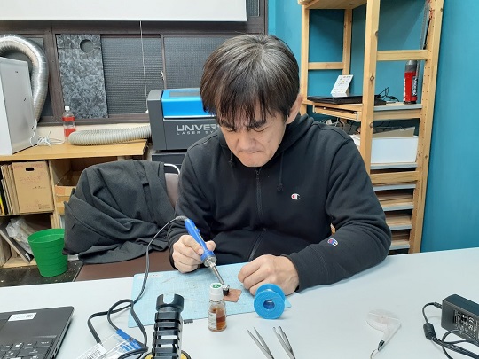
11. Soldering!!!: This is the most difficult part of the assignment for this week for me. After checking the items and numbers required for assembly, we started soldering works, starting with the two headers with seven legs to the board, on which we could connect XIAO RP2040. Then after that, we were advised to solder with the devices with low height and placed near the center of the board. That would help us to finish soldering easy and quick. However, my presbyopia in my left and astigmatism in my right eye made it extremely difficult for me to place soldering iron head and the tip of the wire in the target pad. Sometimes my soldering work was not enough to ensure good connection, and sometimes I formed a “bridge” between the two soldering points. In the latter case, I had to remove the solder wtih the solder removal tape.
Additional Notes:
-
As for soldering, I found this book was useful. Of course I know that the reality is practice makes perfect. Marc de Vinck. 2017. Getting Started with Soldering: A Hands-On Guide to Making Electrical and Mechanical Connections
-
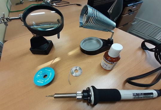
For other purposes, I have purchased the set of soldering kits for the use at home. They include: soldering iron, solder (lead-free wire), removal tape, ironing station, flux, tweezers, and magnifier. (However, after reading the above book on soldering, I came to know that one critical item was missing: Eye shield.)
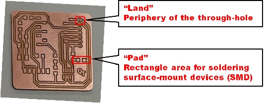
- Land vs. Pad: While reading the above book, I have frequently faced the words “land” and “pad”. Both seemed to mean a small area of the copper foil on the PCB board. After studying the terminology, I understood that “land” is used for mounting through-hole components while “pad” is used for soldering surface-mount (SMD) devices. In our assignment, we used only SMD headers, LED, chip resistors and tactile switch. Therefore, I am using “pad” in my documentation.
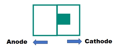
- LED Anode and Cathode: When we use SMD LEDs, unlike the through-hole LEDs, it’s hard to distinguish anode from cathode. In the case of the LEDs we used for our assignment, it was learned that the green sign on the bottom surface of the LED devices shows it’s the cathode side.
- Soldering SMD Devices with a Soldering Iron: In our assignment, we tried to solder the SMD devices with a soldering iron. Since the SMDs are too small and don’t have legs to hook on the land of the board, it’s hard to hold them in the right position connecting two pads. In this case, we had better hold them with tweezers and use pre-tinning technique, which means we put solder on one pad beforehand and place the device later for connecting. Also, we had better not forget about covering the pads with flux. That will help us to solder smoothly. However, there is an alternative method for soldering SMDs, using a reflow oven.
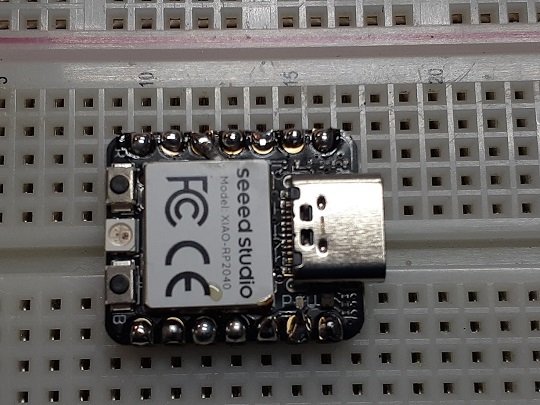
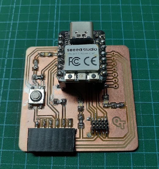
12. Checking: Now that all the soldering works were done, the microcontroller development board looks like this. Using a multimeter, I checked the electric current between sections of the circuit board. Although I had been a bit worried about my poor soldering skill, the current was detected at each of the sections.
Test Programming with Arduino IDE
Now the microcontroller board is ready. It has three LEDs and a button and is a good entry model to learn how to program with Arduino IDE.
1. Installation of Arduino IDE: I have experienced coding with Arduino IDE before. I could skip this step.
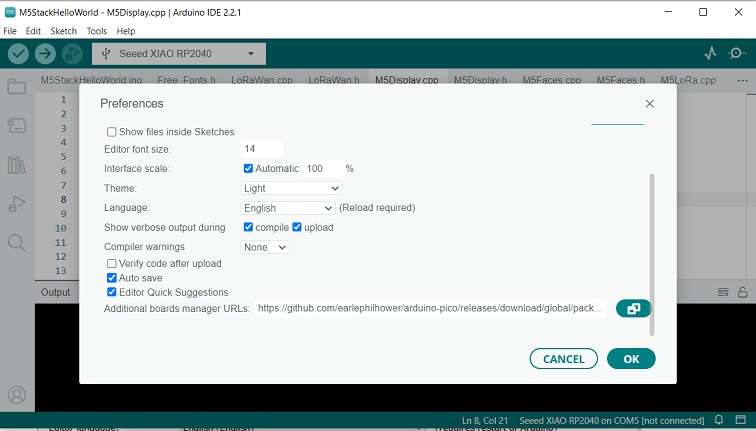
2. Additional Board Manager: Open the Ardino IDE and go to File > Preference > Setting. Then open the gitlab Arduino-Pico by Earlephilhower and copy the Additional Board Manager URL. Then go back to the Arduino IDE preference dialogue window and paste the copied URL
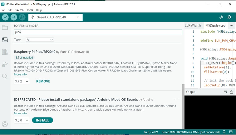
3. Downloading “Pico”: Go to Tool > Board > Board Manager, and search by typing “pico”. Once you find the “Raspberry Pi Pico/RP2040 by Earl F. Philhower III”, click “Install” for downloading.
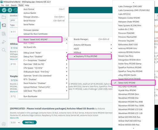
4. Configuration for XIAO RP2040: Go to Tool > Board: “Seeed XIAO RP2040” > Raspberry Pi Pico/RP2040 > Seeed XIAO RP2040. Then the Seeed Studio XIAO RP2040 appear in the serial port, in my case in COM 5.
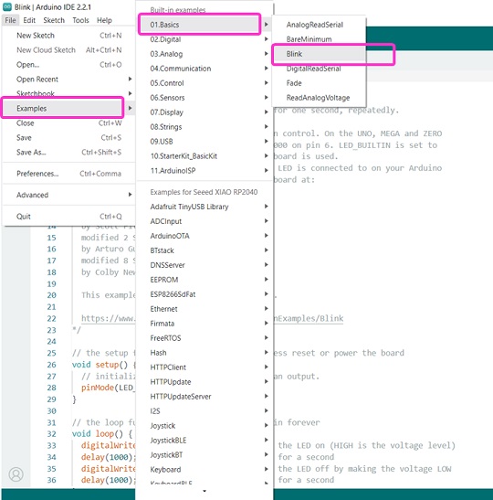
5. Load LED Blink Program from Library: Go to File > Examples > 01. Basics > Blink. Then you get the basic code for blinking LED.
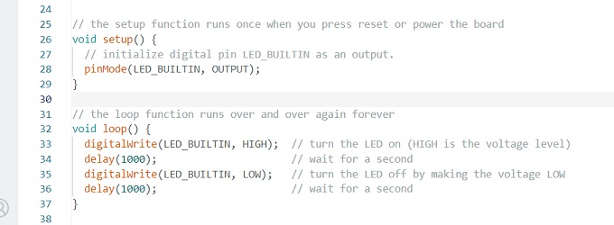
Now you have to modify the basic code by replacing:
   LED_BULLETIN to GPIO Pin number (26 / 0 / 1)
   Delay (Sleep Time): 1000 to the number you want.
Once you write codes, click “Verify” to check the code and then click “Upload” to flash it to the board. Changing the codes for GPIO and sleep time, the LEDs blink differently as described in the attached video.
Apologies for making a spelling mistake of Quentorres
Placing Order on the Board House
Placing the order for board production was part of the group assignment for extra credit. Also, personalizing the microcontroller development board was one of the individual assignments for extra credit. Since I did the first microcontroller board making with the original Quentorres logo, I have deciced to redesign the board with my personal logo and place an order on the board house in the weeks later.

Replicating the Board by Alternative Process: Reflow
I understand that for soldering surface mount devices (SMD) on the board, we often use an alternative process: reflow. Next time I have a chance to solder on the microcontroller board, I will try this technique.