Electronics design
| Task | progress |
|---|---|
| Linked to the group assignment page | done |
| Documented what you have learned in electronics design | done |
| Checked your board can be fabricated | done |
| Explained problems and how you fixed them. | done |
| Included original design files (Eagle, KiCad, etc.) | done |
| Included a ‘hero shot’ | done |
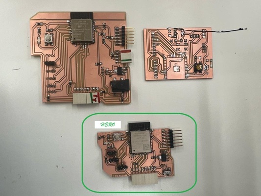
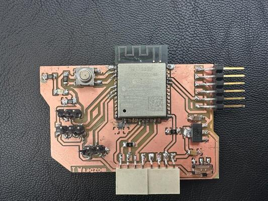
Hero Shot
Group Assignment
The link to the group Assignment is here.
Takeaways from this weeks group assignment:
- Oscilloscope is a great tool visualize your work though waveforms.
- It can be also used for checking the signal output, the voltage and change in voltage with time.
- Multimeter is a very handy tool when making your board especially to check continuity which helps debugging the circuit.
Electronics Design with KiCad
I decided to use KiCad as my design software as it is more prefered in fab community for being open source and my instructors said it is easier to use. I wanted to start making the board for my final project and started by researching about the number of pinouts I will be needing.
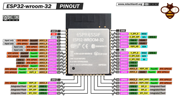
I was coming out to be more than Xiao can handdle so I decided to make use of ESP32-Wroom-32 as it had many GPIO pinouts.
I studied the datesheet of ESP32-wroom-32 and planned out the pinouts.
Here are the pinouts I researched for ESP32-Wroom-32 that I am thinking of using in this board. (Might be wrong, need to crosscheck again)
Got the image below from mischianti.org from internet.
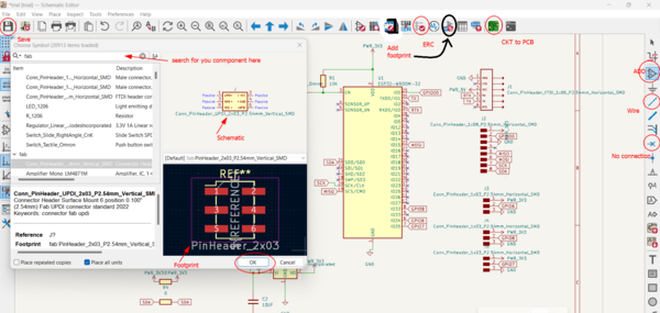
KiCad design
I followed the instruction in the KiCad tutorial by Barcelona Here to install the footprints and start using the software.
-
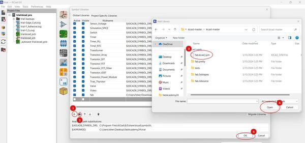
Downloaded from here the fab librabry for KiCad.
-
Install the fab library and footprints by going to preferance and Manage symbol library and adding the folder that was downloaded from the link above as shown below. For Footprints follow the same step but got to * manage footprint then select the fab pretty* folder.
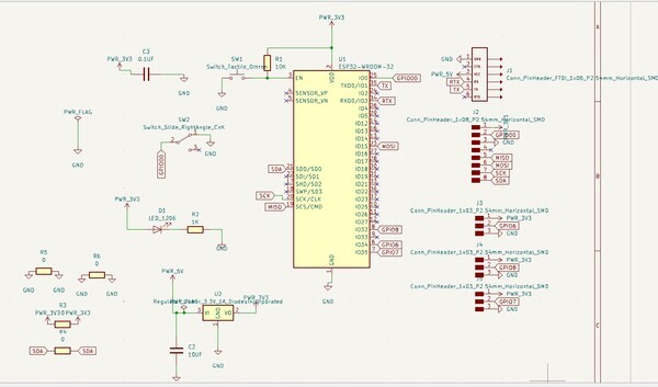
- This is the circuit I created. I used the Add feature to add the components I needed and connected using wire. Instead of drawing the circuit I decided to use the Global label to connect the components.
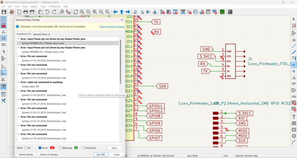
- While desinging you need to check the ERC (Electrical Rule Check) which helps you debug your circuit and also given errors in your circuit. As you can see, I got a lot of errors and warnings.
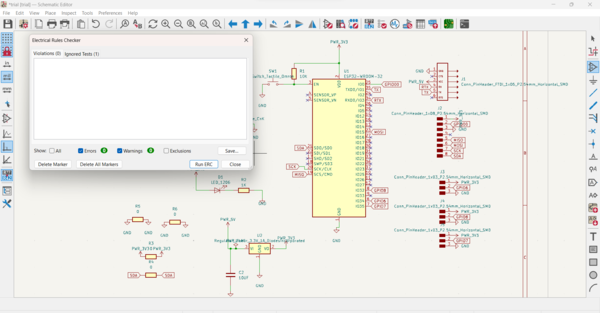
- This was after I corrected all my errors.
-
Time to make my PCB board. I created the PBC by clicking on the CKT to PCB shown above.
-
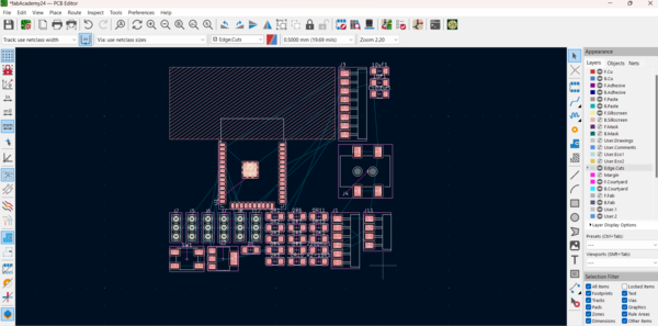
The schematic gets transferred to PCB editor and this is how it gets transfered.
Note
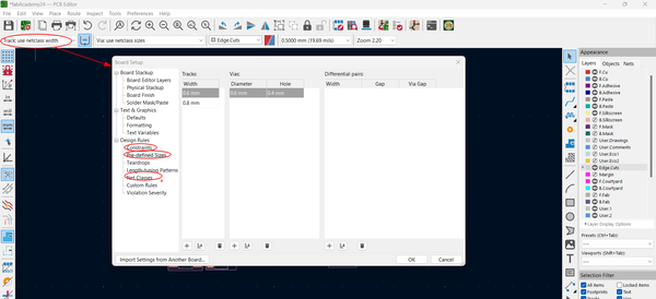
Before starting with the PCB design, design rule like setting constriants, and pre define sizes are necessary. You can find the details in the barcelona tutorials
I used Track width 0.4 and 0.6 and for power line 0.8. I gave constraint of 0.375 as this was the minimum contraint required for ESP, which showed up during DRC.
-
Next arrange the components and it is best to take time and make good decision on the placement.
-
Components can be connected/routed (Shortcut X) as placement takes place simulatenously but I prefered arranging and routing and again change the position of the components.
-
Zero resistors can be used as jumpers in those places where it is impossible to route and I used quit a few on my board.
-
Updated the board everytime I add a component in Schematic.
-
To make the border of the board, select the edge Cut layer and draw with the help of line/ shapes. In my case I used line because of its irregular shape.
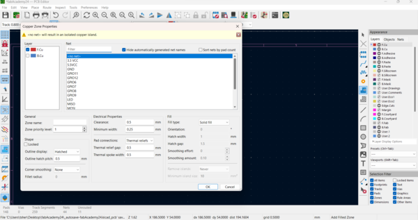
- Ground plane was made by using Add a fill zone feature and drew on the board along the shape of the board as I wanted ground plane all over the board.
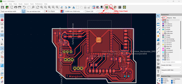
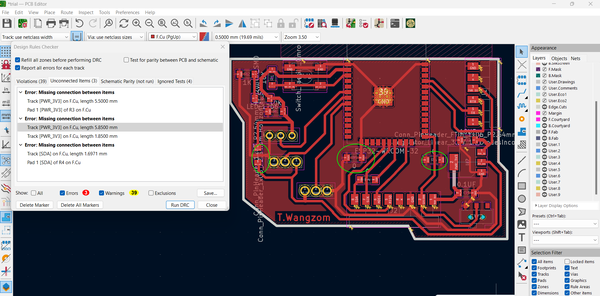
- Finally, checked if everything is right with my design by doing the DRC.
Below are the errors, I could not fix , as it was showing error for not connecting 0 Ohm resitors, which can be ingored and also other warning are for silkscreen.
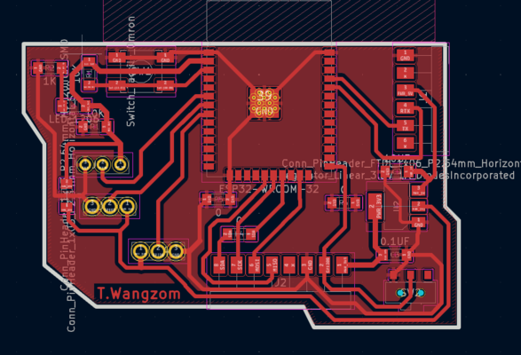
Final board.
Fabrication and testing
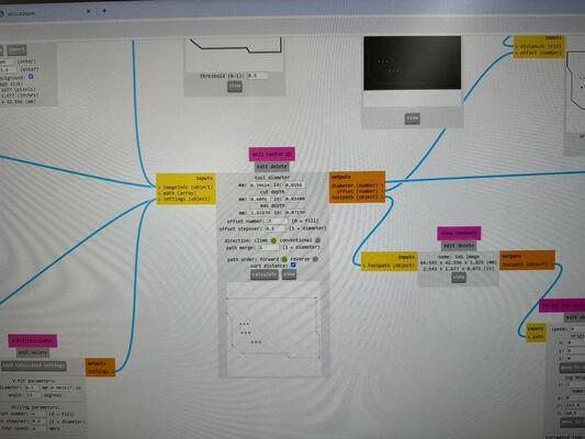
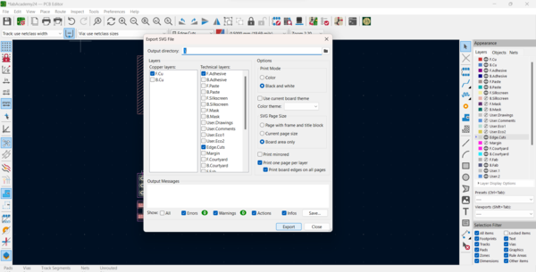
I downloaded the svg files for the board from the kiCad by going to File–> export–> .SVG
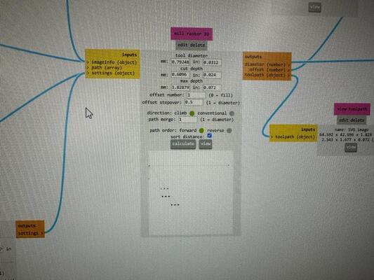
- Took the boards SVG file to Mods and then milled using Roland SRM using 1/64 bit. You need to invert the SVG file in MODs to get the right rml file.
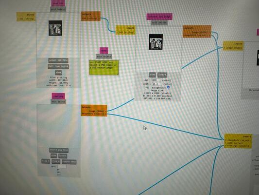
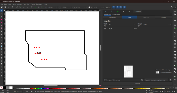
- For the border and drill files, I opened the board SVG in INKSCAPE and deleted everthing other than the drill and boarder. Saved this as a new SVG file for MODs which will be milled using 1/32 bit.
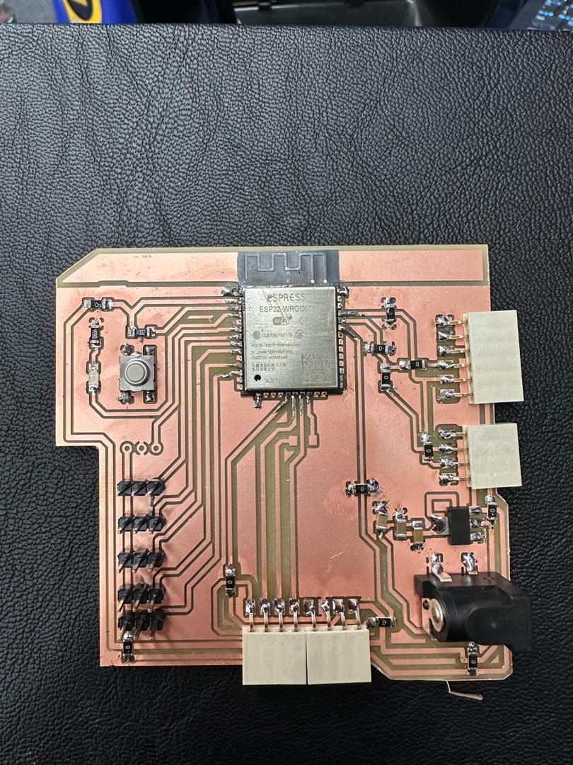
Time to Solder the Board
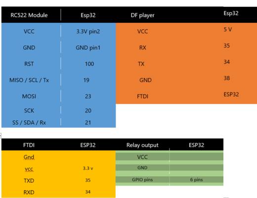
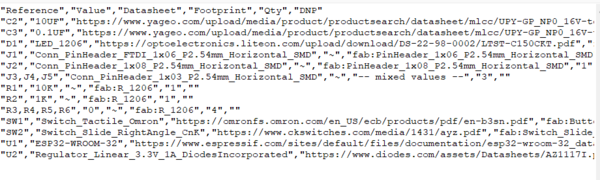
Here are the components I used in the board.
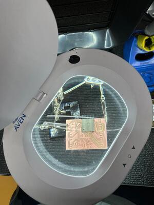
Soldering ESP was challenging and took the most time. It was best to do it under a magnifier and checking continuity between the ESP leg and the PAD after soldering.
Here is my board that actually worked. I did blink test and it was working.
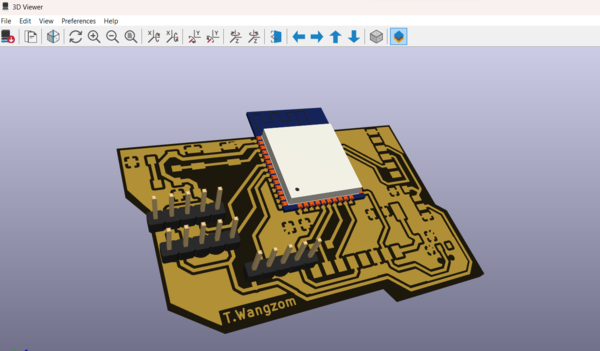
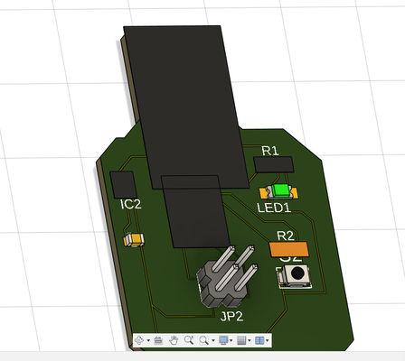
This is how it looked like in 3d view.
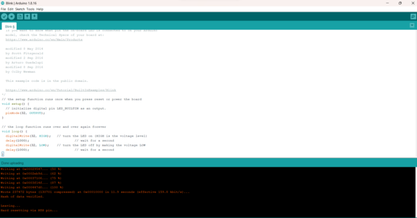
To load the program in ESP-Wroom_32, you need to turn on the Reset button connected to GPIO00 while uploading, and when done uploading, slide the switch to gnd and then press the Enable button.
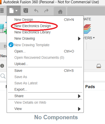
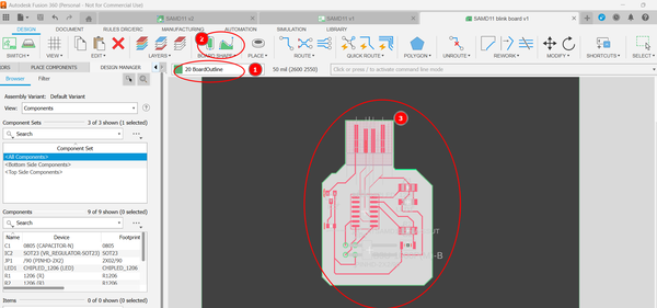
Electronics Design with Fusion 360
I also wanted to try using Fusion 360 as it was new to me and I previously used Eagle for PCB design. Wanted to try the 3d view of the ckt. I didn’t do ERC or DRC here as I just wanted to get the feel of the software. I would say, KiCad was comfortable to use as I got used to it.
- So for Fusion360 we can create a new Electronics Design, create New Schematic.
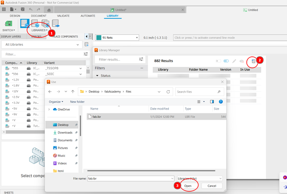
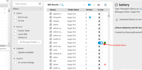
I also downloaded the fab library for the fusion360 from here. Also we need to enable the library for those library we want to use. It is better to do this otherwise lot of library gets loaded.
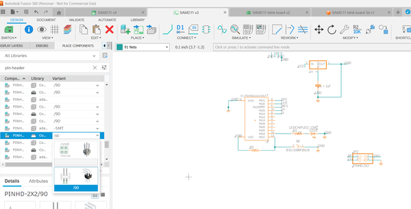
- It was nice to be able to see the 3d view of each component beacuse then I was sure which component i was using. It has very good build in Library.
Finally I used Auto-route to make the PCB and drew the board outline as shown below.
Failures and Learnings
For this week I had lots of learnings from my failures, I made three boards in total and I had a tought time debugging them.
Board 1
For this board, I was too ambitious and was trying to make my final board. In the process I forgot to add reset button and also from FTDI cable I forgot put in a voltage regulator as I was thinking of using power from jack.
-
Using a jumper wire I could solve the power problem by removing the power from FTDI cable but because I did not have a reset button, I was not able to program the board.
-
Also somehow I forgot to route the button to enable pin, which i used jumper wire to program.
But my power source from Power jack worked.
Board 2
-
In this board I used Tactile switch instead of slide switch which was my first mistake.
-
Secondly, I had not routed the 5 VCC from FTDI cable in my schematic but 3.3 volts but I used the jumper wire to give the power supply to the regulator to test but it was still not working.
-
There was Power Surge Error on my Laptop when connecting FTDI cable. I Realized this was because I had accidently connected 5v and 3.3v in regulator, while soldering, which was demanding more that 5 volts from USB port.
MODs Issue
When milling the first board, there was problem with traces with svg file downloaded using plot in kicad and same was for png images. The rml file was not milling the ESp32 pins connectors. SVG file exported from KiCad was the only file working.
For the third board I faced problem while milling the board. Somehow MODS was NOT detecting the edge when using 1/32 bit.
What I did to solve this problem was in 1/64 bit setting I gave 1/32 bits setting but didn’t change the bit size and that successfully milled the board.