Electronics Design
Group assignment:
- Use the test equipment in your lab to observe the operation of a microcontroller circuit board (as a minimum, you should demonstrate the use of a multimeter and oscilloscope)
- Document your work on the group work page and reflect on what you learned on your individual page
Individual assignment:
- Design a development board to interact and communicate with an embedded microcontroller
Analyze the MCU
As I'm following the Fab Academy remotely, I'll test my equipment here. Unfortunately, our lab is not that well equipped with electronic test tools. We only have a multimeter. But a friend of mine loaned me a USB meter (to measure power consumption used for lithium batteries) and a Hantek 2d72 a simple handheld oscilloscope (2CH, DMM, AWG, 70Mhz).
Power consumption
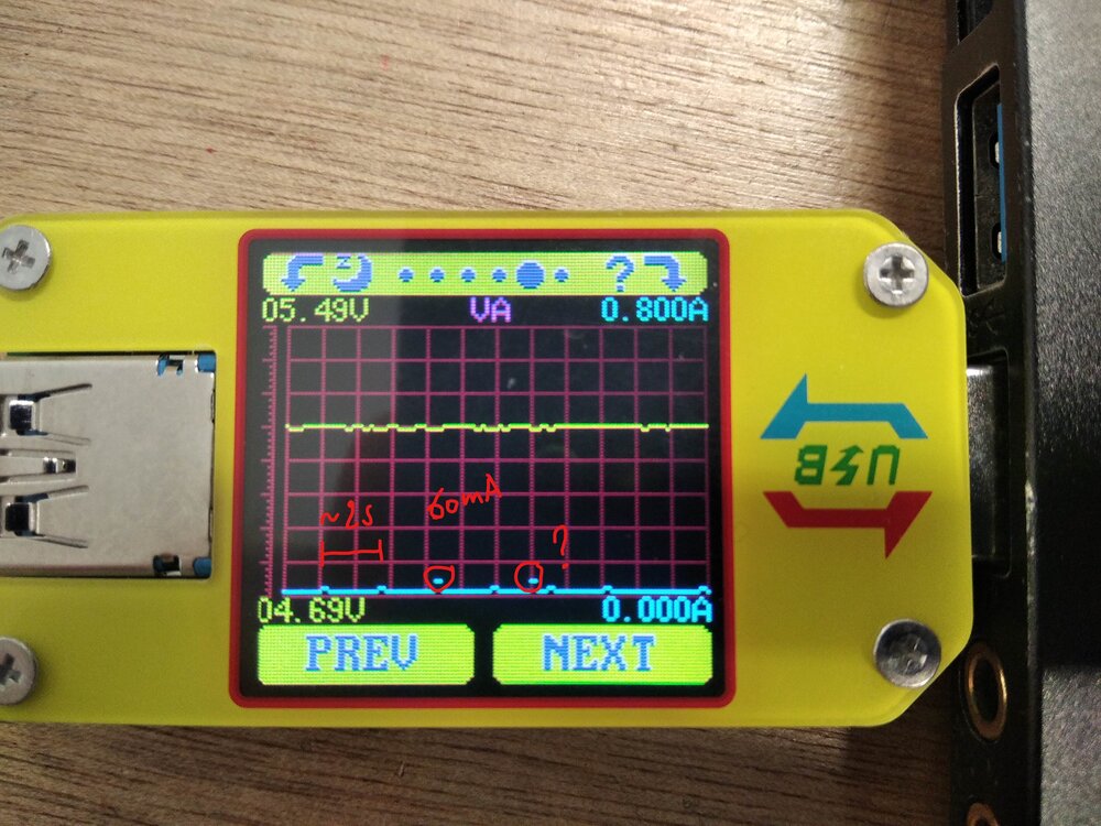
First I measure the XIAO ESP32C3 with the DHT11 sensor I built in Week 4. All I need to do is to plug the board into the USB meter and look at the result. The result shows a current that varies a lot.
Most of the time the value is around , but sometimes it's jumping to or even . In the original code, I was retrieving the Sendor value every . In the USB meter graph, it seems around every 2 sec, precisely. But sometimes there are other peaks. For that, I guess it's the WIFI and the webserver. I've added the Wifi connection and a web server in the code. So probably I consume more because of that.
So I decided to connect a brand new XIAO ESP32C3 to see the difference. Actually to consume more and consistently (~around ).

I did it for the SAMD21 connected to the RGB LED and the Joystick and also for the RP2040.
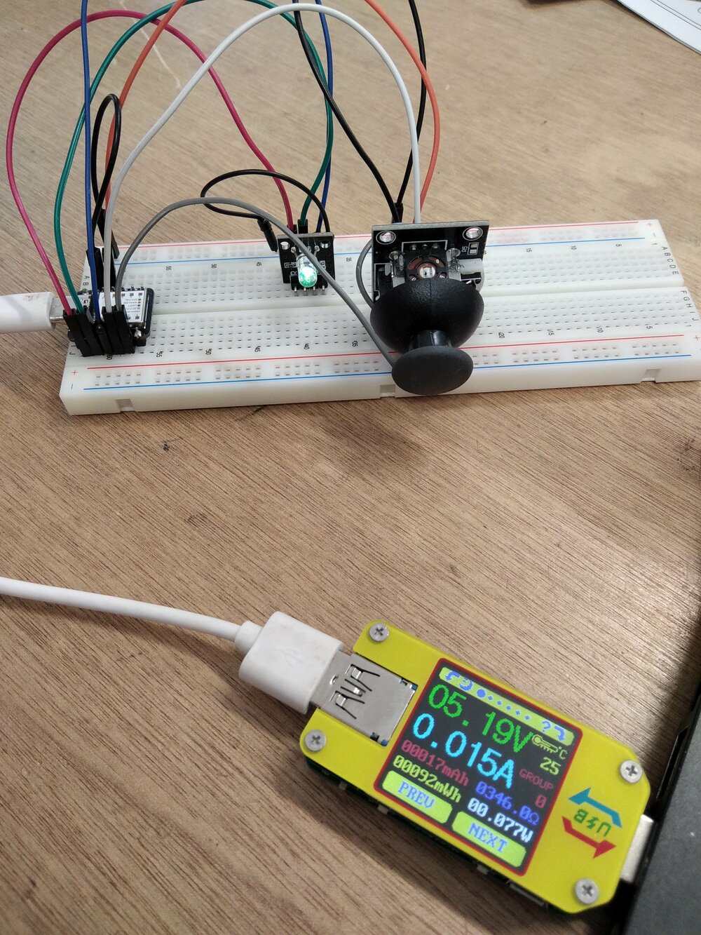
Apart from the current, the voltage is pretty constant around 5,18-5,19V for tall the boards.
Here are all the results:
| XIAO Board | Voltage (V) | Current (mA) | Power (mW) |
|---|---|---|---|
| SAMD21 - LED Joystick | ~ 5,19 V | ~ 15mA | ~ 77mW |
| ESP32C3 - DHT11 sensor - webserver | ~ 5,19 V | ~ 19mA (with peaks up to 60 mA) | ~ 98mW (up to 310mW) |
| ESP32C3 - brand new | ~ 5,19 V | ~ 82mA | ~ 430mW |
| RP2040 | ~ 5,18 V | ~ 26mA | ~ 135mW |
Oscilloscope
Now let's try to analyze more. I have this Hantek2D72 Handheld Oscilloscope for the Fab Academy. With the help of this video about the Oscilloscope and the Hantek manual, I learned how to use this tool (it was my first time).
So first, I did like the blink LED. OI just set High and LOW to the d1 pin every second.
void setup() {
  pinMode(D1, OUTPUT); // set digital pin D1 as an output
}

void loop() {
  digitalWrite(D1, HIGH); // set pin D1 high
  delay(1000); // wait for 1 second
  digitalWrite(D1, LOW); // set pin D1 low
  delay(1000); // wait for 1 second
}
I connected the cable of Channel 1 to the ground and the pin d1.

Then in the oscilloscope's parameters, I set the vertical position to the center of the screen (yellow arrow 1). The Voltage scale to and the Time scale to , that's the unit between each square on the screen. And the trigger to (for ). Here we are:
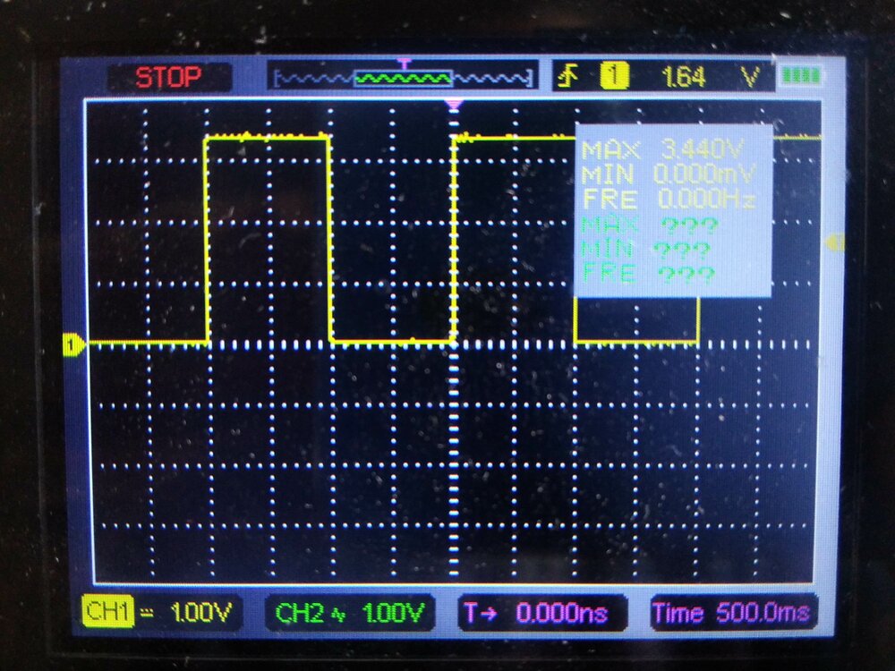
The signal is really clear, we see the HIGH and LOW as expected.
Signals
With an Oscilloscope, I can analyze complex signals. I watched this video to have a better understanding of the main signal I'll be facing (and to practice my Spanish too ^^).
As I have two channels on this oscilloscope, let's try the I2C protocol that has two lines, one for the signal, and the other for the clock. First, let's write a code that sends a signal. Of laziness, I asked ChatGPT to write it to me.
#include <Wire.h>

void setup() {
  Wire.begin(); // join I2C bus as a master
}

void loop() {
  Wire.beginTransmission(8); // transmit to device address 8
  Wire.write(42); // send the 101010 byte
  Wire.endTransmission(); // stop transmitting
  delay(1); // wait for 1 millisecond
}
I connected the SDA and SCL pins of the board to respectively to channel 1 and channel 2. Here is the result:

If we look at the SCL signal (in green) each square of the grid is a period of so if I count the number of squares for the clock and the number of peaks in the SCL signal I can find the period of the clock.
And so the frequency and it's exactly the default I2C bus clock speed!1 [1]:https://learn.adafruit.com/adafruit-esp32-s2-feather/esp32-s2-bugs-and-limitations].
But with the SDA signal (in yellow), I'm struggling to find the 101010 binary number (that means ). The peaks should be equally spaced, but it's not the case. I find the signal not really "square".
Design final project board
Global schematic
I'm starting with the power. I plan to use a battery as I already have a 24v brushless DC motor. It'll be connected to an Electronical Speed Controller (ESC), I want to use a VESC controller as it's open-source, and understand I2C protocol to communicate with the main MCU board.
This VESC will give power to the brushless motor () and to an electromagnetic clutch that will allow me to disengage the motor from the wheel when there is no more battery. This will be controller also with a Relay by the MCU.
The MCU will get its from a regulator. Then it will speak to different modules in different languages:
With the I²C protocol:
- The VESC (Don't know which model yet)
- OLED 4 Pin 128*64 Display Module (SSD1306)
- Gyroscope & Accelerometer 6-axis Module (SEN-MPU6050)
With the SPI protocol:
- Magnetometers 3-axis Module (SEN0419/BMM150)
- LoRa Transmitter Receiver Module (RF SX1276)
Simple digitalWrite LOW/HIGH:
- a 24v Relay Module (HW-482)
Thanks to the Mermaid plugin in Docusaurus I'm able to quickly draw a diagram of all the components/modules and their connections.
Inside the MCU board
Then I zoomed in and drew a schema that shows all the connections I need on the board. I refer to the video I saw before to know all the types of pins needed for each protocol. And I also look a the datasheet of the modules I already have.
Let's design the Schematic of the board
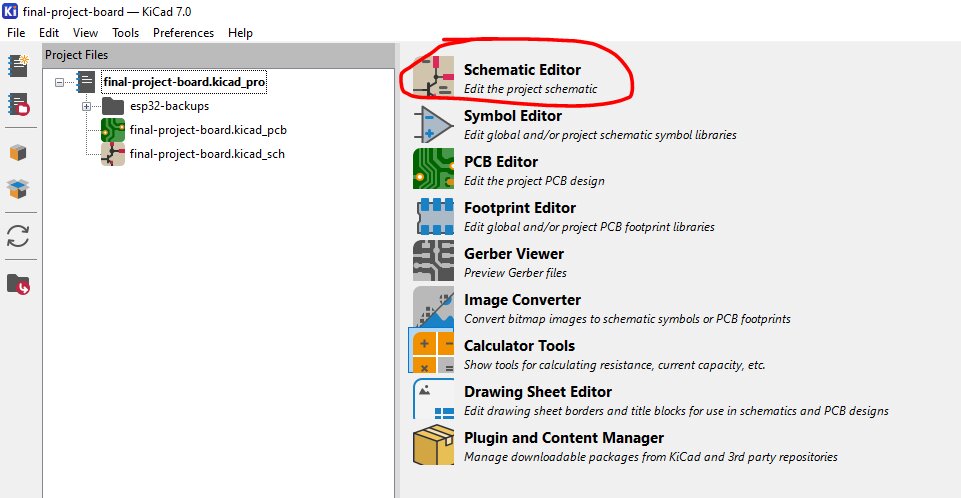
For that I'll use KiCAD, so first I created a new project (File > New project). And open the Schematic Editor.
Then I clicked on Add a Symbol (A) and looked for the XIAO ESP32C3. I've already added the KiCAD libraries durant the local lecture, I found them here.

Then to easily connect the component I added a label to each pin of the ESP32C3 board and also added the 3 power symbols (+5V, +3.3V and GND).

I didn't want to forget so I also edited the page settings to add some info.

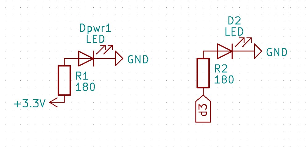
I will add 2 LEDs on the board, one sees when the power is on and the second shows interactions (connected to d3 pin). As they need a 20mA current to work with Ohm's law I had to add a resistor equal to . I don't have this value, so I will put a resistor.
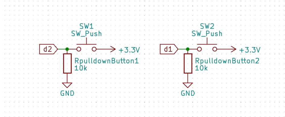
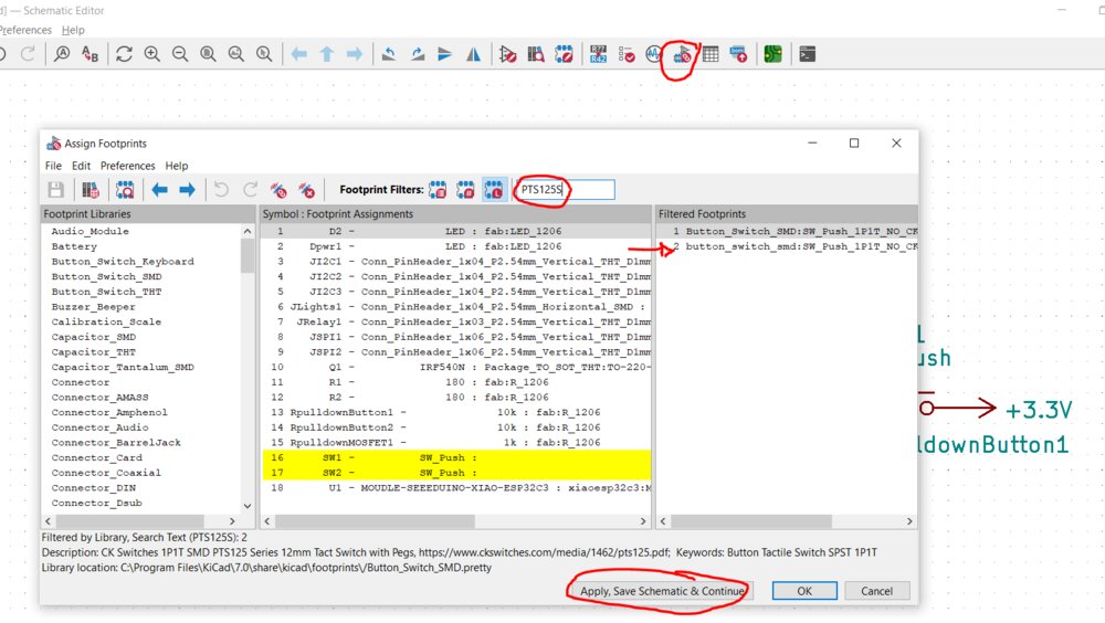
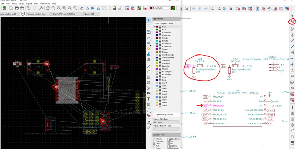
Then I want 2 buttons to be able to increase or decrease a value, or to connect the Bluetooth for example. I don't have the buttons from the Fab Academy inventory. I have two big buttons with a 12mm square shape. I found the footprint in this librarie. It's the Tactile switches SMD package from the PTS125 Series. The name of the library is SW_Push_1P1T_NO_CK_PTS125Sx43PSMTR. For now, in the *Schematic Editor** I'll just add a SW-Push symbol, and I'll link it to the footprint later on. I want their value to be 0/LOW by default so I added a pull-down resistor of , as explained in this video.
Now I will add the Relay's pin. I need 3 pins (+5V, Signal and GND). I don't have SMD pins, so I'll choose a PinHeader THT with hole diameters of .
It's the same for the I2C with 4pins (SDA, SCL, +3.3V and GND) and 6 pins for the SPI connections (MOSI, MISO, SCK, CS (same as RX on the XIAO EPS32C3), +3.3V, and GND). Once all pinheads and their labels are connected, I can use the Highlight wires and pins of a net function to check each connection.

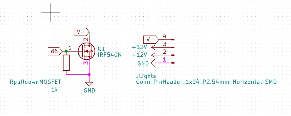
The only pin left from the board is the TX pin. It can be used as as DigitalPin too. So I decided to use it with a MOSFET to turn on and off the lights of the trike. I guess I'll have 12v lights, I'll use an IRF520N Mosfet that I have. I just copy the schematic more or less of this MOSFET module. I just changed the order to not have a 12 Volts jump and removed the LED.
 source eelectronicparts.com
As the footprint of the IRF540 and IRF520 are the same, I used it on the schematic to go quicker.
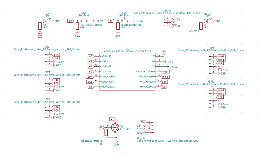
Here we go the full schematic.
I run the footprint assignment tool. Most of the Symobols are already linked to a footprint, the only ones that were missing are the two switch button. I looked for them and assigned them to the right footprint.
Create a PCB
Now I switch to the PCB Editor and Update the PCB to add all the components in the Editor.

After checking if they were any errors, I had all the components on the screen. I quickly saw that the footprint for one of the LEDs was the wrong one. So I went to change it and re-update the PCB. The components are grouped and I see the line between the connection I've declared on the schematic.
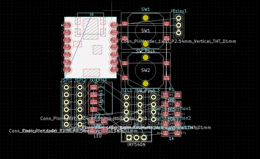
I move the component around following more or less the schematic, as I've already looked for the place for those components. I nice trick is to use the *Highlight wires and pins of a net function of the Schematic Editor Window, and I can see the pin the PCB highlighted too. As I work with 2 screens, is convenient to work with both windows.
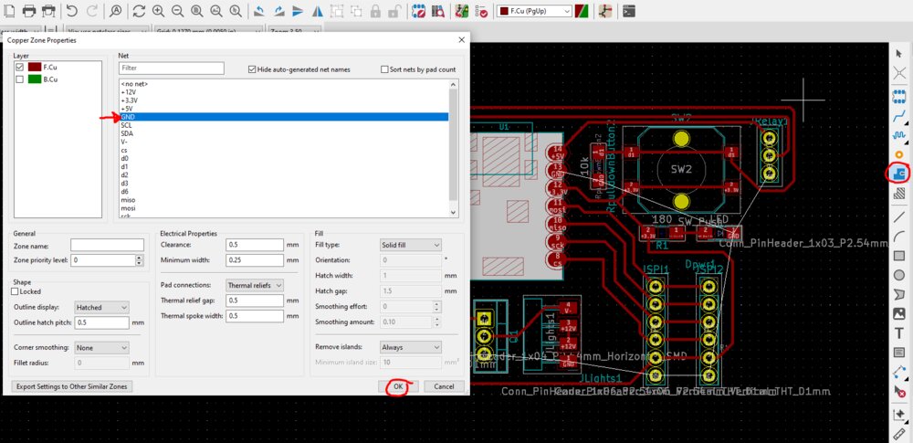
When I am happy with the position I can start the routing. But first I wanted to check the Width of the track and the clearance. For that, I went on * > Net Classes*
I use this track calculator to choose a width for the 12v track. I have a thickness for the copper of and will be more than enough for some 12v lights. So a track with should be ok. For the MCU connections, I decided to stay with the we used for the local lecture.

So I use the route track tool to link physically all the components. I connected everything, except the GND connection as they will be connected by the filled zone.
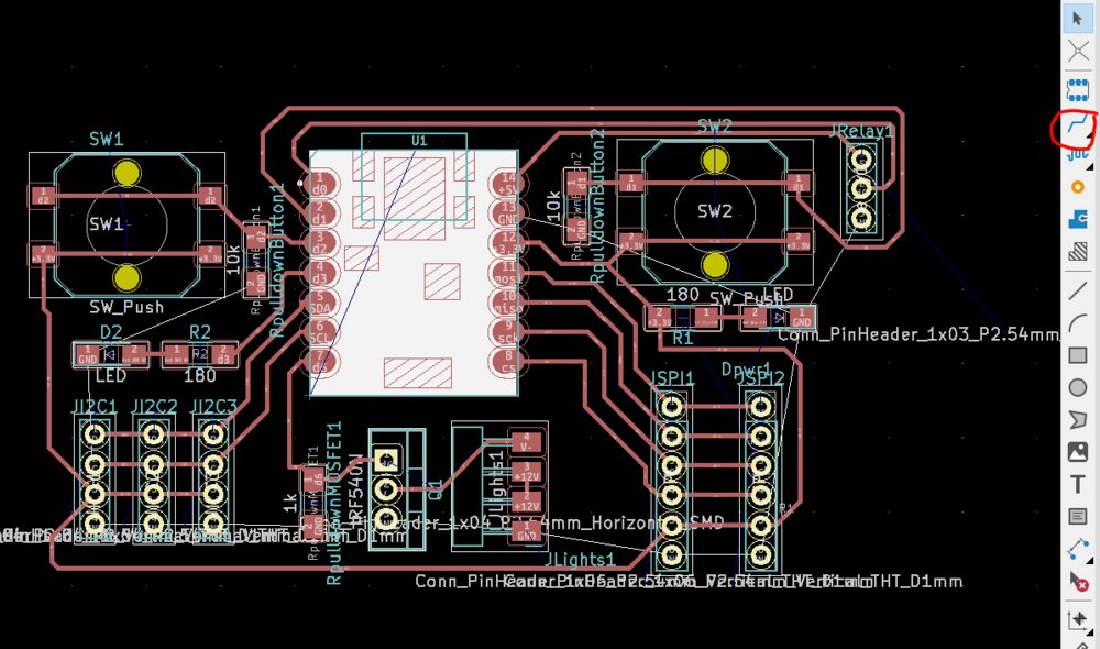
I see that I already gonna have some problems with the ground connection for the MOSFET. But anyway, let's try to finish. So first I define a filled zone for the ground, and then a square in the Edge Cut layer.
When it's done I can run the DRC (Design Rules Checker), as expected the ground doesn't touch all the components it needs to.

So first, as the button has 2 pins connected in pairs, I will use them as "jumps". And second I'll pass the +3.3V from the top.
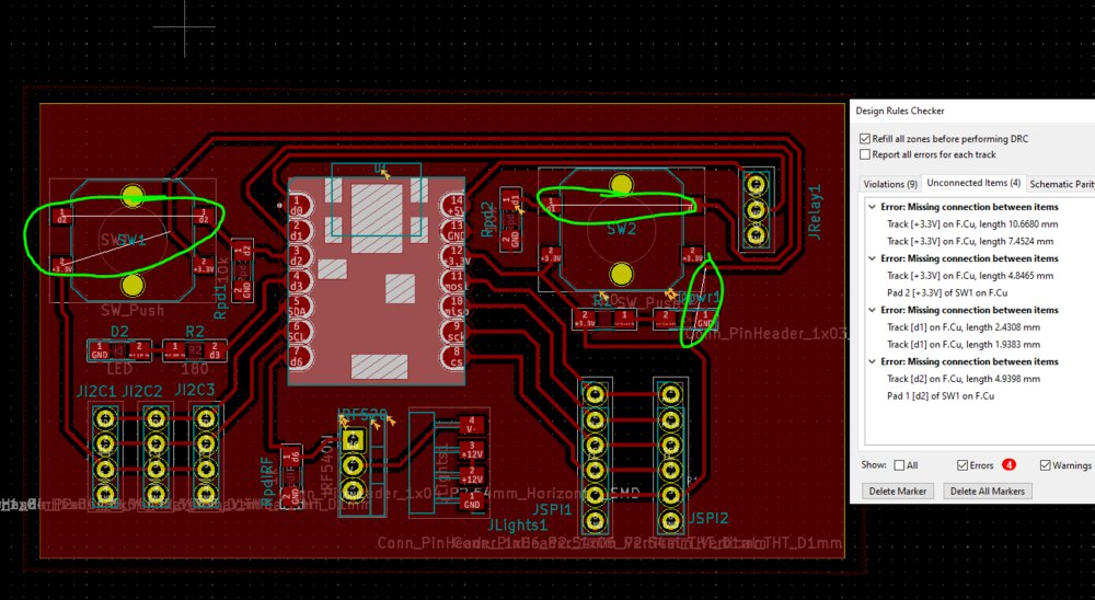
It's better, but now, the DRC doesn't that the button to have pins connected and that I can act as a jump.
Edit a footprint
The circular pad for soldering the connection is not that good. So I tooked the advice of Ahmed, the instructor, and I decided to change mine for an oval shape of x . For that, I can select the PinHead I want to edit, and go to Edit the footprint. There is select the pad by clicking on it and changing the shape and the measure.
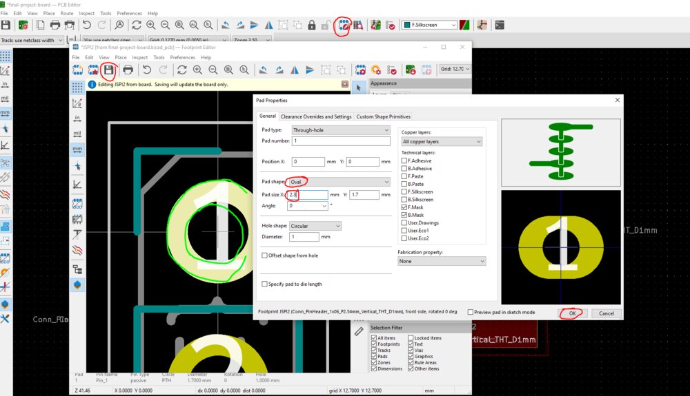
I pushed the change from the first pad to all the other ones.

After I decided to do an Edit the Footprint library so the changes apply on all pads from the board, after a Tools > Update Footprints from Library...
Then I added 4 holes to fix the board somewhere. After that, I wanted to have a look at the Gerber files. So I did a File > Fabrications Ouputs > Gerbers (.gbr)
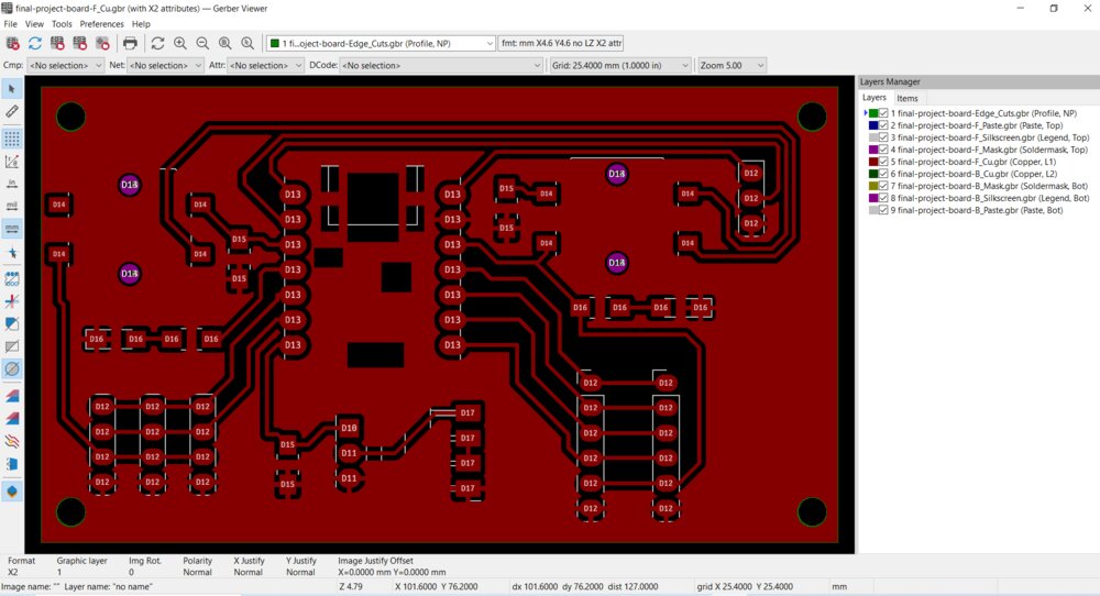
I can see already the milling operation. Can't wait for the Emmbedded production week =).
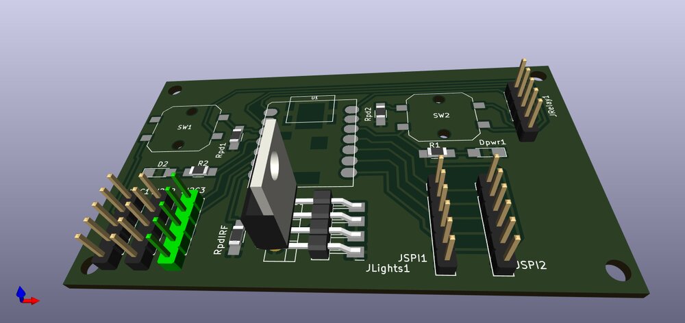
The result
So here a 3D view of the PCB. I already see some problems, for example with the pads for the Lights, not sure they will be secured enough.
Files
Here are the files for the week.