WEEK09 - Output Devices
Following the design of week_06 and the production of week_08, this time I had to design an additional board. But also I was really unhappy with my board from last week. So I did everything again from scratch. I have had a couple days to recover and also to consider why I am struggling so much with electronics.
I hadn't really touched it before, or at least not since high-school, and struggling so much the week before was really bothering me. I don't like failing challenges. Alas, after some conversations with friends, some pancakes, and some considerations and sketches I decided to try again. This time I wanted the board to be better though, I wanted everything to be better, and also, I wanted to pin out ground and power and all more often, since I had realized that to be able to attach the input and output devices I had to consider the GND and power pin-outs in my original board design.
WEEK NINE ASSIGNMENT
| Assignments | Completed |
|---|---|
| GROUP | |
| - measure the power consumption of an output device | GROUP ASSIGNMENT PAGE here |
| INDIVIDUAL | |
| - add an output device to a microcontroller board you've designed, and program it to do something | - done |
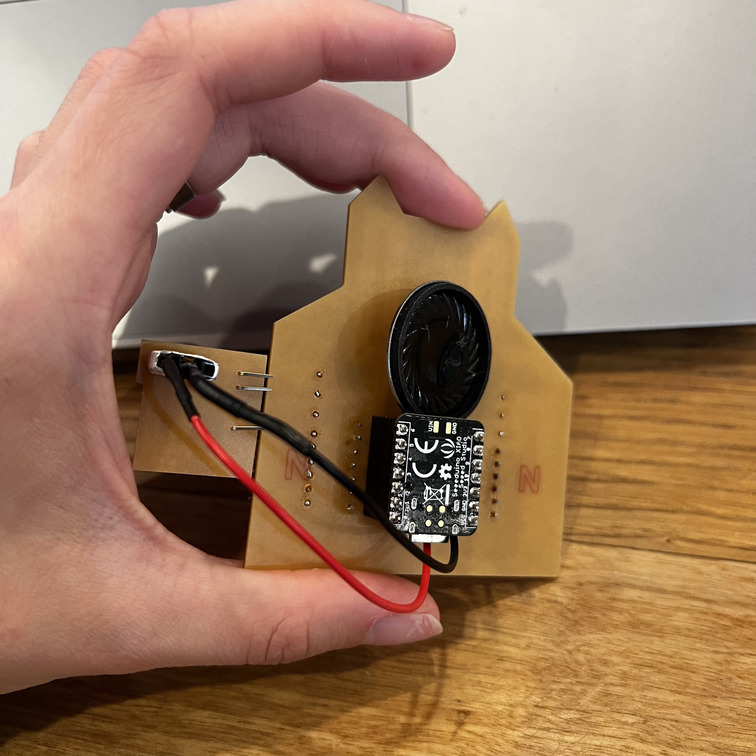
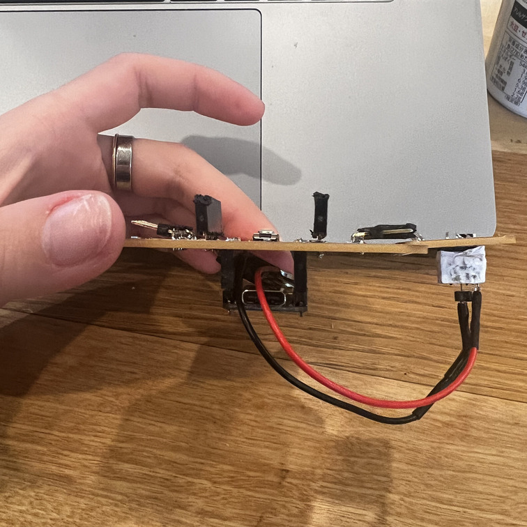
HERO-SHOTS
GROUP ASSIGNMENT
You can find this here. \ I learned in the group assignment that whilst you can use a multimeter to measure the powerconsumption of some outputs, you should better use an oscillator.
THE PROCESS
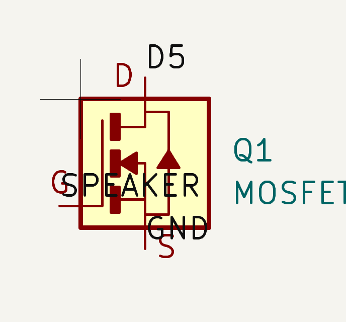
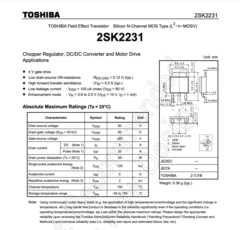
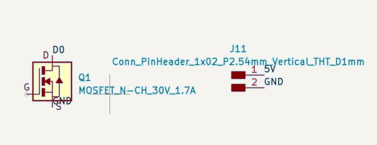
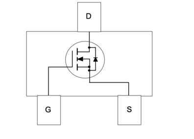
For this output week I decided I wanted to use a speaker as my output device. So my board had to feature a transistor. I choose a mosfet. it has three legs which are as follows:
DRAIN: leads to the speaker GATE: leads to the microcontroler pin SOURSE: leads to GND
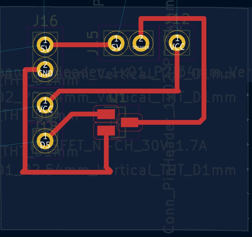
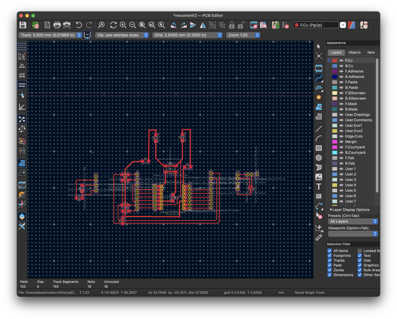
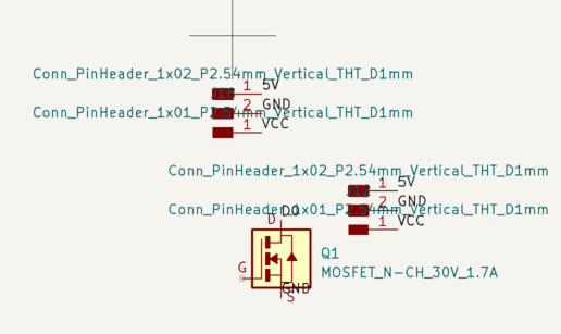
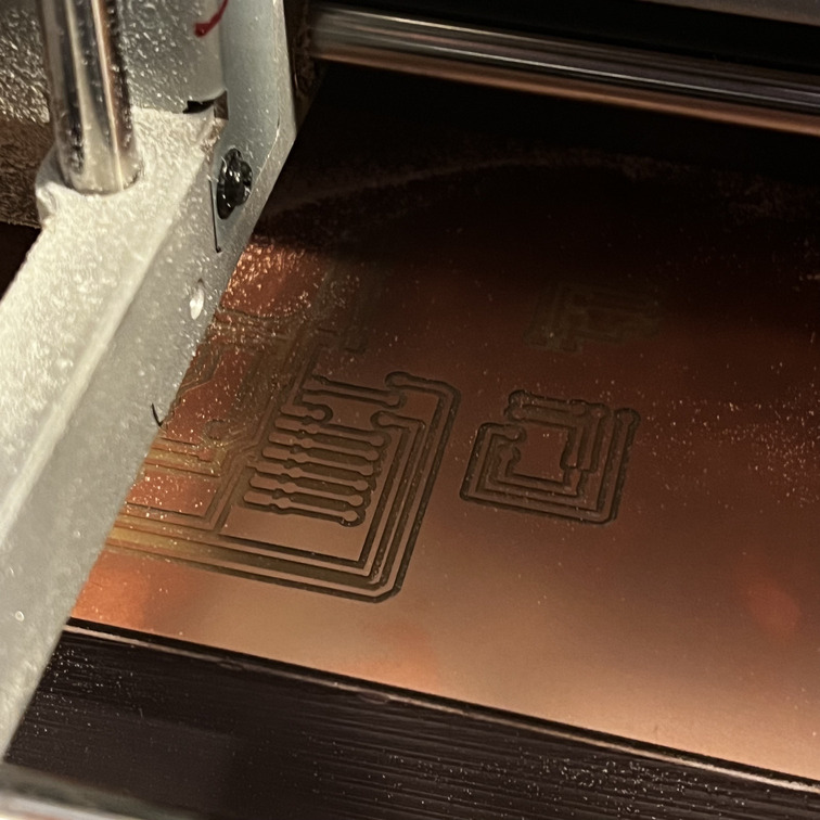
DESIGN: THE NEW BOARD
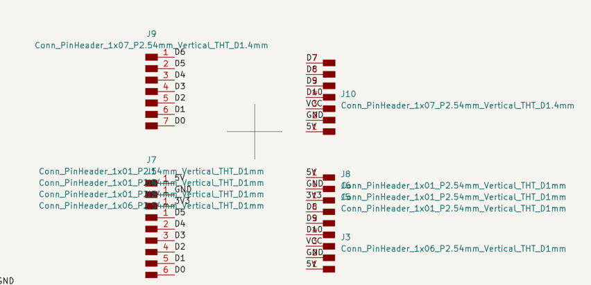
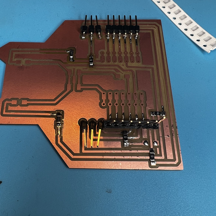
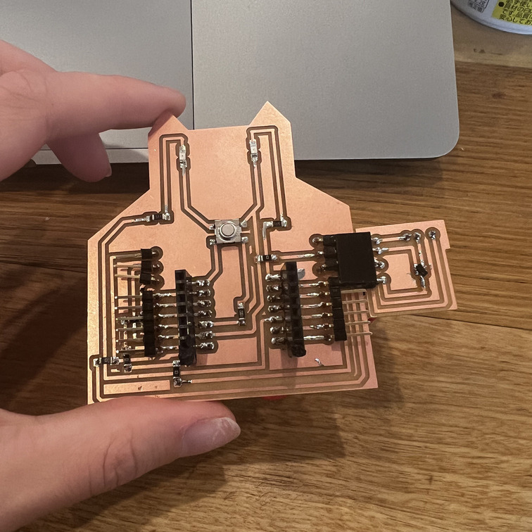
Also since the board I made previously was not as good as I would like it to be, I decided to redesign it and to also break out PWR and GND in many more directions multiple times. Now they are broken out 4 times, and can also be broken out additionally towards the back of the board.
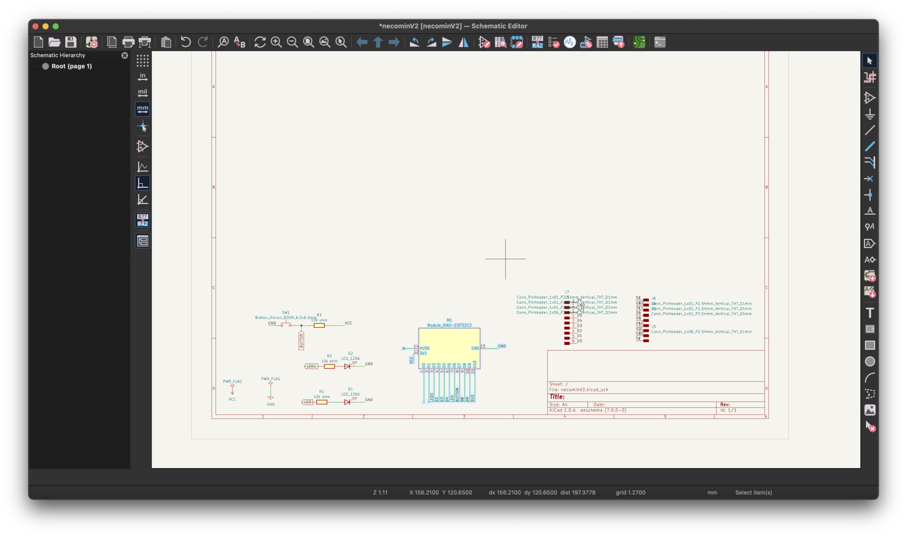
Then I designed and finished all elements
DESIGN: THE OUTPUT DEVICE
I also created additional schematics for both the output board for this week and also the input board for week 12, since I already knew what I wanted to do
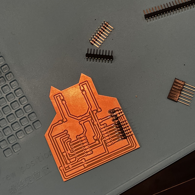
SOLDERING
After last week I paid special attention to the soldering. Really making sure to apply a lot of heat.
CODE
To do some alternating sounds this was the code I used, with the help of my instructor: Later on in week 12 I changed the code more towards what I wanted once I started using the input device as well.
const int spPin = 5; //XIAO RP2040

void setup() {
pinMode(spPin,OUTPUT);
}

void loop() {
  //hz1000();
 toneOut();
 // pwmSound();
}

void hz1000(){
  digitalWrite(spPin, HIGH);
  delayMicroseconds(500);
  digitalWrite(spPin, LOW);
  delayMicroseconds(500);

}
void toneOut(){
//tone(pin, frequency, duration Usec)
  tone(spPin,261.626,1000000000);  //c4
  delay(1000);
  tone(spPin,329.628,1000000000);  //E4
  delay(1000);
  tone(spPin,391.995,1000000000);  //G4
  delay(1000);
}

void pwmSound(){
  //analogWrite(spPin, 255);
 analogWrite(spPin, 150);    // low volume??
  delayMicroseconds(500);
  digitalWrite(spPin, 0);
  delayMicroseconds(500);
}
MISTAKES, FAILURES AND LESSONS
These electronics weeks have truly been the hardest for me so far. Every week has taken double to triple the amount of time that it should, and I don't even know how to address it into time-management as I'm not sure what to cut. If I stopped any of the tasks mid task, they would just remain undone.
MISTAKE ALERT!
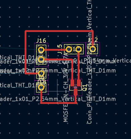
As much as I improved this week, I still ended up making a crutial mistake regarding the output board. Despite looking at the datasheet of the MOSFET I still managed to somehow make the connections to the wrong legs. I managed to remedy this during soldering by turning the transistor upside down and building little solder mountains for it to sit on... but for the future I also made the adaptations and changes to the initial board design, in case I ever want to mill it again.
CHANGES
This the fixed design: