WEEK06 - Electronics Design
This week we focused on designing a personal computer-board which would be able to communicate with an embedded micro controller like a XIAO esp32. This was my first engagement with electronic circuits since highschool, as this was very different to any kind of electronics I have touched in the past 10 years.
This board did work in the end, just in time for the lecture, BUT i still chose to re-do it completely in Week9!!! So please also view that board and documentation in terms of electronics design AND production.
WEEK SIX ASSIGNMENT
| Assignments | Completed |
|---|---|
| GROUP | |
| - use the test equipment in your lab to observe the operation of a microcontroller circuit board | GROUP ASSIGNMENT PAGE here |
| INDIVIDUAL | |
| - design a development board to interact and communicate with an embedded microcontroller | - done |
| - extra credit: try another design workflow | - done |
| - extra credit: make a case for it | - |
| - extra credit: simulate its operation. | - |
HERO-SHOTS
GROUP ASSIGNMENT
We started the day with our group assignment, which was was to observe the operations of our microcontroller circuit-board. You can find it here
DESIGNING A PCB
- Install, launch KiCad
- Add the fab library
- Eeschema
- add components
- annotate components
- electrical rule check(ERC)
- associate components with footprints(CvPcb)
- generate netlist
- PcbneW
- import netlist
- design PCB
- design rule check(DRC)
- export images for milling
To help me figure this process I followed multiple tutorials.
KiCad 6 tutorial from Fablab Kamakura: here
Kurumi Shiowaki's 2021 Documentation here
KICAD
SET UP: Download KiCad for your operating system. Get the Fab Library from here
Moved to file in Documents > KiCad > 6.0 > Libraries (I created this folder) > Fab (I renamed)
Open KiCad and Preferences > Manage Symbol Libraries. --> I followed the instructions on the Fabcloud for this.
CREATING A SCHEMATIC
Time to create a schematic
open schematic editor.
look at hotkeys
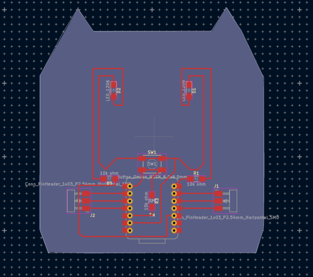
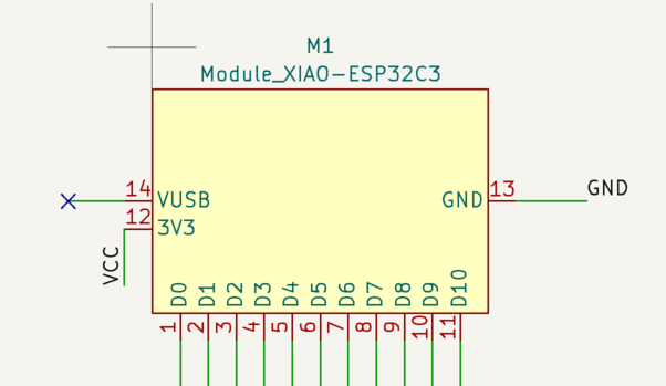
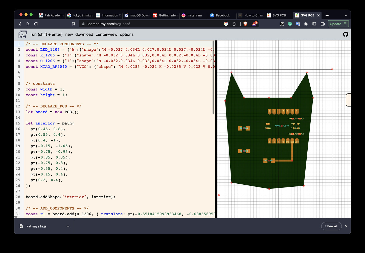
Start placing down components: For this week I wanted to make a board that would interact with the xiao esp32 micro controller. I wanted to shape the controller like a cat with two LED's forming the eyes, and a button for a nose which would trigger the LED's. I also wanted to break out 6 pins on each side which would look like whiskers.
To create this circuit I required the following components:
You add component by pressing A
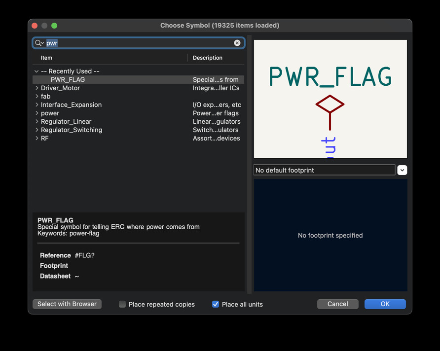
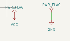
PWR_FLAG
VCC = On the xiao board the 3 volt power input/output is a 3v3 port. I renamed/labled it to vcc so that I could more easily follow the pre-existing tutorials.
GND = Ground
In the symbols directory you will also see a folder named fab. Ensure that you are taking the actual bit's components from there.
For me electronics was a new thing to confront myself with, so I struggled with understanding which components were needed and how I should visualise circuit digitally, without knowing first which compontent I needed and what their purpose was.
XIAO ESP32 BOARD
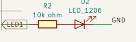
LED
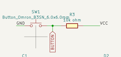
BUTTON
for each LED and button you need a:
RESISTOR (10k Ohm) : You give value to the resistors by placing your cursor insise the symbol and pressing V
This is what and LED looks like:
This is a button looks like:
WIRING THE BOARD
To wire the compents together, put your curser int he circle of one icon, and draw a line to connect it to the other icon by pressing W.
Label all ends L. The programm knows that everything that is labled the same is wired together.
Add a 'no connection flag' to anything you wish to leave untouched on purpose.
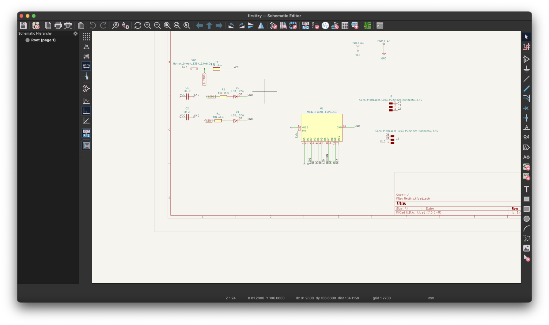
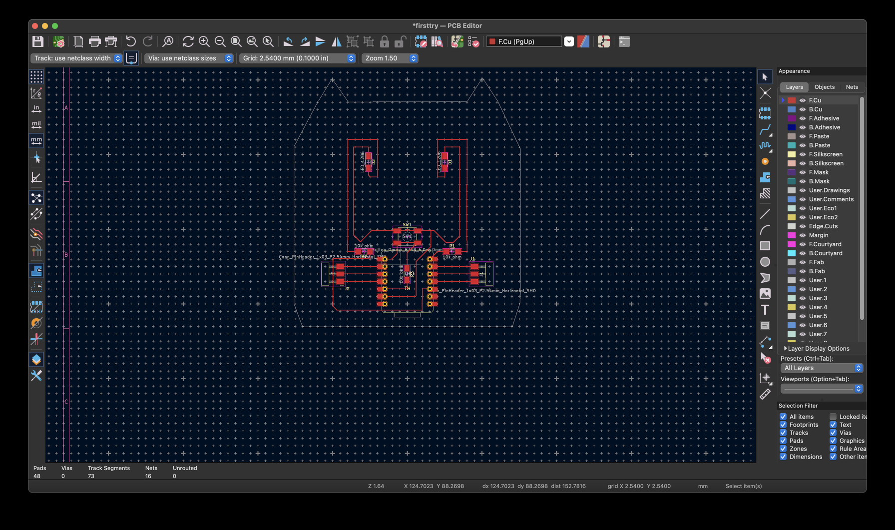
FINAL SCHEMATIC LOOK
As you can see it's
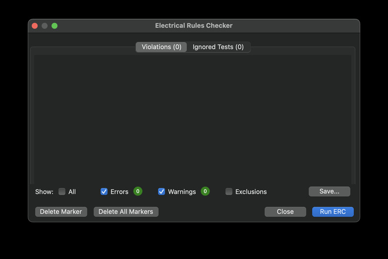
ELECTRONIC RULE CHECK
To do the electronics rule-check, click on the checklist icon in the top right-ish corner of the schematics editor.
 Passed with flying colours.
After this open/send the schematic to the PCB editor
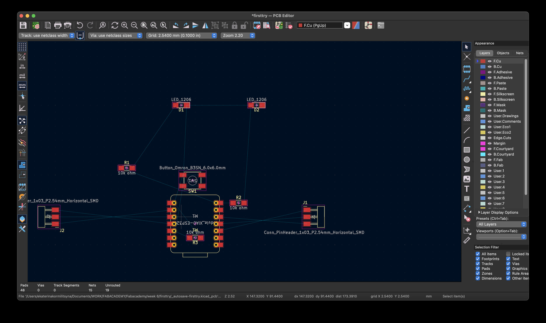
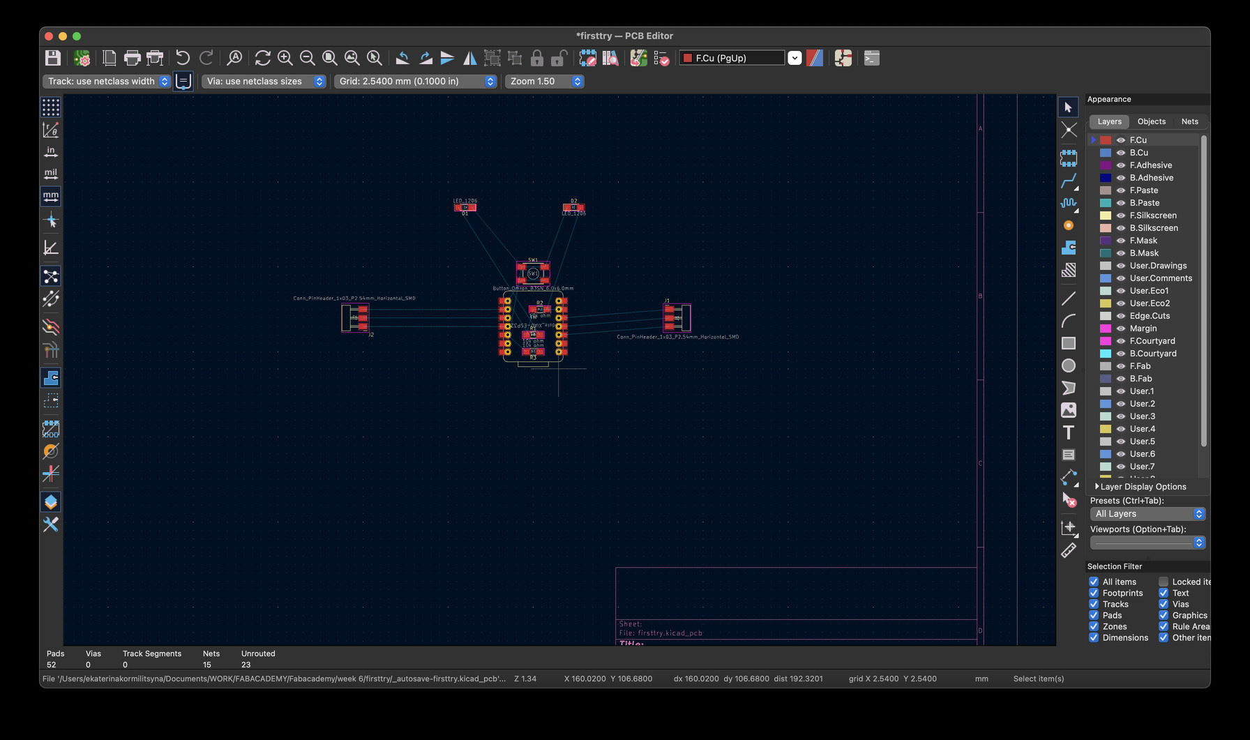
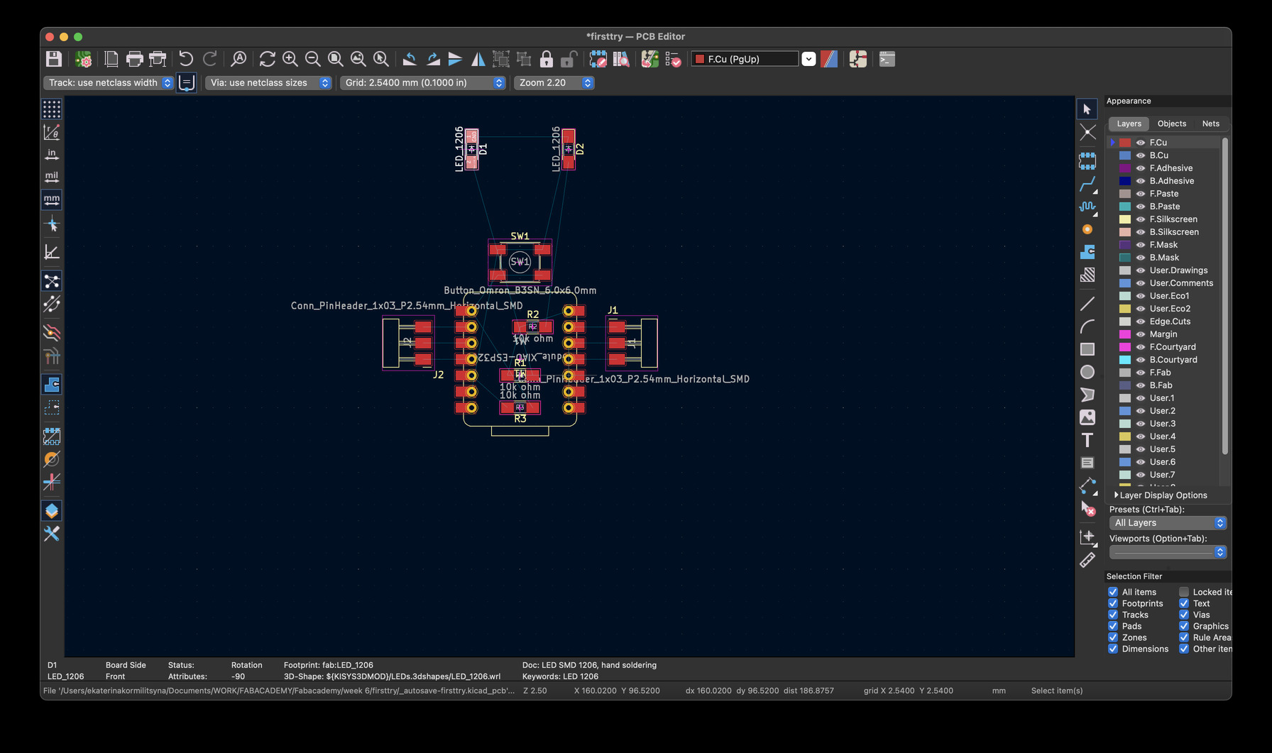
PCB EDITOR
I have been playing 'connect the dots' on IOS whenever I'm on the subway for the past 2 years... this reminded me alot of that, and thus was quite a pleasant experience.
Basically just connect all the ins and outs that you labled in the schematics. This is the step where you can acctually have fun and make shapes and design the board. Keep in mind, nothing should cross.
Same interface rules apply as in the schematics.
IF THERE IS NO SOLUTION: if you cannot solve the puzzle add an extra resistor (but with 0k Ohm!!!) to your schematics. Then you can use this as a bridge to permit wires to cross.
Keep your eye on your wire/track path ticknesses, once I milled my board I realised that some had been too narrow to survive the milling process.
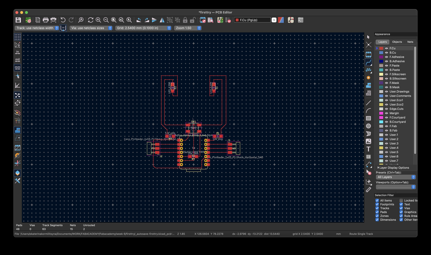
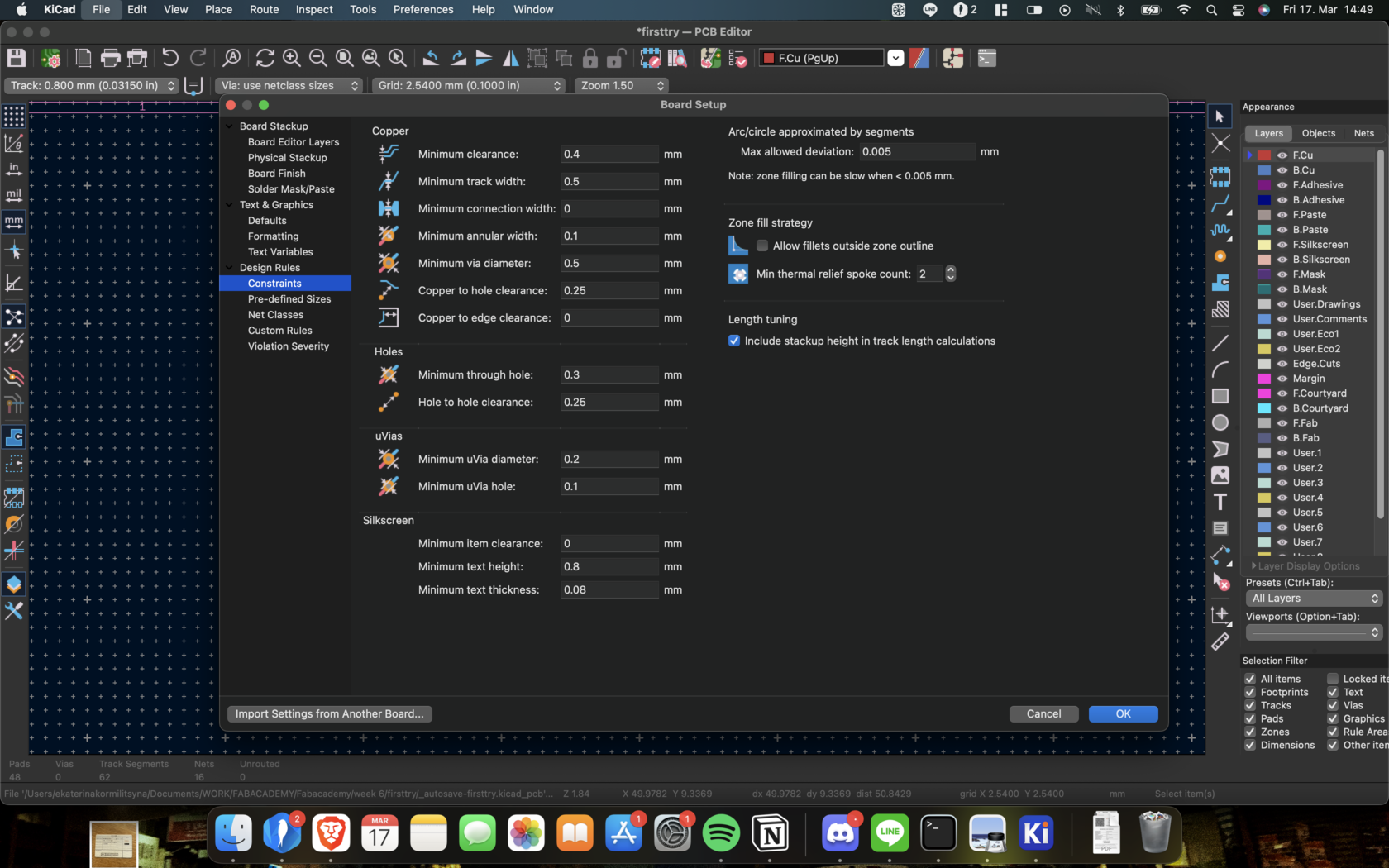
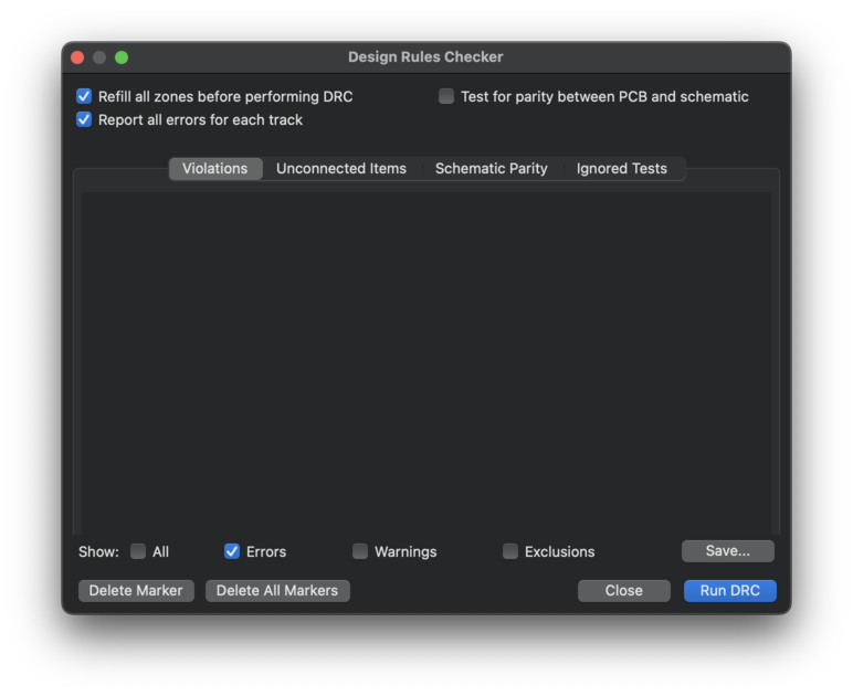
DESIGN RULES CHECK
To make the design rules check I first had to define which design rules I wanted it to be checking for. This meant I already had to know some things about my milling machine and process. So inside of KiCad I defined some design constraints. I go further into this during week8.
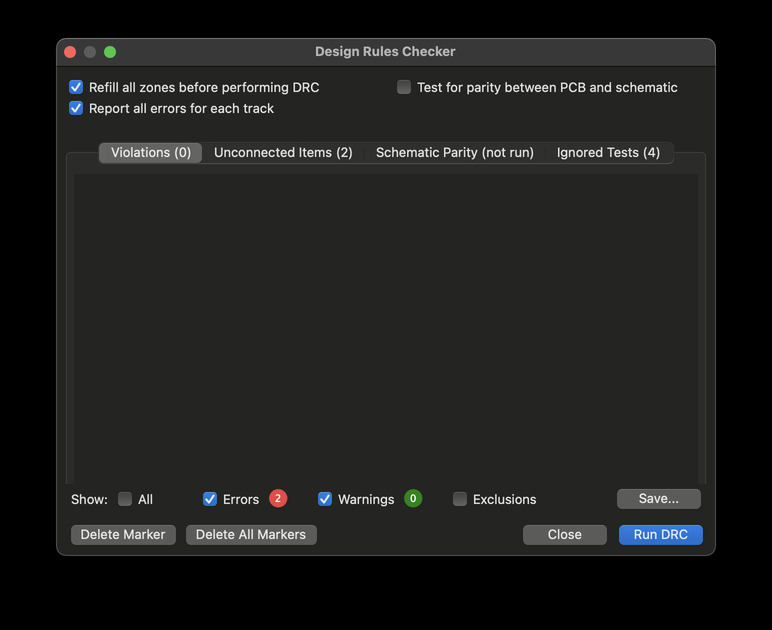 I originally kept getting two errors about LED's not being connected, even though they were. I later realised that this was because I had labled both LED's and their pins the same name: the programm didn't like that.
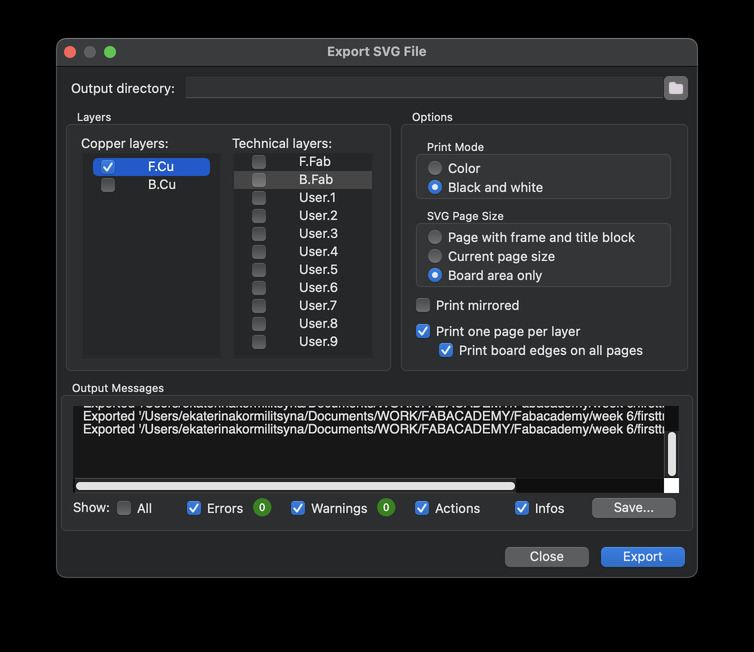
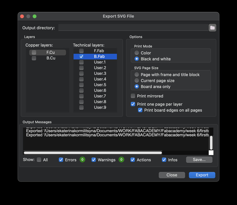
EXPORTING THE BOARD
After making a board outline and a board polygon (i am still not fully sure if it's necessary because I did not end up using it for mods, or when prepping board for the milling machine.)
But this is how to export: ( do each layer seperatly just in case)
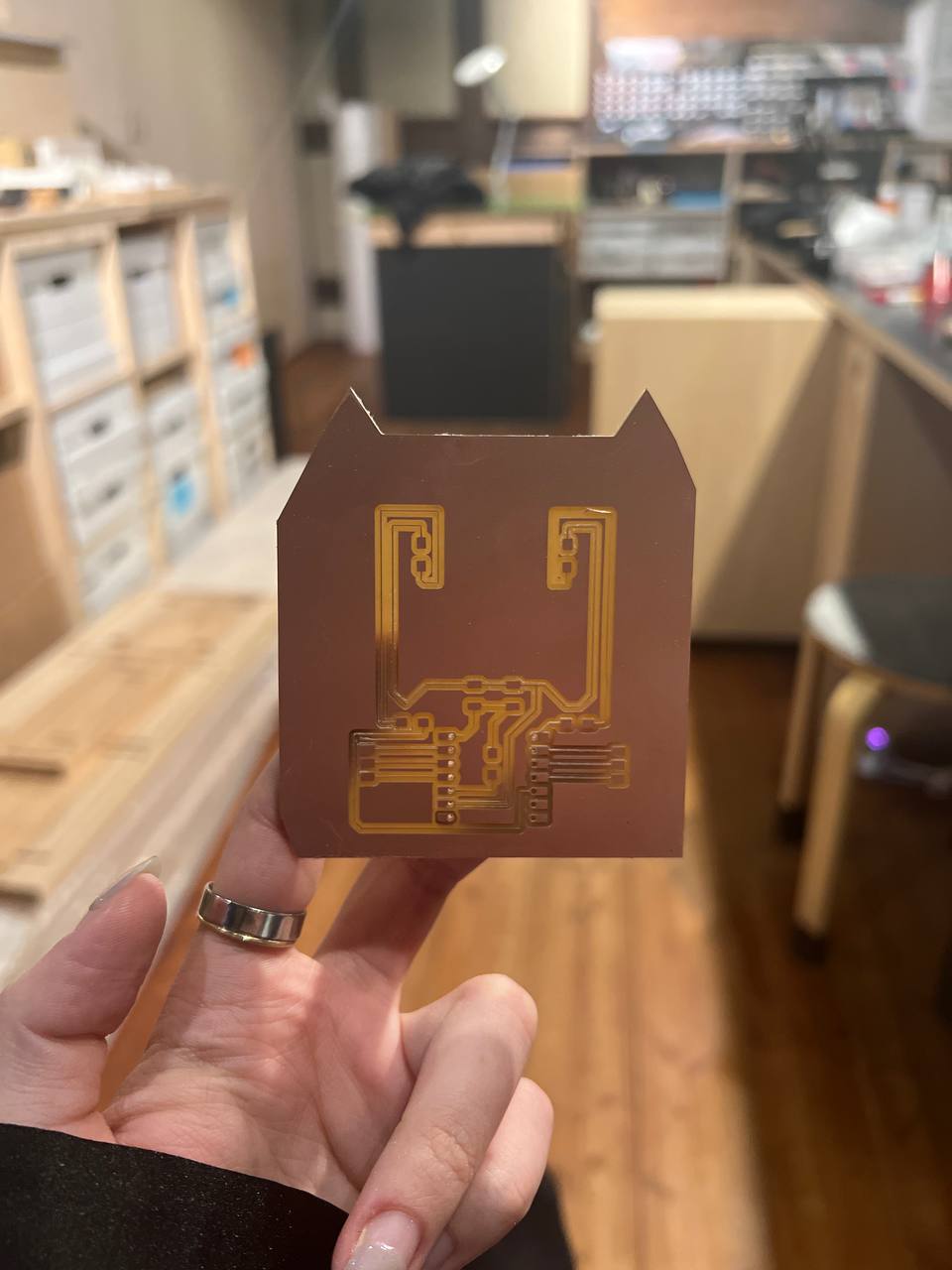
After you've exported the board you then go to a program called mods, where you then prep the board for milling by calculating the pathways for the cnc-mill. This was a rollercoaster.
But I did manage to get a board. In a way- milling the board and testing it is also a type of design-check- maybe even the most thorough one.
THOUGHTS AND NOTES
Thoughts on pulling this week before electronics production. It does make sense, but it should still be aimed to mill a board this week, I think. If I had not milled my board I would not have realized some things that the design-rule check doesn't highlight. Most importantly the track widths and the track proximities and shapes.
Overall this process also showed me, that if you know the board that you are making you could also design it visually only, using illustrator or SVG PCB.
Once I continued the process after exporting, I faced a lot of issues on my computer related to mods, and illustrator when it came to inverting colours. I think this is a graphics issue, as my own files were not causing the same problem on other people's computers.
I liked KiCad. I think because it was the first software I learned for this it's ok, and yes the overall movement and interface is made for a mouse and key-board combo. but it kind of reminds me of video-games so it's fine.
But I do think, if it exists for Ipad, that KiCad would be great to use with a touchscreen capability.
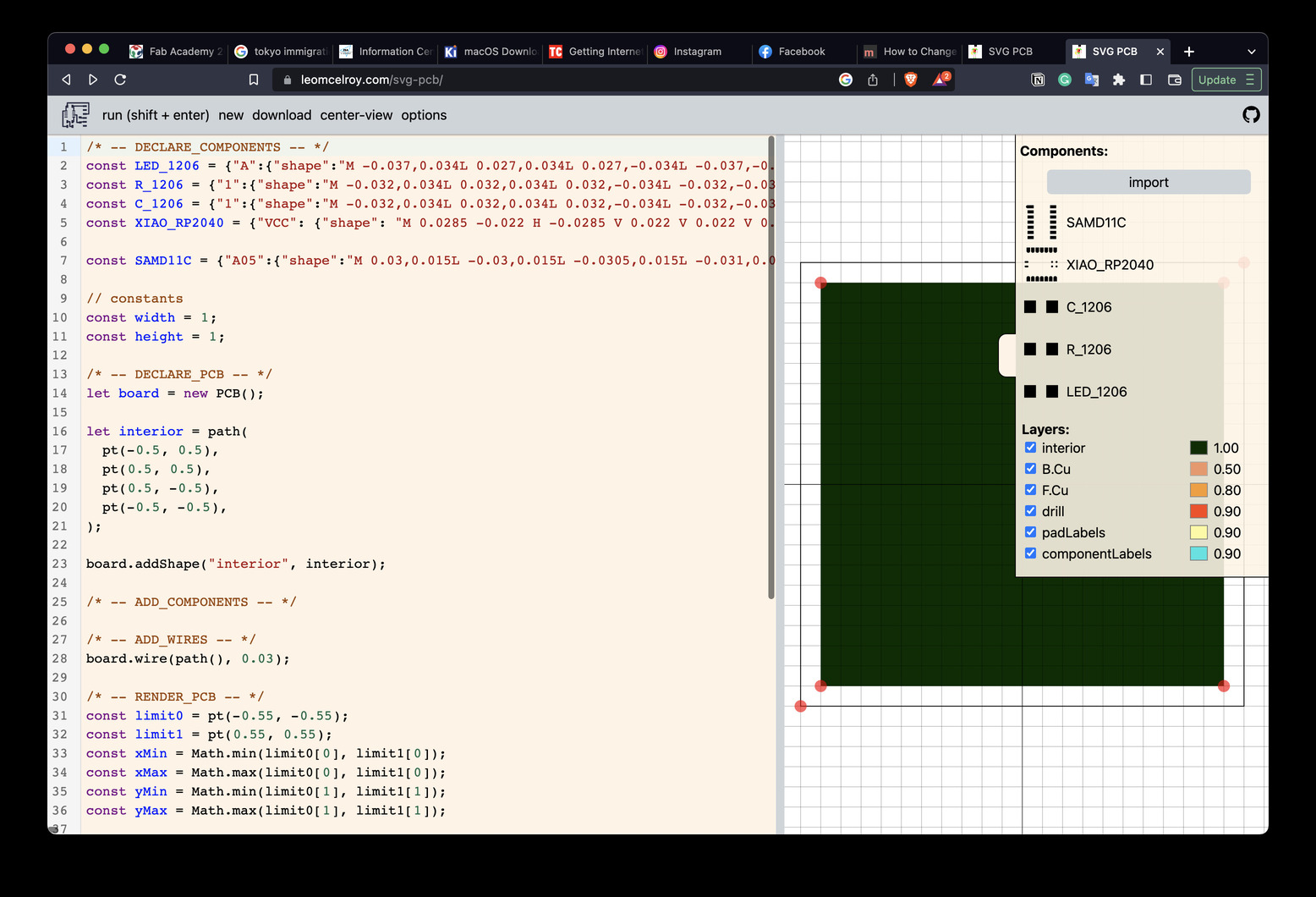
SVG PCB
We allocated around 30 min to also try SVG PCB. This pcb editor was actually quite usueful because it also functioned on both a code and visual basis, however it unfortunetly doesn't have an electronic or a design rules check build in.
It can be accesed here: PCB SVG and is made by the same person as GRAM- which was a program I explored in week 2.

FILES
KiCad
SVG-PCB
SVG-PCB file.zip (you can drag this into the editor)