7. Electronics design
Task: Electronics Design
- Group assignment:(Page Link is Here)
- Use the test equipment in your lab to observe the operation of a microcontroller circuit board (in minimum, check operating voltage on the board with multimeter or voltmeter and use oscilloscope to check noise of operating voltage and interpret a data signal)
- Document your work to the group work page and reflect on your individual page what you learned
- Individual assignment:
- Redraw one of the echo hello-world boards or something equivalent, add (at least) a button and LED (with current-limiting resistor) or equivalent input and output, check the design rules, make it, test it. Optionally, simulate its operation.
Electronic production week.
I am confident in this week because I am very interested to learn electronic design.
Our instructor Yadu Sharon introduced about use of different components in a circuit and how to design a circuit. that helped me to remind basics and to make a clear idea about this week.
I also watched some YouTube videos and read some blogs about circuit designing.
Then our mentor Gogin Francis talks about Ecad software. And he explained how to design a PCB with fusion 360.
Tasks:
- Schematic design
- PCB design
- PCB milling
- Soldering
- Programming
I learned about Uses of some common electronic components, that is given below
- *Resistors* It resists the flow of current by dissipating electric power as heat.
- *Capacitors* The function of capacitors is to temporarily hold electric charge, and release it whenever more power is needed elsewhere in the circuit
- Inductors They store energy but instead of storing electrostatic energy, inductors store energy in the form of a magnetic field that generates when current flows through them
- Diodes It is a device that allows current to flow in one direction only, from the anode (+) to the cathode (-).
- LEDs LED is a diode that emits light when electricity passes through it.
- ICs ICs, or integrated circuits are exactly that, they are circuits and components that have been shrunk down onto wafers of semiconductor material
-
Transistors A transistor is a semiconductor device used to amplify or switch electrical signals and power
ref: www.seeedstudio.com
For PCB designing I used Fusion 360 ECAD.
Make schematic design
What is the schematic diagram of a circuit?
It can be described as a circuit diagram or the functional diagram of electronic circuits. Symbols are used to represent components and show how they are connected electrically.
ref: www.edrawsoft.com
The steps are given below.
- Open fusion 360, go to File → New Electronics Design
A new window will open now.
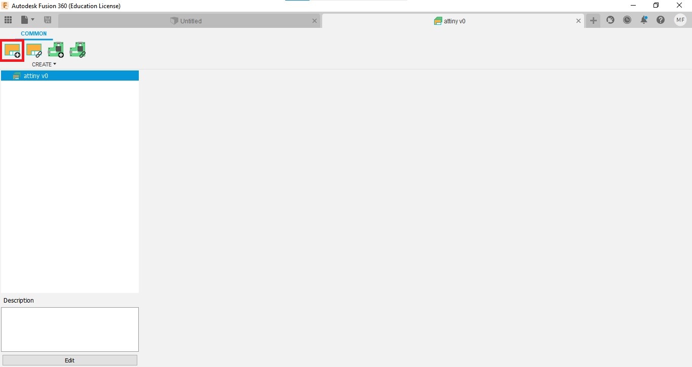
-
Click on New Schematic Design Icon, a new tab will open now.
Add library
Fab academy provides a library that includes most of the components we have to use.
After cloning that library to the computer, Go to Library Pane, and click on Open Library Manager icon.
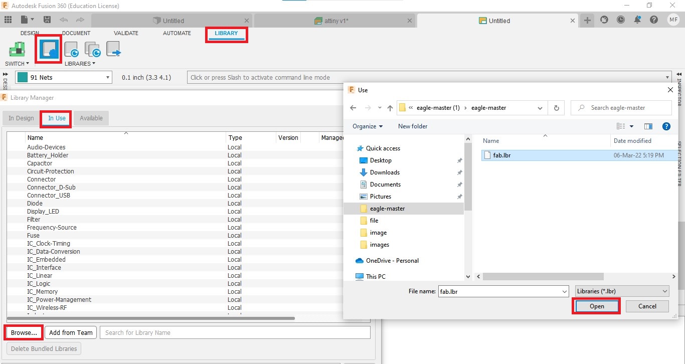
In the opening window, go to In Use → Browse → and open the cloned library, and click on
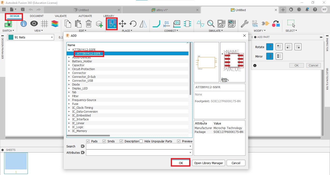
In this week we use attiny IC, But the library provided by Fab academy doesn’t include that file. So I downloaded that file from Saheen Palayi’s documentation.
Create/Edit a component
A 6 pin is needed for this design. But it is not included in the given library of fab.
So I edited a component.
Steps are given.
Go to File → New Electronics Library
In the opening tab, click on Create New Device icon and import an existing file.
I changed the names and add icons and edited the pin and pad connections.
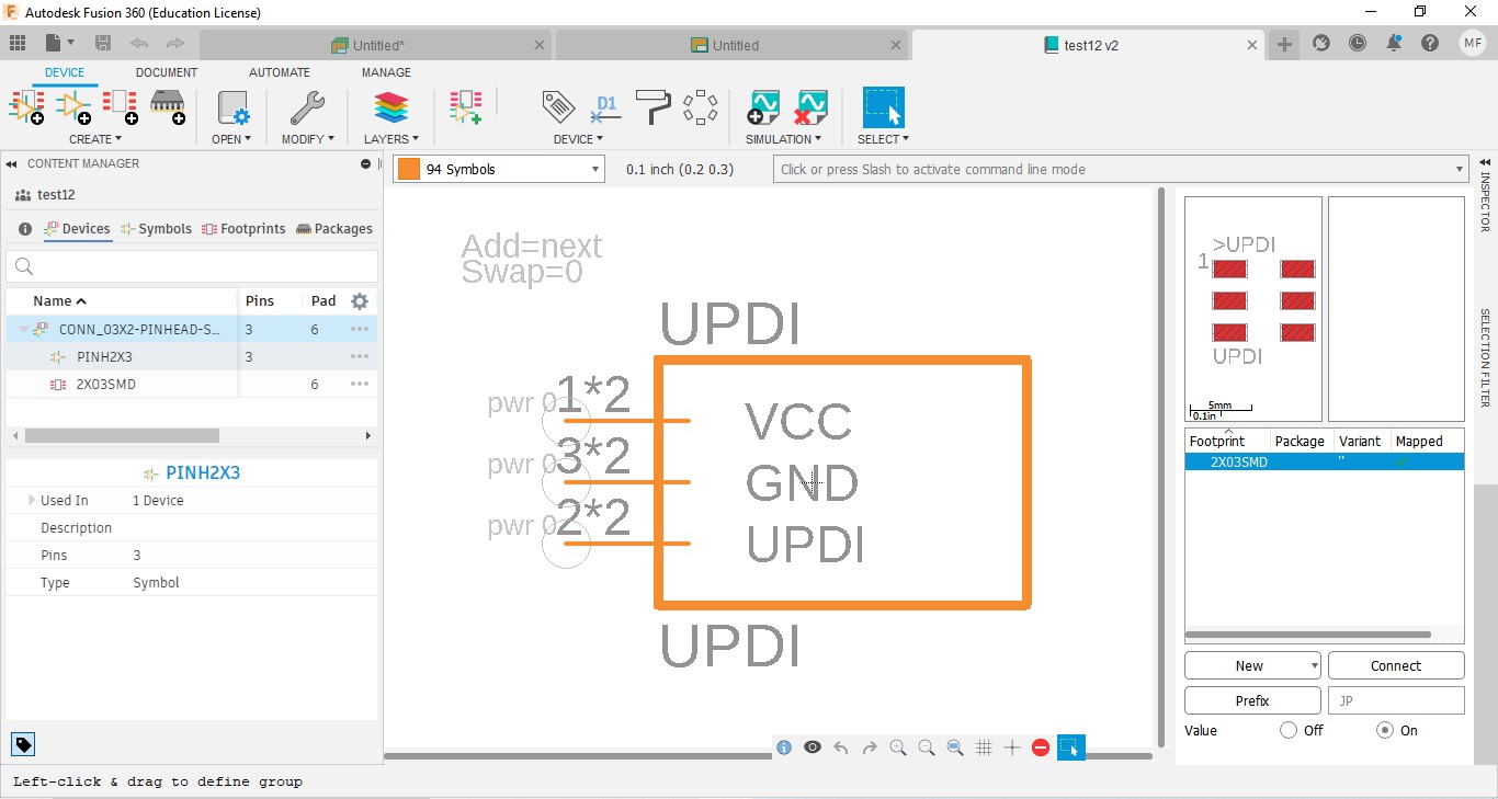
After saving the file, I added the device to the library.
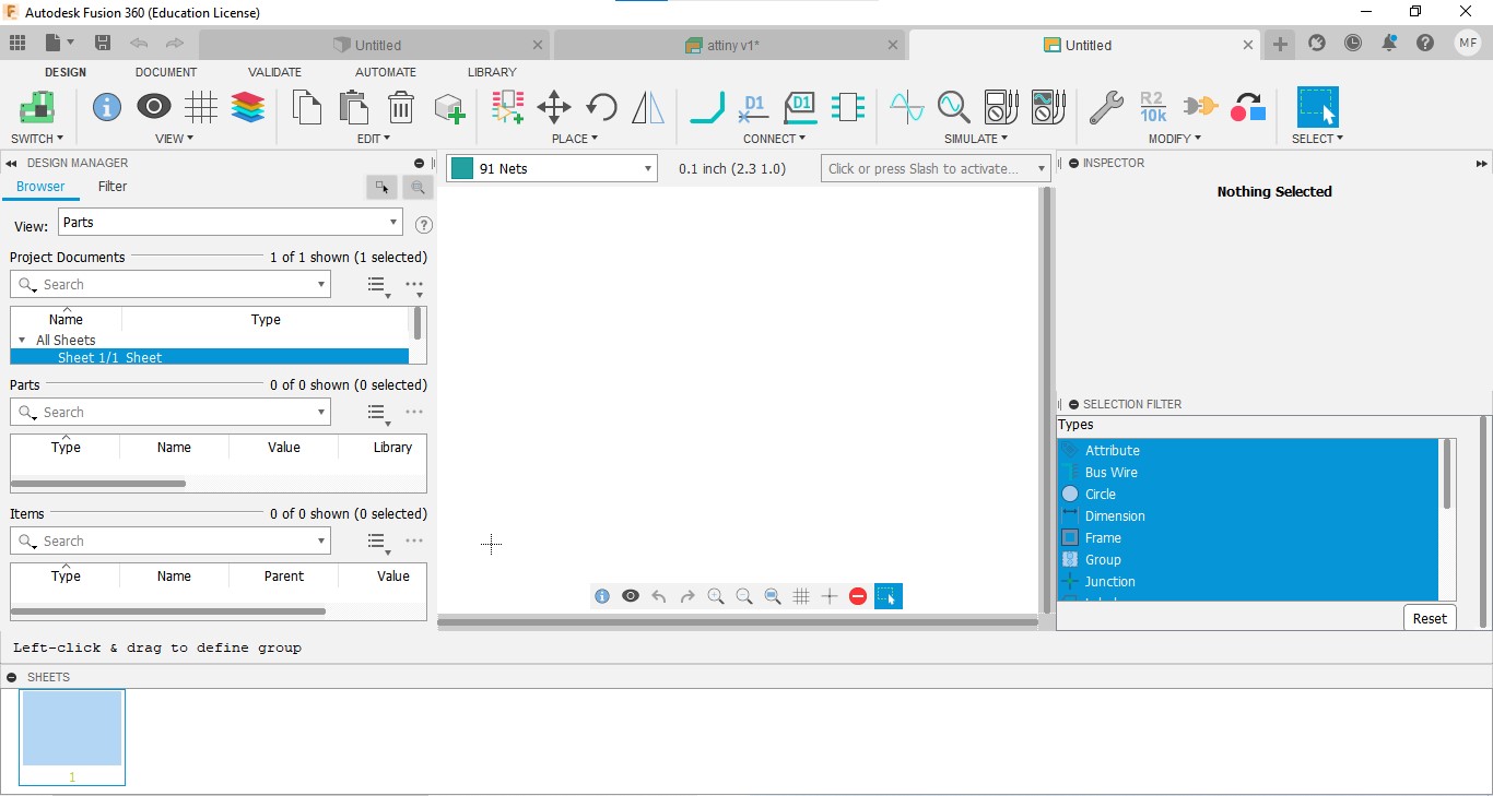
Create a schematic diagram
Go to the Design Pane and click on Add part icon, and I added different parts for the circuit.
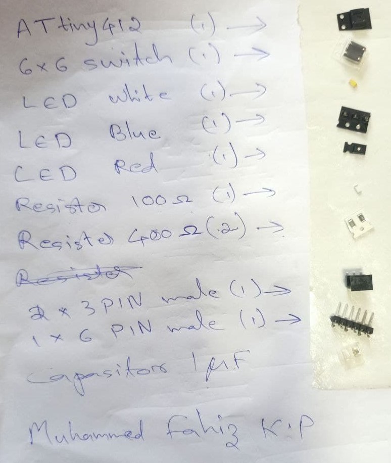
Parts I added:
- ATtiny 412
- Resister 4
- Capasitor 1
- LED 3
Using the move and rotate options, we can position various components.
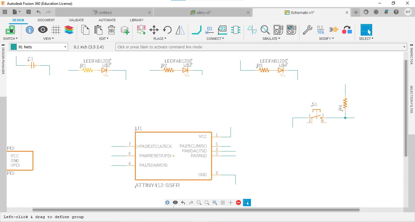
I used nets to link components with the reference image.
And I added a LED and a switch to the circuit.
- How did add LED and a Switch to the circuit? LED: cathode is connected to the ground through a resistor and anode is connected to a remaining pin of the microcontroller. Switch: One pin is connected to the ground and the other pin is connected to a pin of the microcontroller.
Instead of complex wire connections, I used schematic parts like earth and VCC. For some connections, I used the Label tool.
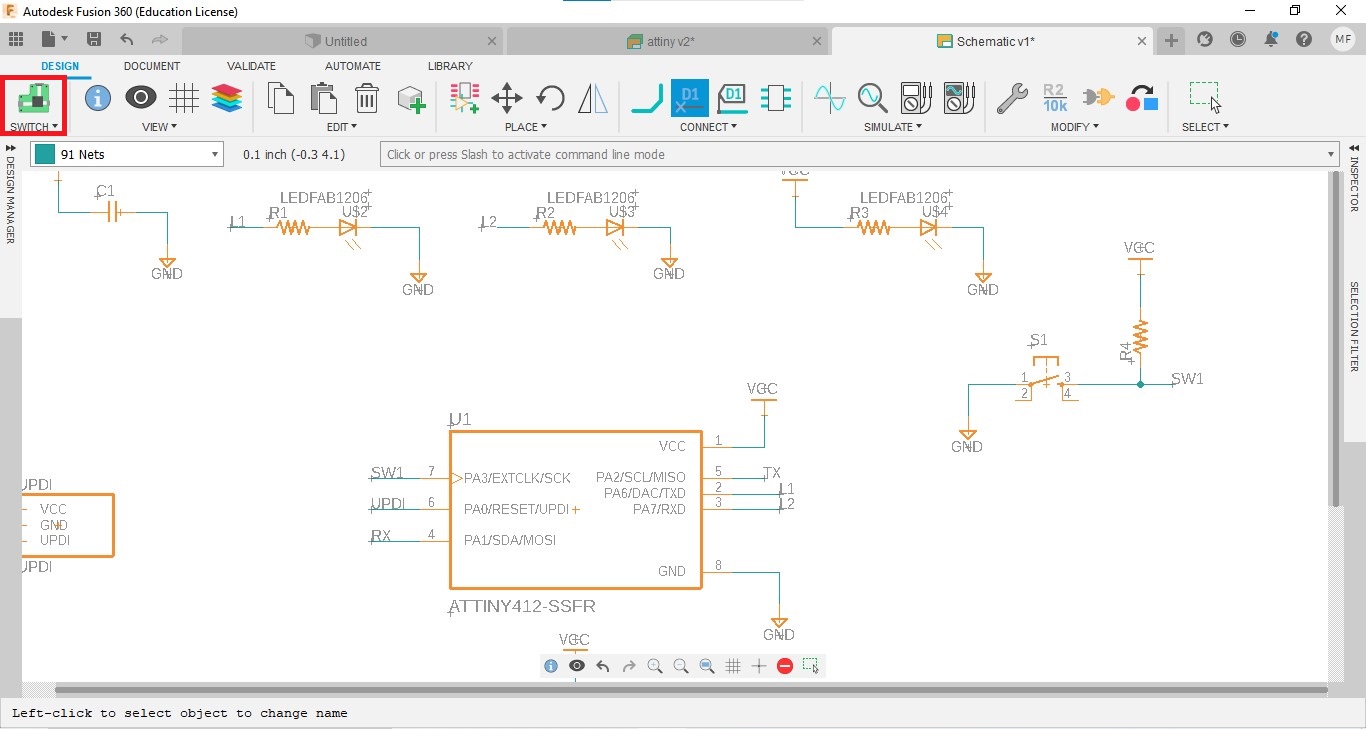
How to add Ground and VCC.
- How to add Ground and VCC? We can use VCC (power) and GND (ground) symbols to connect power and ground instead of manually routing wires across components. Giving directions to up for all VCCs and down for all ground is a good practice.
We can use symbols instead of routing in the schematic diagram. Symbols that have the same net names will ****be connected.
After completing the schematic diagram, click on Switch to PCB document icon (green icon in the top left corner)
In the opening new tab, adjust canvas size and drag and drop each parts inside the canvas.
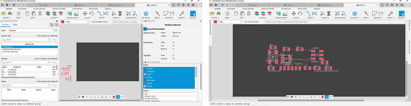
We can arrange each component by using the move tool and rotate tool.
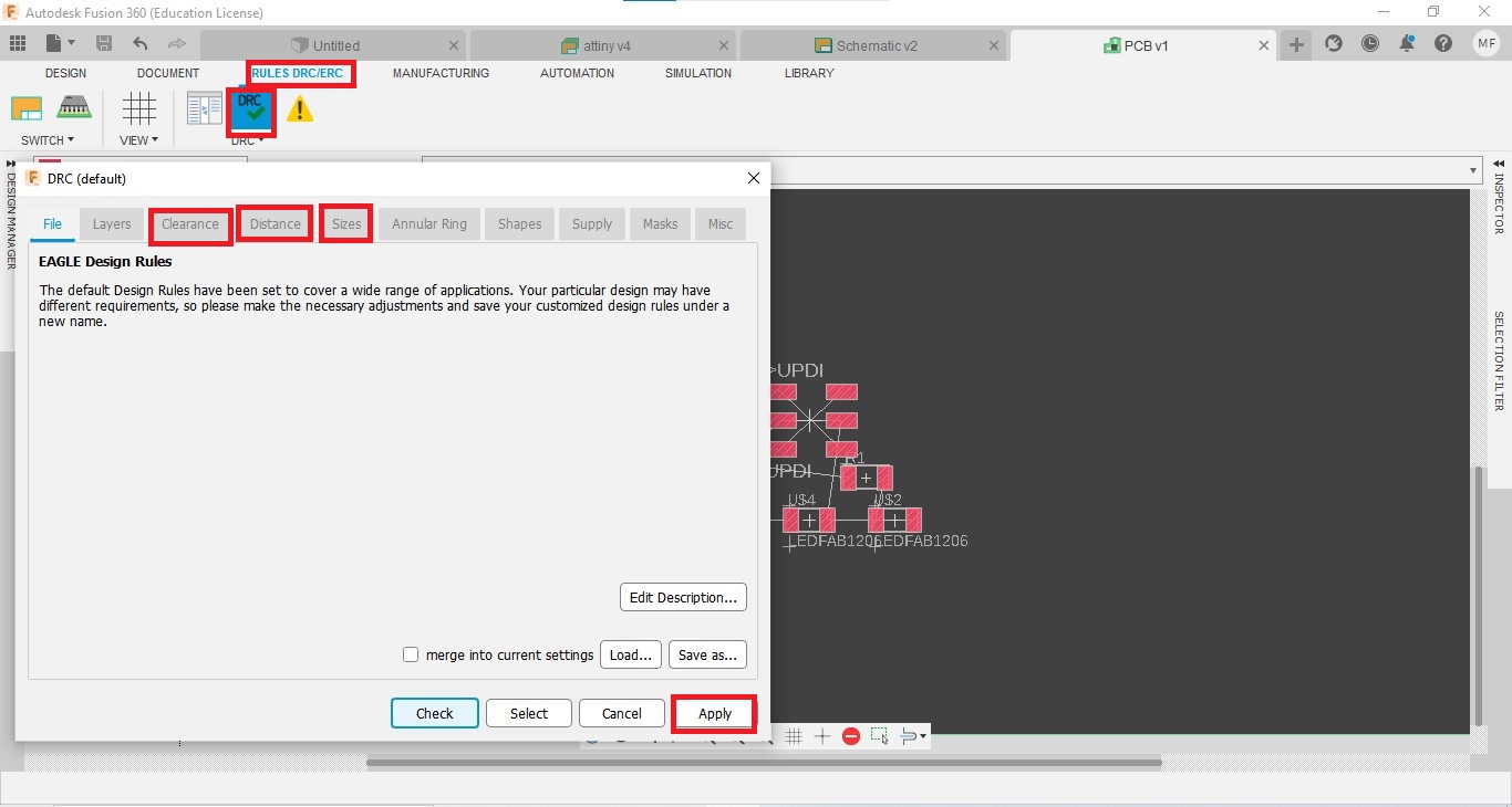
After arranged, Go to the RULES ERC/DRC Pan. and click on the DRC icon.
In the opening window, we can set design rules for PCB milling.
In here we use 16 mils bit and 32 mils bit. I set values like clearance, hole width etc, according to what we find in electronic production week.
After setting design rules, click on apply.
Return to Design Pane. and go to Quick Rout → Auto-route.
In the opening dialogue box, select N/A for all layers except Top. Because we are designing a PCB for solder SMD components.
I selected Effort→ High and click on continue.
In the opening dialogue box, click on Start.
After finishing, we can choose different routes.
I couldn’t get any 100% result. There were some paths without route in my circuits.
So I ripup all wired connections (By go to Ripup → Ripup all) and rearranged components and repeated routing.
I repeat the same process for a long time after arranging components in different ways.
Then I observed the traces and their arrangement. And I manually route some connections
Then I got a best result.
The next step is making export the milling path and cut the path for PCB milling.
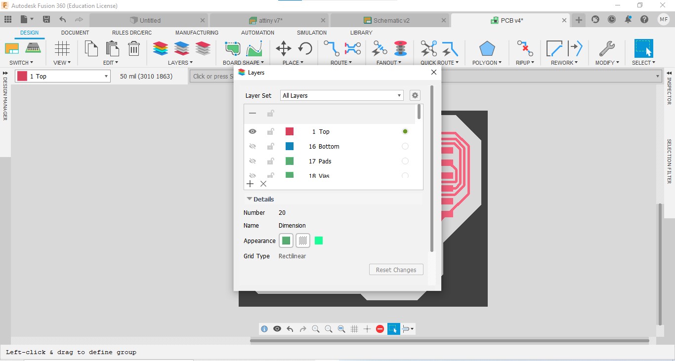
We can hide different layers of the design(route, name, etc.) by go to Layers → Display
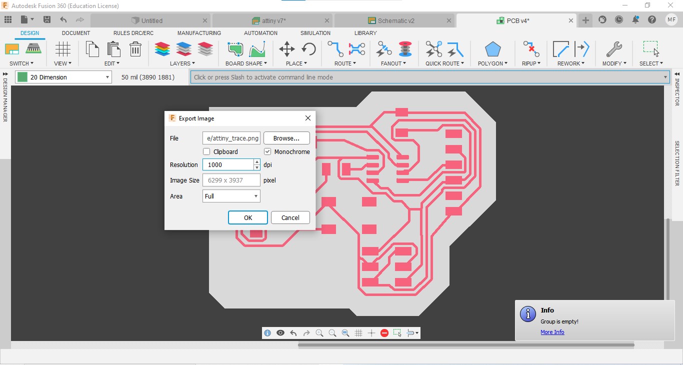
Export milling trace
Hide all layers except the top layer. Type export in the command box and press enter.
In the opening options select image.
In the opening box.
- Specify a location.
- Tick on monochrome
- set resolution 1000.
and click OK.
Export cutting trace:
Hide all layers except the dimension layer and repeat the rest steps.
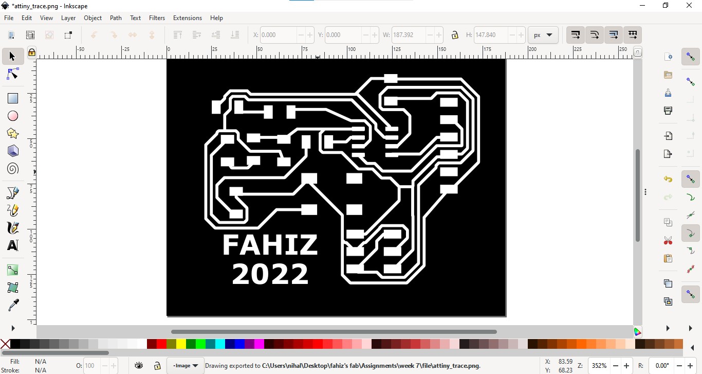
Then I open traces in Inkscape and added my name.
Open the file in Mods and mill the PCB
Finding values for resisters and capacitor.
I included 3 LEDs in my circuit. For controlling the voltage flow, I added one resistor series to each LED.
To find value of the resistor:
$$ R = (Max voltage- voltageDrop)/current $$
In here, Max voltage is the maximum output volt of the ATtiny(It is 5V ).
Voltage drop: Voltage drop is vary for different LED’s(according to color, Brand, etc.)
Current: It is the maximum current throughout the component.
I referred datasheet of each LEDs to find Voltage drop and Current(Just search in google)
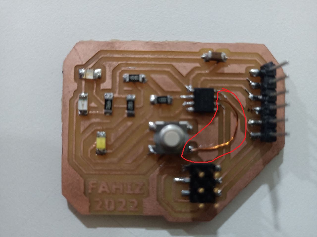
After milling, I collected components from inventory and started to solder.
At that time I noticed that there are some short connections between some traces.
Our mentor Rahul said me to edit DRC values.
I changed the clearance between traces into 18. and I edited some route traces also.
And repeated the remaining steps as I do before.
When I resolder the ATtiny 412 from the board, one leg broke.
So I collect another ATtiny from the Inventory.
After milling that PCB, I found there is an air wire there.
So I decided to continue soldering and add a connection using copper wire.
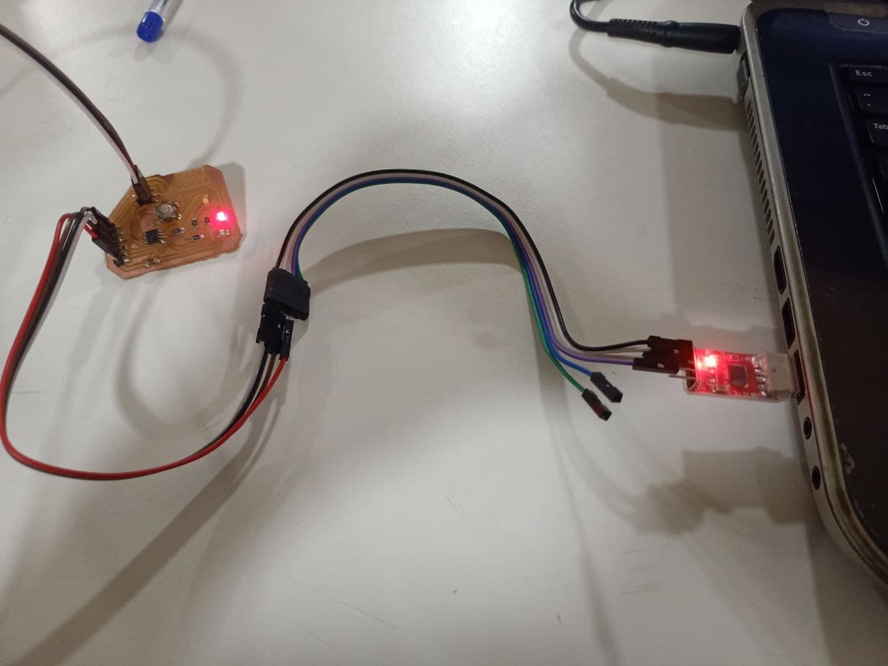
Programming
We are using Arduino software to program the board.
The steps I followed are given below.
Connect UPDI and our board pins using jumper wires
Open Arduino software. Go to File → Preference → Additional board manager URL and paste the code below.
[http://drazzy.com/package_drazzy.com_index.json](http://drazzy.com/package_drazzy.com_index.json)
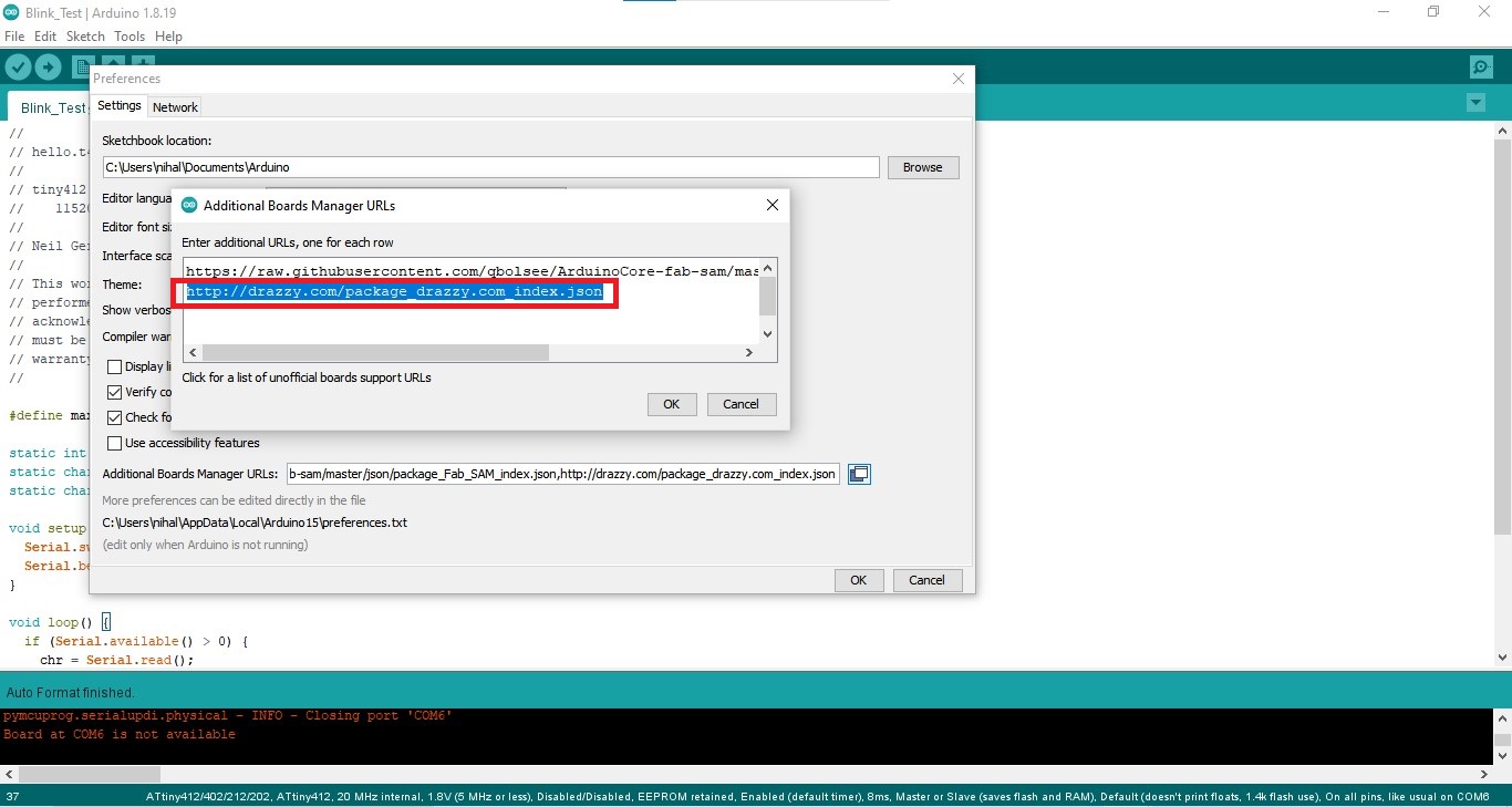
Go to Tool → Board → Board Manager and install MegaTinyCore
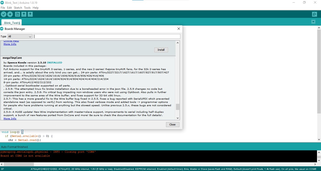
Go to Tool → Port → COMPort
Use the code given on the Fab academy module page(code here )
Click on Upload.
Then my programmer became ready to program.
Then I tested my new board using some Example codes from internet.
int swt = 4;
int led = 0;
void setup()
{
  pinMode(4, INPUT);
  pinMode(0, OUTPUT);
}

void loop()
{

    if(digitalRead(swt) == 1)
    {
      digitalWrite(led, HIGH);
    }
  else{
       digitalWrite(led, LOW);
  }

}
Mistakes I made
- In Fusion 360 Ecad, I made a schematic diagram and I switch to PCB document. I didn’t save the file, and Fusion 360 cracked and I missed my files.
- I delete some components and connections in the schematic and PCB document simultaneously. and I found some wires are missing in the PCB document. Then I synchronize that files.
Group Assignment
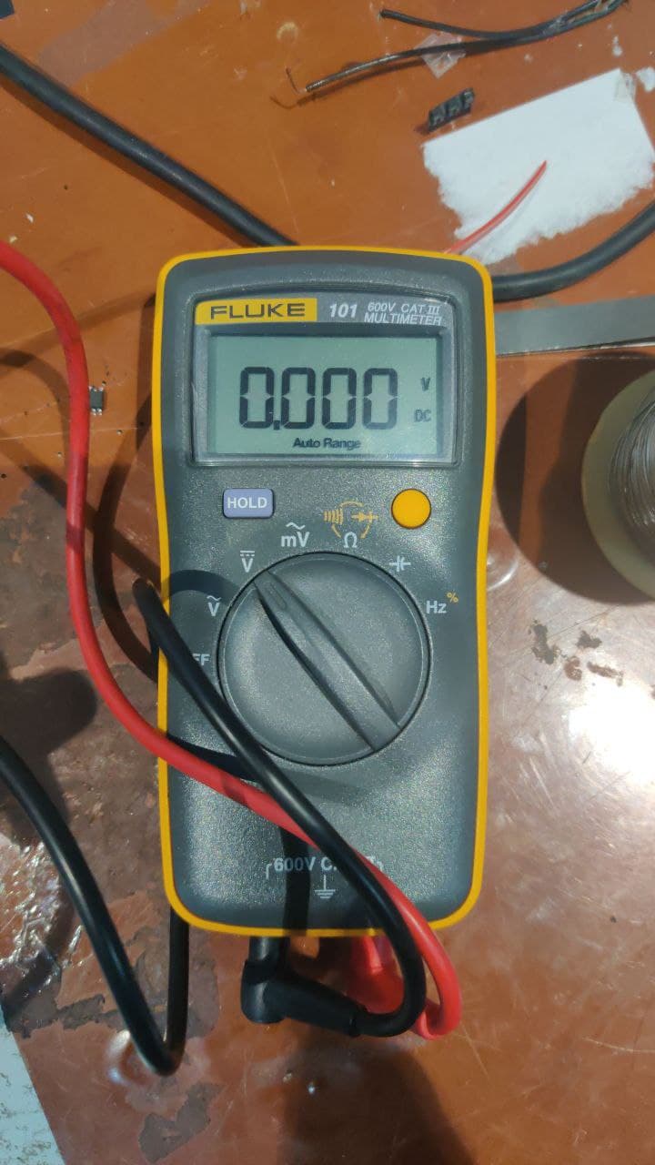
In this week, we learned to use different electronic test equipments.
Testing Equipments
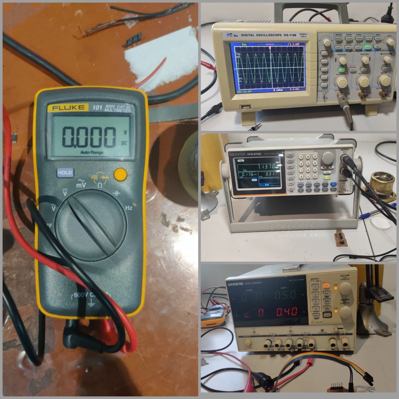
FLUKE 101 Pocket Digital Multimeter
it measures AC/DC voltage, Current, Continuity, Resistance, Frequency, Capacitance
INSTEK GPD-3303D Power Supply
.jpg)
Instek GPD-3303D is a Multiple Output Programmable Linear D.C. Power Supply it have 2/3/4 Independent Isolated Output, LED Display, 1mV/1mA(GPD-2303D/GPD-3303S/GPD-4303S), 100mV/10mA(GPD-3303D) 4 Sets Save/Recall, Tracking Series and Parallel mode, USB Standard Interface, and Lab view driver
INSTEK AFG-2100/2000 SERIES ARBITRARY FUNCTION GENERATOR
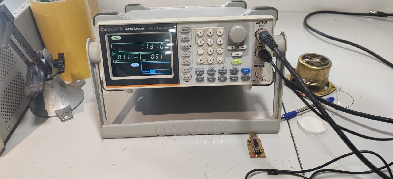
A function generator is a specific form of signal generator that is able to generate waveforms with common shapes. Unlike RF generators and some others that only create sine waves, the function generator is able to create repetitive waveforms with a number of common shapes. The AFG-2100/2000 Series Arbitrary Function Generator is a DDS (Direct Digital Synthesized) based signal generator designed to accommodate the Educational and Basic Industrial requirements for an accurate and affordable signal source covering the output of Sine, Square (Pulse), Ramp (Triangle), Noise and Arbitrary waveforms.it have 0.1Hz to 25MHz with in 0.1Hz Resolution, Sine, Square, Triangular, Noise and, Arbitrary Waveform, 1% ~ 99% adjustable duty cycle for Square Waveform, Waveform Parameter Setting Through Numeric Keypad Entry & Knob Selection, Amplitude, DC Offset and Other Key Setting Information Shown on the 3.5” LCD Screen Simultaneously, AM/FM/FSK Modulation, Sweep, and Frequency Counter Functions (AFG-2100 only), PC Arbitrary Waveform Editing Software
UNISOURCE DS-1100 100 MHZ, 2 CH, Digital Storage Oscilloscope
.jpg)
The digital storage oscilloscope is an instrument which gives the storage of a digital waveform or the digital copy of the waveform. It allows us to store the signal or the waveform in the digital format, and in the digital memory also it allows us to do the digital signal processing techniques over that signal. The maximum frequency measured on the digital signal oscilloscope depends upon two things they are: sampling rate of the scope and the nature of the converter. The traces in DSO are bright, highly defined, and displayed within seconds. it have 100 MHz bandwidth, 1 M Memory, USB storage, RS232C & J45 interface,4000 point record length for each channel,Multi-waveforms math, FFT Function, Cursor & Track measurement, Waveform Record & Recall, Trigger Mode for Edge, Video, Pulse Width, Slope & Alternate
We programmed a board of ATTINY412 with a LED and tested output voltage of output pin using the multimeter and plotted the graph using oscilloscope.
Bill of material
| Part | Value | Device | Package | Description | MANUFACTURER | PACKAGE |
| C1 | 10mf | CAP_UNPOLARIZEDFAB | C1206FAB | |||
| JP1 | CONN_03X2-PINHEAD-SMD | 2X03SMD | PIN HEADER | |||
| R1 | 499 ohm | R1206FAB | R1206FAB | Resistor (US Symbol) | ||
| R2 | 499 ohm | R1206FAB | R1206FAB | Resistor (US Symbol) | ||
| R3 | 499 ohm | R1206FAB | R1206FAB | Resistor (US Symbol) | ||
| S1 | SW_SWITCH_TACTILE_6MM6MM_SWITCH | 6MM_SWITCH | OMRON SWITCH | |||
| U$1 | LEDFAB1206 | LEDFAB1206 | LED1206FAB | LED | ||
| U$2 | CONN_06_FTDI-SMD-HEADER | CONN_06_FTDI-SMD-HEADER | 1X06SMD | |||
| U$3 | LEDFAB1206 | LEDFAB1206 | LED1206FAB | LED | ||
| U1 | ATTINY412-SSFR | ATTINY412-SSFR | SOIC127P600X175-8N | None | Microchip Technology | SOIC127P600X175-8N |