Chemical PCB etching
Cutting the mask
Usually, chemical etching process starts by printing the traces on a transparent sheet, for UV exposure.
As I had no printer (and I wanted to try something new), I cut the traces with a vinyl cutter, directly in the board’s protective sheet.
I used our Silhouette Cameo, with this cutting setup :
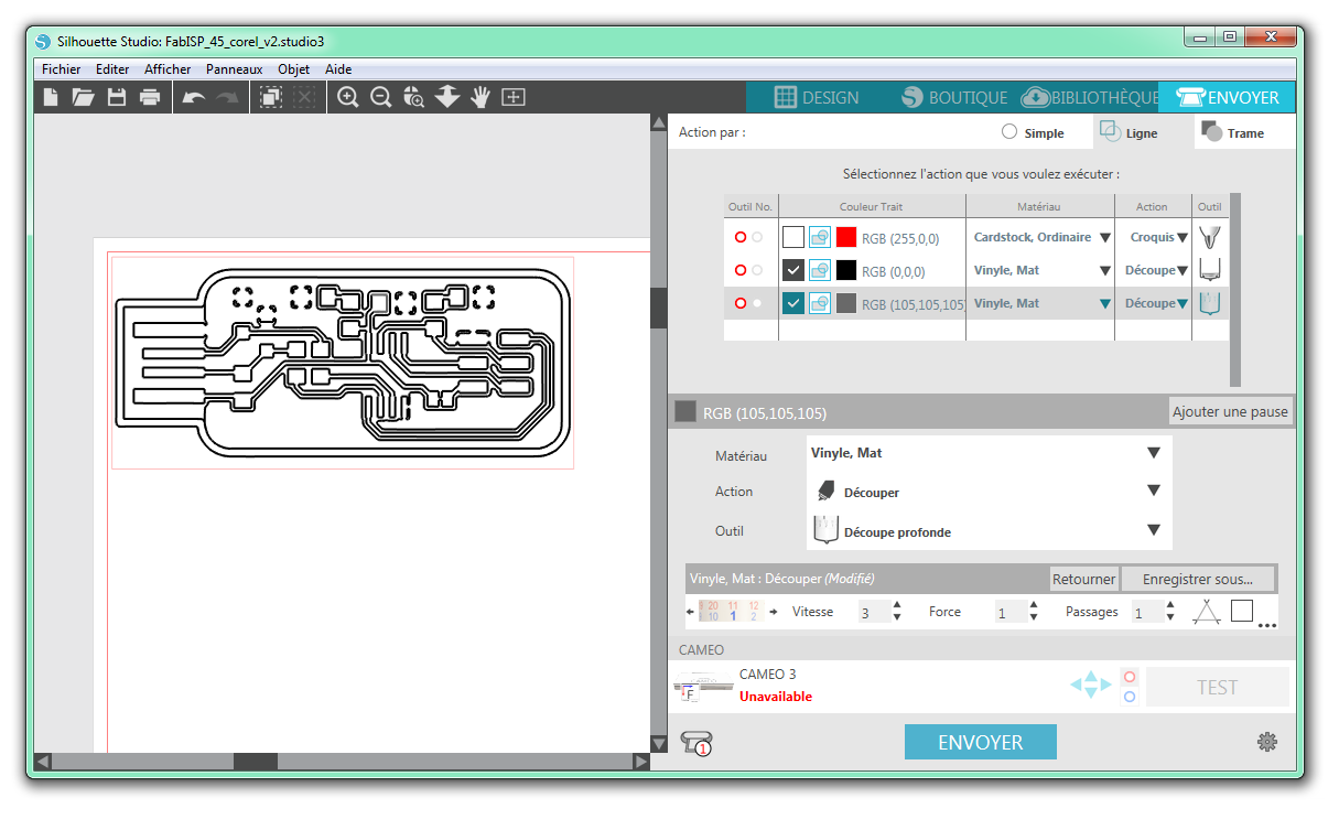
Note that it would be complicated to fit a thick (1.6mm) board in the Silhouette Cameo. So I used a 1mm thick board.
Pelling the isolation traces
Here is the result of the cutting job, and the tools I used for peeling :
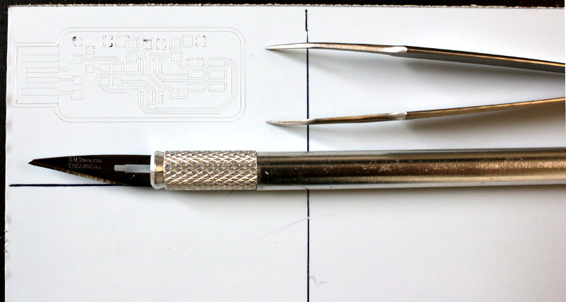
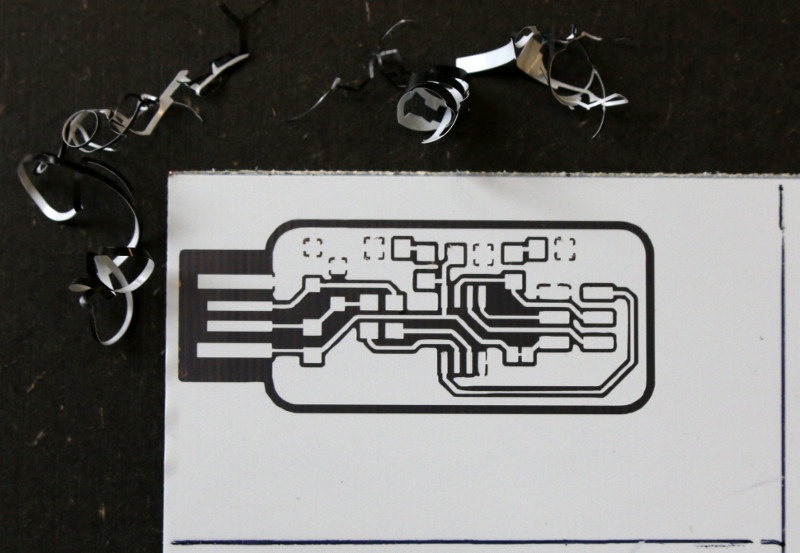
Be careful, because you don’t want to peel pads and tracks ! This is how it looks after peeling :
Cutting the board
Then I cut the board with a shear :
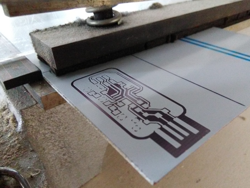
I could not do it before because the board would not fit in the vinyl cutter if it was too small.
UV exposure
For exposure, you need a ultra-violet source. It can be a light bulb, tubes, LEDs or sunlight.
Here, I used a tube lamp from the lab :
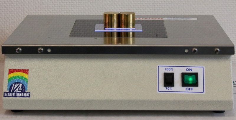
It’s made of six 8W - 312nm tubes and can complete exposure in less than 6min.
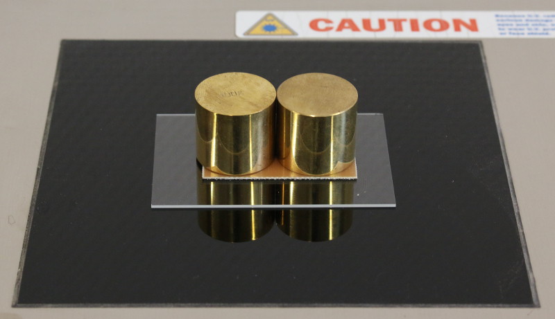
I pressed the board between a thin glass (to keep the window clean) and two 100g weight (to prevent shadows) :
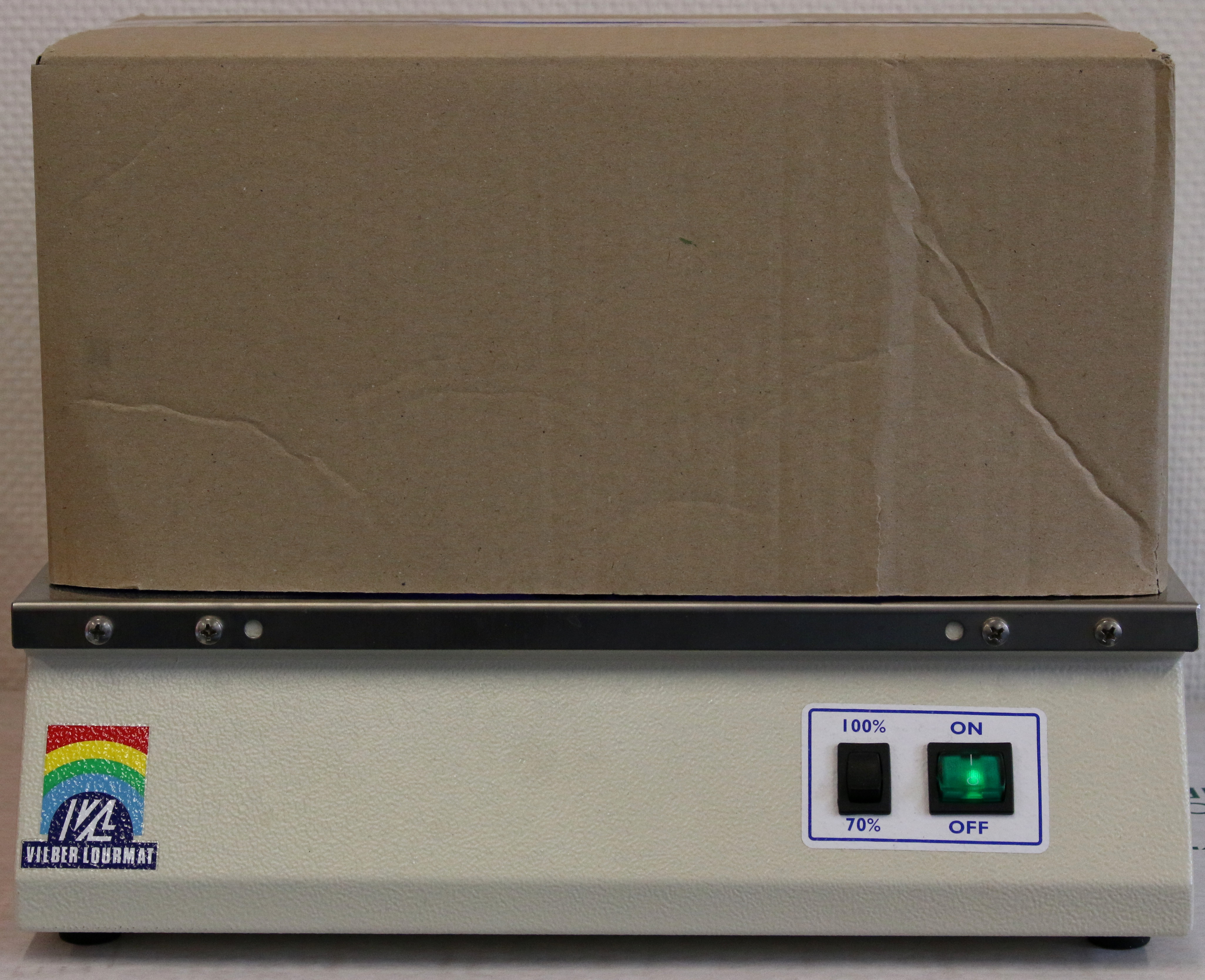
UV light can damage our eyes, so I hide it under a cardboard box :
Cleaning photoresist layer
Now that the board is exposed, you have to remove the photo-resist layer. I dip the board in diluted caustic soda (NaOH) :
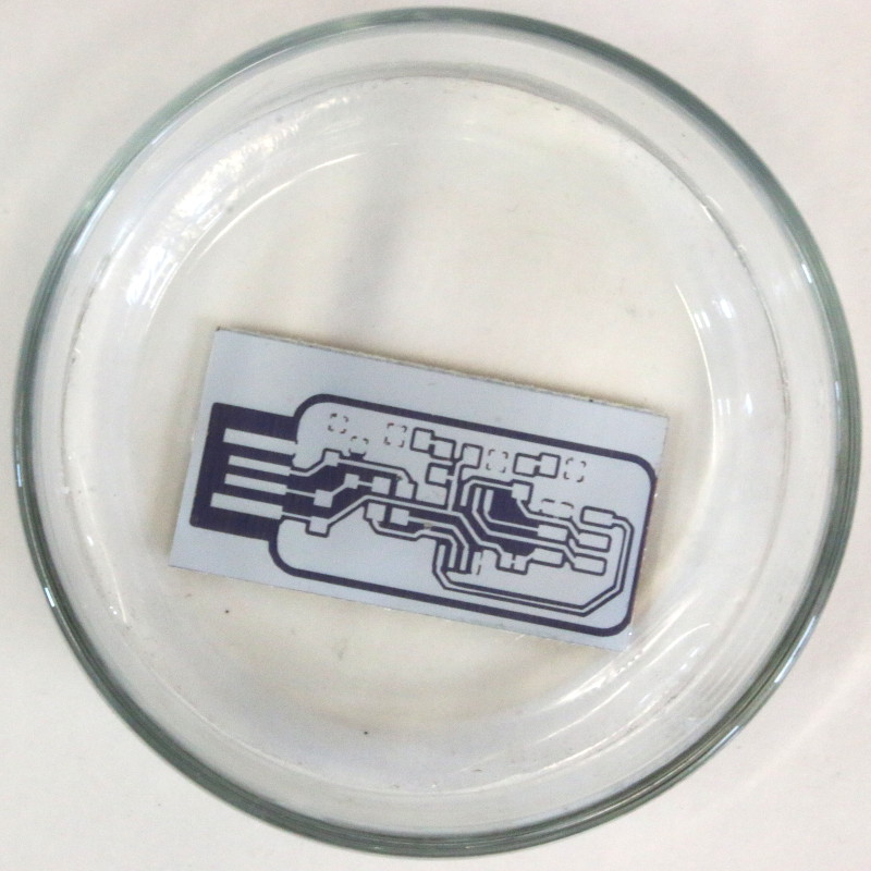
After a while, copper color changes :
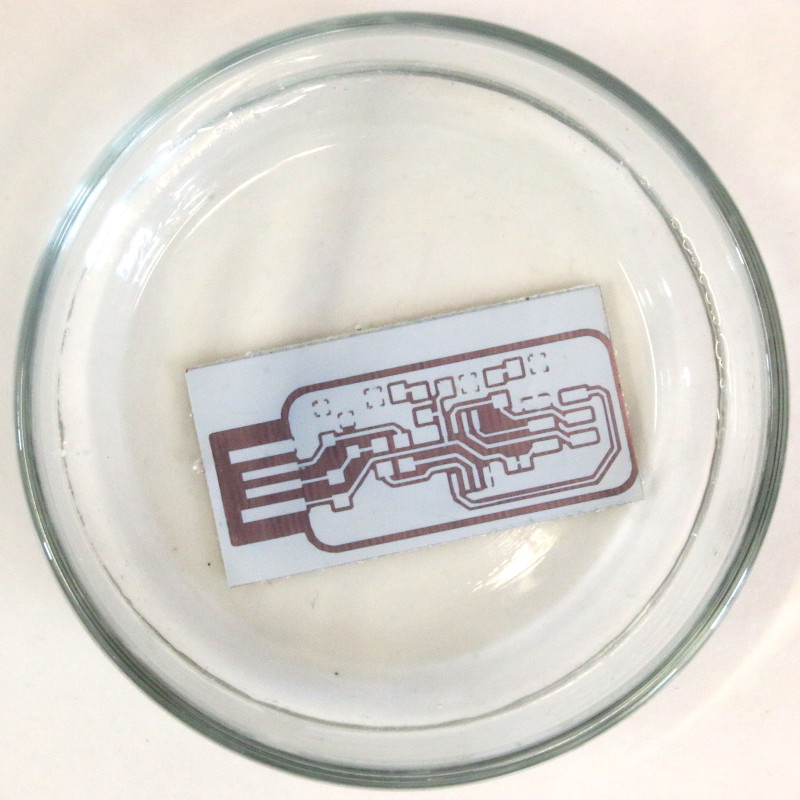
So I remove it using a plastic plier :
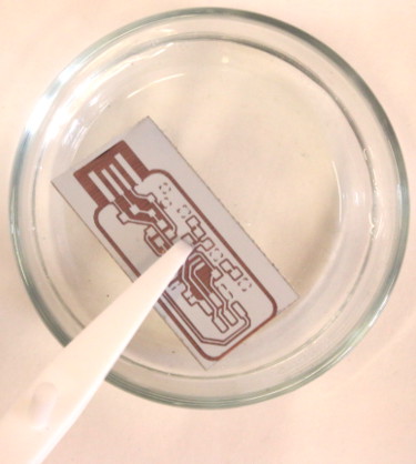
And I clean it with tap water.
Then I remove the mask. If the board is well developed, you can see the traces having a different color :

Etching copper
For etching, I use a solution of sodium persulfate because it’s cleaner than iron perchlorate. Plus, it has the advantage to be transparent (but it gets blue when used, so you can tell it’s efficiency from it’s color).
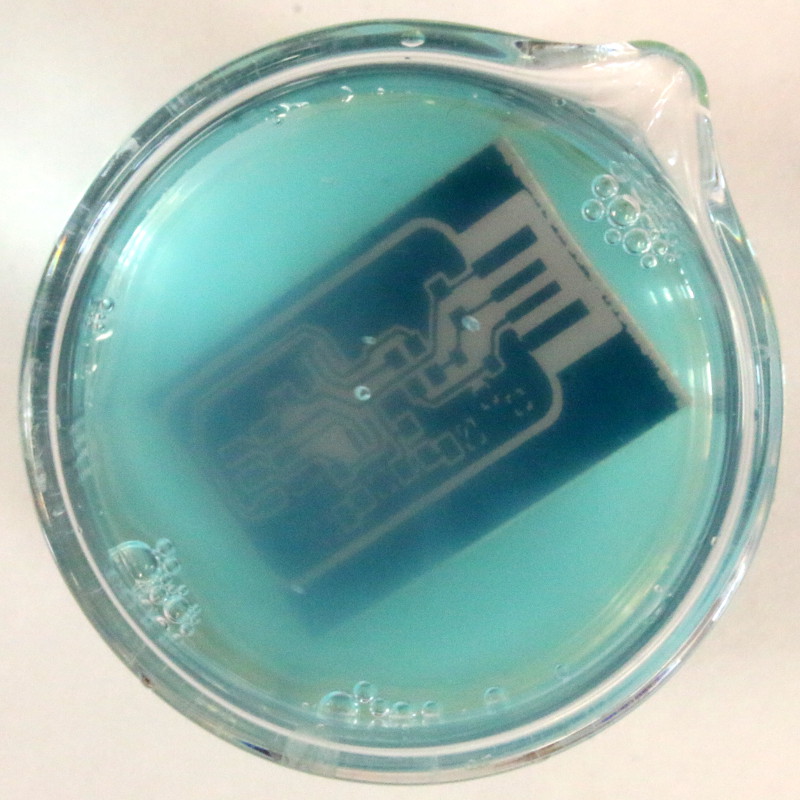
Duration of etching is depends of the temperature of the solution and the saturation in copper salt (a clear solution etches faster than a blue solution). Agitation and air bubbles helps reducing the etching time.
Anyway, you should watch the evolution of etching from times to times if you don’t want to end-up with an over-etched board :
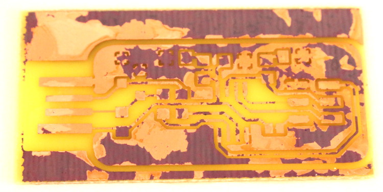
If you see the photo-resist (blue/brown) layer falling of the board, then it is over-etching.
Contour cutting
For cutting the board with the shape of the USB connector, I used a LASER cutter. To make sure that the alignment is correct, I first check it with the red LASER pointer :
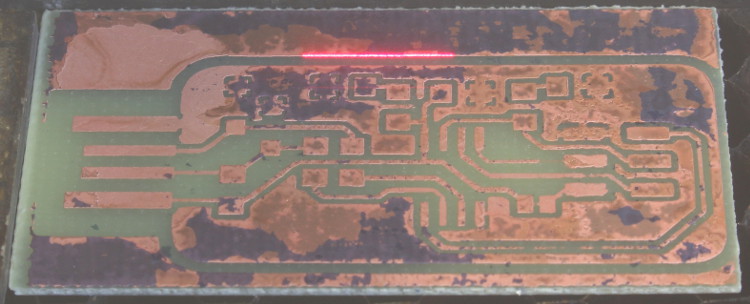
You don’t want to cut into copper because it may damage the optics and the LASER won’t get through.
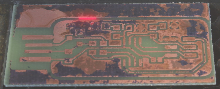
Now the outline drawing is aligned with the PCB, let’s cut it !
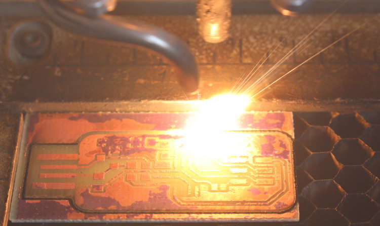
Cutting FR-4 is dirty because it’s blowing fiber glass into flaming dust, so your have to turn on compressed air for the flame suppressor.
Note that it may need many passes to cut through the board. It’s unlikely to achieve a clean cut with a single pass.

Here is the result ! Now you just have to clean out the PCB with water to remove dust.
Before soldering, use acetone to remove the photo-resist layer.