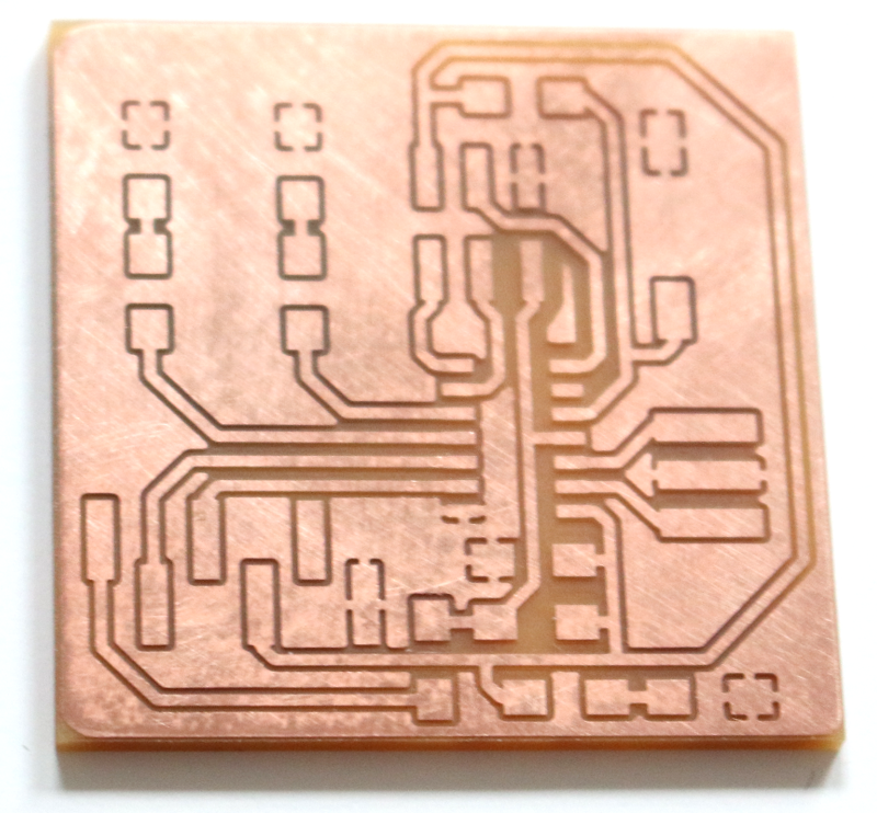
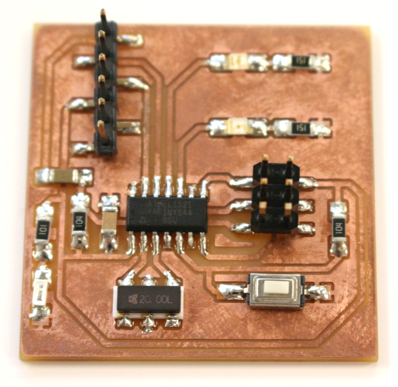
7. Electronics design
Assignment
- Redraw the echo hello-world board, add (at least) a button and LED
- Check the design rules, make it, and test it
- Extra credit: simulate its operation
Group assignment is documented on it’s dedicated page.
Design with EAGLE
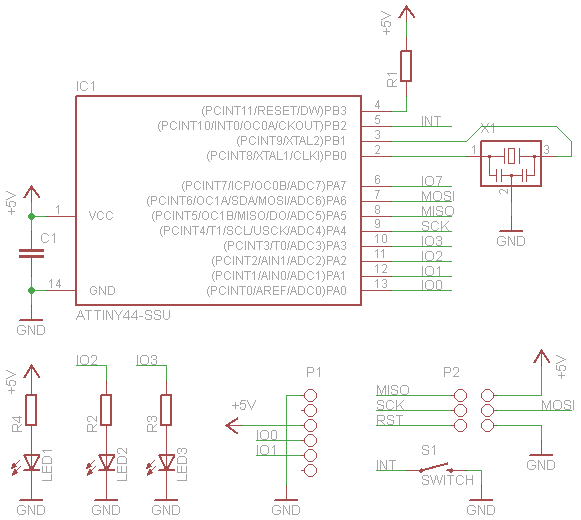
Schematic
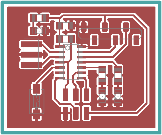
Board
Design rules
I used a clearance of 16mils so I can engrave it with a 0.3mm end mill. BTW, I found out how to export thermal pads to gcode :
- Enlarge thermal isolation in DRC → Supply tab.
- In the pcb-gcode plugin Generation Options tab, set Board Isolation Minimum to less than 0.1mm (I used 0.05mm)
PCB milling
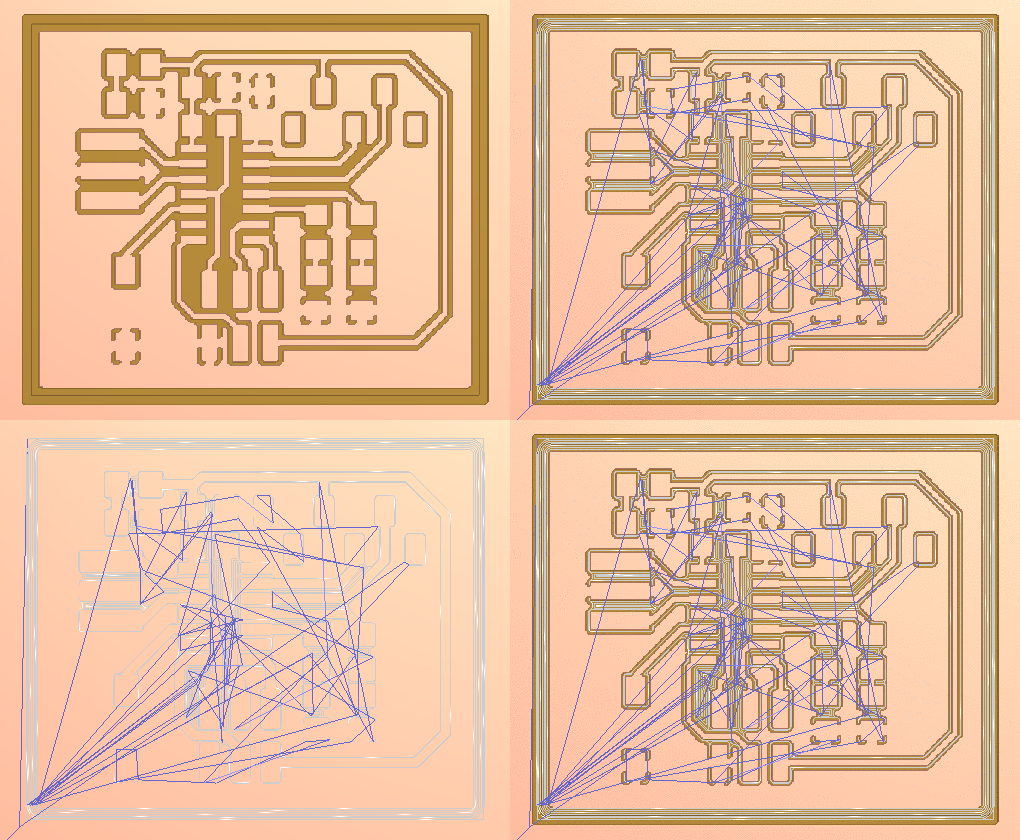
So I exported two g-code files, one for the etching job and another one for the milling job. And this is how it looks in Bantam Tools preview :
Testing with Arduino IDE
Blink test
I first uploaded a simple blink test like the one that I used for the week05 assignment. But this time, I have two LEDs and they are connected to port A :
#define LED1 2
#define LED2 3

void setup(){
  pinMode(LED1, OUTPUT);
  pinMode(LED2, OUTPUT);
}

void loop(){
  digitalWrite(LED1, HIGH);
  digitalWrite(LED2, LOW);
  delay(500);
  digitalWrite(LED1, LOW);
  digitalWrite(LED2, HIGH);
  delay(500);
}
I selected ATtiny84 (external 20MHz clock) in Tools → Board but after uploading the sketch, LEDs were blinking very slowly. I had to use Tools → Burn Bootloader to tell the ATtiny84 to use its external clock. And then, upload the sketch again.
Push-button test
This code is supposed to switch the LEDs when the button is pushed :
#define LED1 2
#define LED2 3
#define BUTTON 8

void setup()
{
  pinMode(LED1, OUTPUT);
  pinMode(LED2, OUTPUT);
  pinMode(BUTTON, INPUT_PULLUP);

  digitalWrite(LED1, HIGH);
  digitalWrite(LED2, LOW);
}

void loop()
{
  if(!digitalRead(BUTTON)){
    digitalWrite(LED1, !digitalRead(LED1));
    digitalWrite(LED2, !digitalRead(LED2));
    delay(200);
  }
}
Software Serial test
I uploaded this code to test serial communication :
#include <SoftwareSerial.h>

#define RX 0
#define TX 1
#define LED 2
#define BUTTON 8

SoftwareSerial mySerial(RX, TX);

void setup()
{
  pinMode(LED, OUTPUT);
  digitalWrite(LED, LOW);
  pinMode(BUTTON, INPUT_PULLUP);
  mySerial.begin(9600);
  mySerial.println("Hello world");
}

void loop()
{
  if(mySerial.available()){
    digitalWrite(LED, HIGH);
    delay(100);
    digitalWrite(LED, LOW);
    delay(100);
    mySerial.flush();
  }
  if(!digitalRead(BUTTON)){
    mySerial.println("Push !");
    delay(200);
  }
}
It works as expected, but I can’t see the Hello world in the serial monitor because it is send at power-up.
If I want to see it when I open serial communication, reset pin must be connected to the FTDI’s DTR pin.
ATtiny pins names
When I first tried to test the push-button, it did not worked. The µcontroller was reading it LOW, no matter if it was pushed or nor. I thought this was because it needed an external pull-up resistor.
In fact, the internal pull-up resistor did the job. The reading issue was because I named the input pin PB2, according to the datasheet. But Arduino IDE did not interpreted it correctly, so I had to refer to it using the number 8 (this is defined in hardware\attiny\variants\tiny14\pins_arduino.h).
To avoid making the same mistake, always use Arduino pins numbers. The brown ones in this diagram :

By the way, I recommend you to download this ATtiny pinout diagram.
Design with KiCAD
Schematic
I improved my first EAGLE design with a pull-up resistor for the push-button and a capacitor connecting the reset pin to the FTDI header.

Once you are done with the schematic, click on the Annotate schematic components button to give a reference number to each component :

just click on the Annotate button and it will be done automatically.
Footprint association
Now, click on the Run CvPcb button to begin footprint association :

Here there are 3 filter buttons that helps you find the proper footprint :

- The first one uses keywords (not very reliable).
- The second one uses pin count (useful, but not necessary).
- The third one uses the library you selected in the left frame.
The filtered footprint list is displayed on the right frame. To see how the selected footprint looks like, click the View selected footprint button :

Double-click on the footprint’s name to associate it with the selected component (in the centre frame).
When you are done with the association, click on the Save button :

Board design
Prior to begin the PCB design, click on Generate netlist :

And click on the Generate button. It’s all you need to start the PCB design so click on Run Pcbnew :

To move a component, right-click on it. If the selected part needs clarification, you will have to click on the corresponding footprint. Then select Move.
Before drawing tracks, it can be useful to define the isolation clearance with the DRC :

To create a track between two components, use the Add tracks button :

To draw a copper plane, use the Add filled zones button :

When the copper plane shape is drawn, you have to right-click on the contour line and go to Zones → Fill Zone to see the result.
Footprint edition
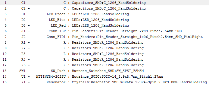
All the footprints I needed were included in the standard libraries of KiCAD.
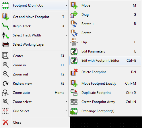
But some pads were too shorts, so I had to edit footprints. So I right-click on the footprint and select Edit with Footprint Editor :
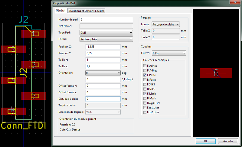
In the editor, you can edit the size and position of a pad with a right-click on the pad → Edit Pad.
When edited, footprint have to be saved in a new library (I named it HelloBoard.pretty). Then you have to add the new library to your project, using Preferences → Footprint Libraries Wizard. The new library will be included in your project :
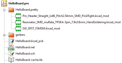
To replace footprints in your PCB design, right-click on part and select Exchange Footprint then View Footprints and choose it in your new library.
Finished PCB drawing
Here is my new PCB design :
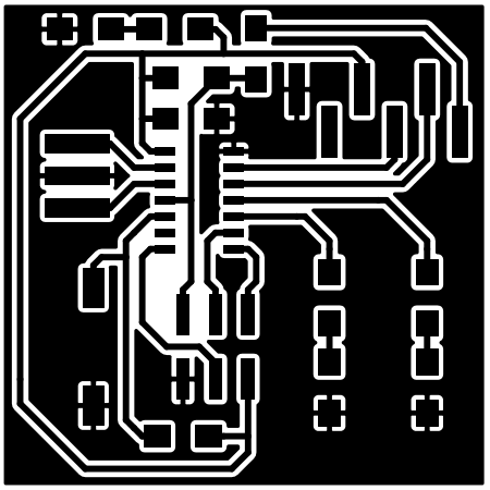
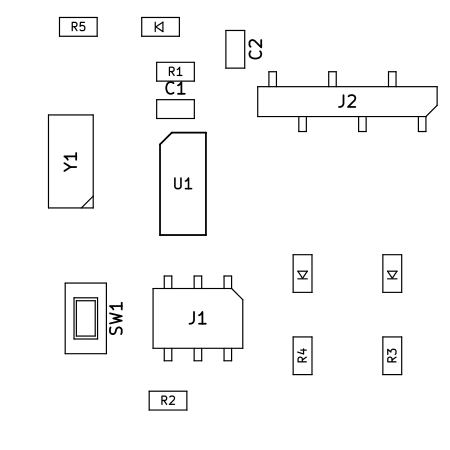
Gerber output and milling
To create a gerber file that is compatible with the Bantam Tools milling machine, I followed these instructions.
There are advantages to use gerber instead of gcode, with the Bantam Tools milling machine :
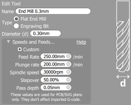
- You can change pass depth, stepover, and speeds (in the Tool Library).
- You can choose trace depth (in the Advanced section).
- You can change the trace clearance and see the preview directly.
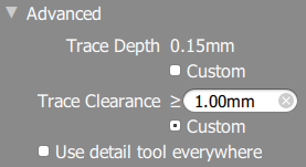
I used these parameters for etching traces :
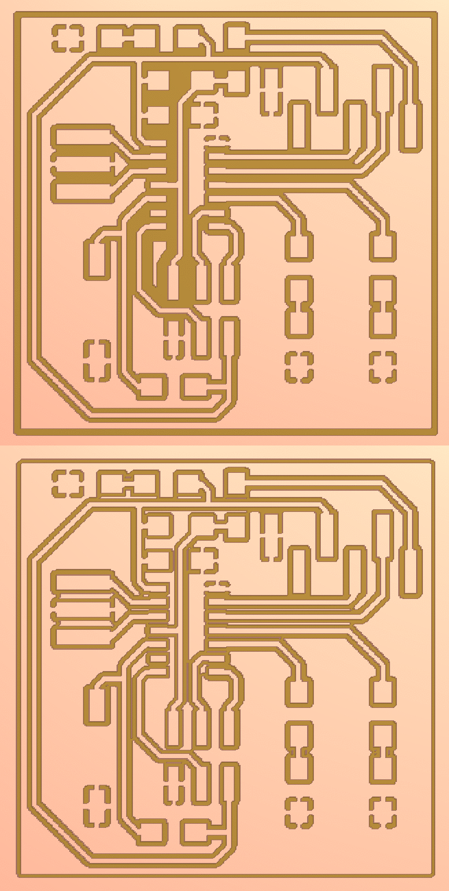
As you can see in this animation, trace clearance does not affect the ground plane isolation (that you have to define in KiCad’s DRC) but it helps to remove copper between traces :
Soldering components
