Electronics Design
Week 06
5th-12th March 2014
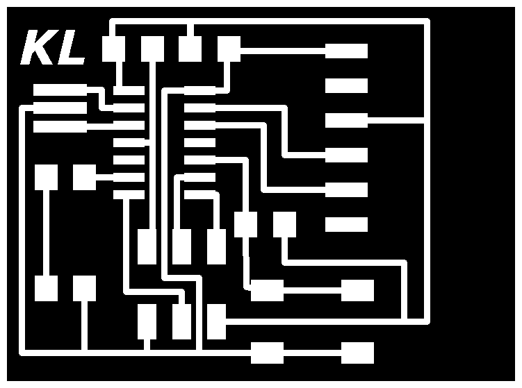
After practicing milling and surface-mount soldering two weeks before, this week's assignment was to (re)design a PCB using and manufacture it in the lab. As usual there were a whole lot of options provided from the class to be explored. The obvious choice for desigining a PCB seemed the industry standard Eagle package. It's freeware edition is limited to single-layer boards only, therefore I decided to give a shot at the KiCAD package first. After doing a couple of tutorials there, fellow student pointed me to the AS220 Eagle tutorial and indeed it worked like a charm. Very detailed and accurate walk-through of Eagle resulted in a decently designed and milled board within an hour.
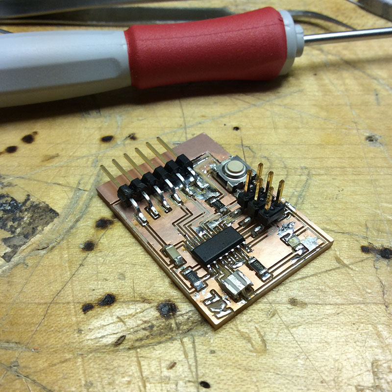
Milling the board was pretty straightforward with the FabModules, however the only problem was that Modela's table was not exaclty parallel to the coordinates of the spindle. Result - half-milled board. To make sure that the next attempt delivers result - I pushed the bit quite a bit deeper. It seemed to work this time, bu need to find a better solution for the next project. Populating the board was a bit of an adventure (somehow it was trickier than it was with FabISP), but an hour of patient work and the board was there. Not as clean as I hoped it to be, but looks ok nevertheless. Will be testing it in two weeks - fingers crossed until then.
design files can be downloaded here:
