7. Electronics design
1. Weekly Brief Summary
Using Eagle, they designed electronic circuits and boards, and built a base with buttons and LEDs to verify their functionalit
2. Weekly Assignment Requirement
-
Group assignment:
- Use the test equipment in your lab to observe the operation of a microcontroller circuit board (in minimum, check operating voltage on the board with multimeter or voltmeter and use oscilloscope to check noise of operating voltage and interpret a data signal)
- Document your work (in a group or individually)
-
Individual assignment:
- Redraw one of the echo hello-world boards or something equivalent, add (at least) a button and LED (with current-limiting resistor) or equivalent input and output, check the design rules, make it, test it.
3. Group Assignment
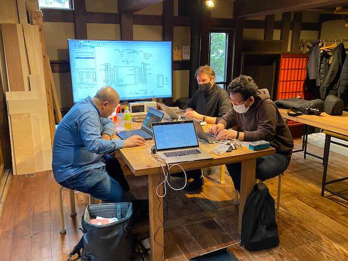
FabLab KAMAKURA 2021 Lab site / Electronics design
4. Electronics design with Eagle
For the design of the electronic circuits, I used Eagle , which has a free version that can be used for free with certain restrictions.
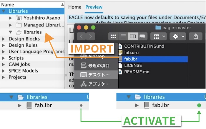
Add library
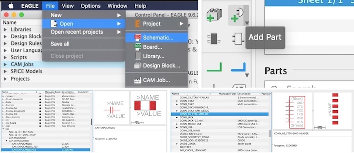
EAGLE is software that allows you to create a schematic by placing electronic parts. You can design the original electronic parts yourself, but it is more convenient to use an existing data set (library). This time, I used the one prepared for FabAcademy and the one from Atmel to make up for the shortage.
Unzip the required data and drag and drop the “lbr” file inside to the “ibraries” folder in the Eagle Control Panel. You cannot use the file as it is, so click on the gray dot to activate it and change it to a green circle.
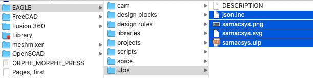
SamacSys PCB Library
Use the “amacSys plugin” as a more comprehensive and easy to handle library.
SamacSys / EAGLE Library Plugin
【1】Click Download on the web page to download the zip file.
【2】Unzip the file and open Mac OS and Linux.
【3】Copy samacsys.svg,samacsys.png, json.inc and samacsys.ulp to .../documetns/EAGLE/ulps/.... NOTE:ulp stands for User Language Program
【4】Open Eagle Control panel , select File > Open > Script > eagle.scr.
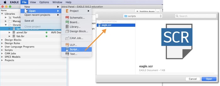
【5】Update ① & ② as '[users/USERNAME/documents/EAGLE/ulps/samacsys.svg] SamacSys : Run samacsys.ulp;'\
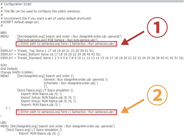
CAUTION :Don’t confuse `(backquote) with ‘(single quate).
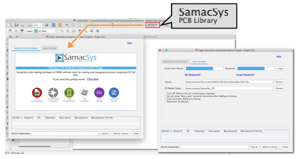
【6】 Open new project, click SamacSys logo.
【7】Sing up as Autodesk user and sign in.
【8】Make new library for SamacSys like SamacSys_Parts.lbr for example, and add write it on Settings.
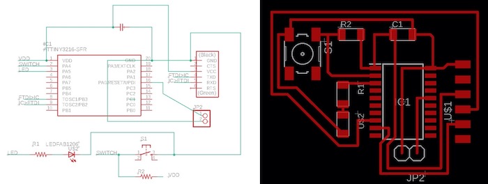
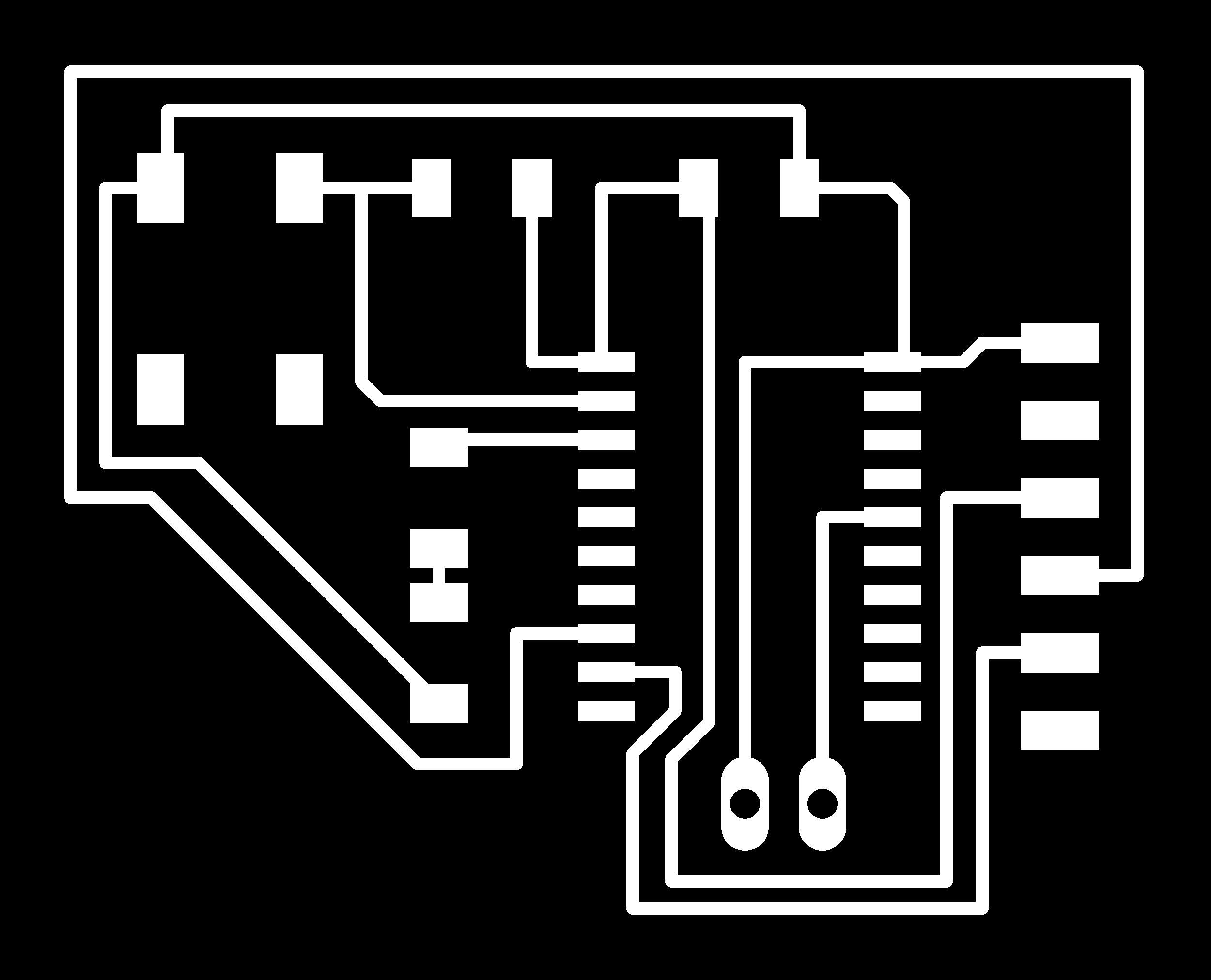
Schematic
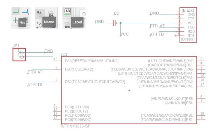
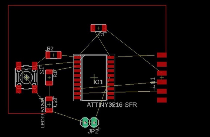
Open schematic board, and add electronics parts from library. Net can wire part to part, Label can add label. Name enable name wires and shortcut. Connect the parts in the correct order, comparing them with the completed drawing.
Board
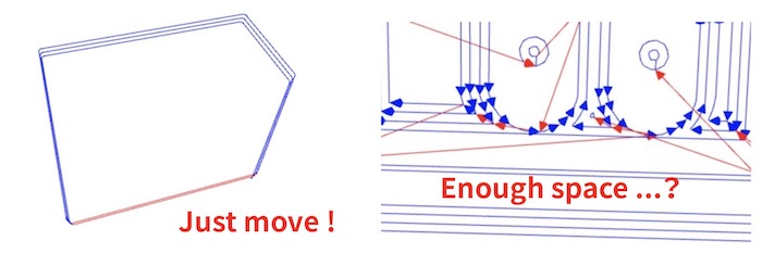
Once the schematic is completed to some extent, move on to the board design. The parts that are connected to each other are connected by yellow battles, so we can draw lines based on these lines.
TIPS:If there are multiple ways to connect, the yellow line connects the one with the shortest distance.
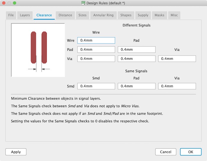
Move to Edit > Design Rule > Clearance , the distance between parts and wires can be specified. The default setting is too thin, so I set all the values to 0.4 mm this time.
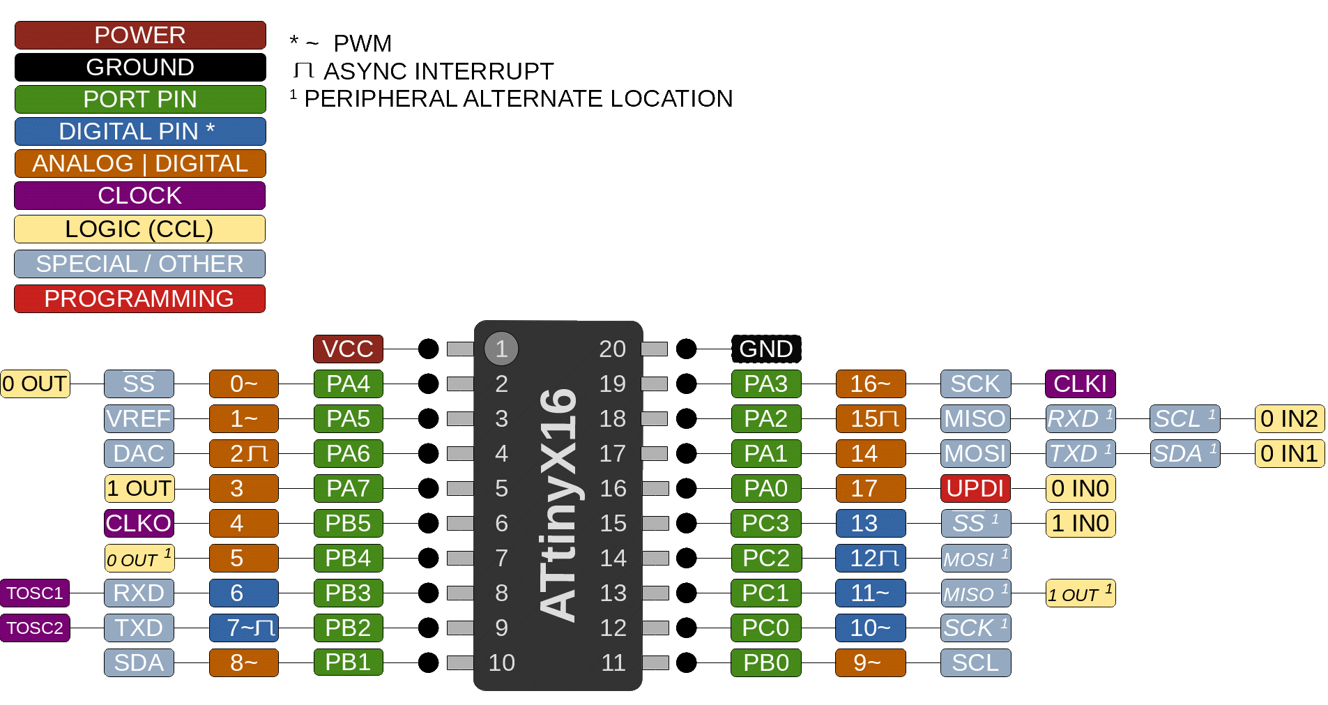
Autorouting will automatically route the wires for you, but it is not very efficient, or there may be a glitch somewhere. It is best to design the board while using it as a reference only. I Used the pin layout of the ATtiny3216 as a reference, I completed the wiring, taking into account the behavior of the switches and LEDs.
Export Process file
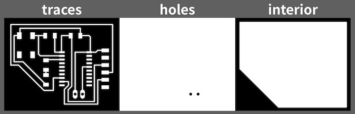
After making board image, I have to make 3 process files, traces, holes and interior. Let’s make them with using layer function on Eagle.
traces
Layers > Used Layers, select Top and Pads.
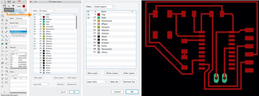
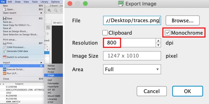
File > Export > Image, and must check monochrome, set the resolution to 800 dpi . This settings are same for other parts.
holes
Export Pads only monochrome png file, and have to edit it as below.

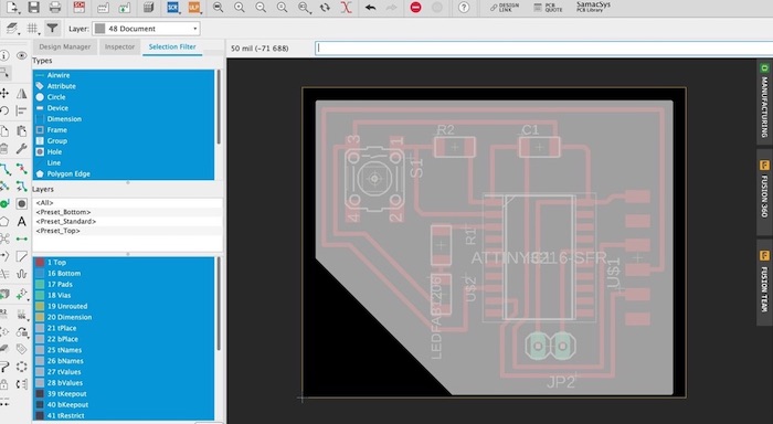
interior
When make interior, use 48 Document layer. Polygon tool is easy and comfortable to boards’s external. Also check and edit 20 Dimension layer to control total size of board.
5. Fix Data / Milling and Soldering
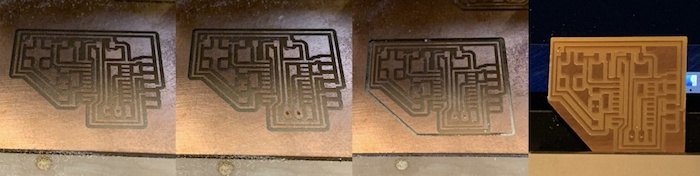
Use mods to make .rml file as assignment of electronics production. I summrize path-making flow as below.
- Access to mods.
- Right Click > program > open server program → SRM-20 / PCB-PNG
- Read png > click「select png files」to load board image.
Roland SRM-20 milling machine> Origin x, y, z → 0mm- Right click > modules > open server module > Add save node.
- Connect outputs’ file to inputs’ file(objects) by click each node.
- Set PCB defaults - select mill traces(1/64) for trace, mill outline(1/32) to interior.
- Mill raster 2D - click calculate to make .rml file. Parameters are changed automatically by select mill traces(1/64) or mill outline(1/32).
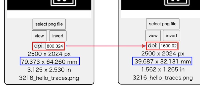
If you use Mac Retina-Display machine, have to double the resolution number. The size of the finished board will also change, so make sure it is correct.
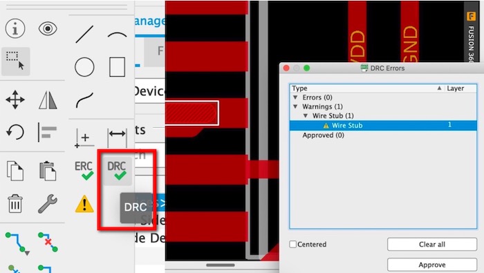
Check .rml simulation, and found some erros or mistakes. Too narrow space to cut, not enough gap to solder, etc.
For correcting errors on Eagle, DRC(Design Rule Checking) is useful.
Finally, I got theese 3 png and .rml files and process it on SRM-20.
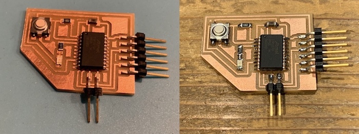
| Parts Name | Quantity |
|---|---|
| ATtiny3216 | 1 |
| 1uF Capasitor | 1 |
| 6 pin connector/FTDI | 1 |
| 2 pin conncetor/UPDI | 1 |
| Tact switch | 1 |
| 10kΩ Resistor | 1 |
| LED | 1 |
| 511Ω Resistor | 1 |
After cutting out, let’s solder it. The previous FX302 was too difficult, so this one felt much easier.
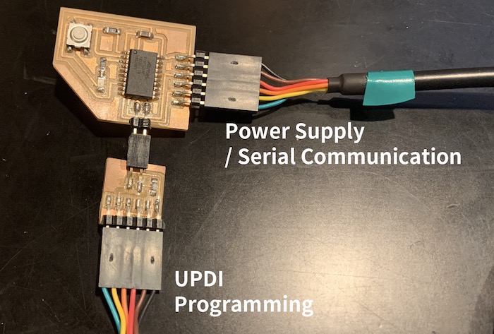
6. Function Check
For programming, UPDI connection and Power supply are also needed.
hello.t3216.echo.ino
Button & LED
void setup() {
  pinMode(1, OUTPUT);
  pinMode(2, INPUT);
}

void loop() {
  if(2 == HIGH){
    digitalWrite(1,HIGH);
  }else{
    digitalWrite(1,LOW);
  }
}
7. Links to Files and Code
Files
- EAGLE schematic,helloATtiny3216.sch
-
EAGLE board, helloATtiny3216.brd
- png_02_3216_hello_holes_invert.png
- png_03_3216_hello_interior.png
- mill_01_3216_hello_traces.rml
- mill_02_3216_hello_holes.rml
- mill_03_3216_hello_interior.rml
Links