- Characterize the design rules for your PCB production process
- Make an in-circuit programmer by milling and stuffing the PCB
- Test it, then optionally try other PCB processes
Group Assignment
Individual assignment
Learning outcome
- To understand the PCB milling machine
- To get more familier with SMD componants and test it
- Hand's on soldering iron & Hot air gun
- To understand the Software installation part specially on Linux platform
- Test the my FABISP
Table of Content
- ROLE of MOD
- SRM 20 for PCB Milling Machine
- Stuffing & Soldering
- Build Programmer
- PCB miling video
- Update1
- Update2
- Update3
- Downloads
Hero Shot
Group Assignment
The task of the week is to Characterize the design rules for your PCB production process.As a part of group assignment i worked on fab mod and try to figure out following things and then later on we all go to finalised design rules.
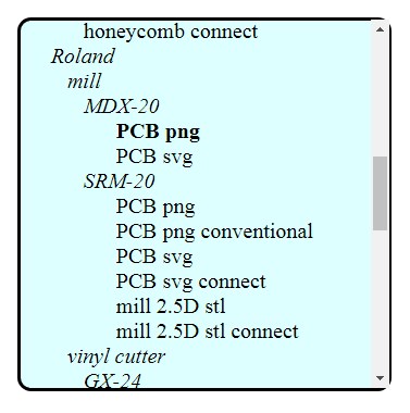
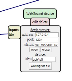
How to use the online MODS to make files to mill your own circuit boards!
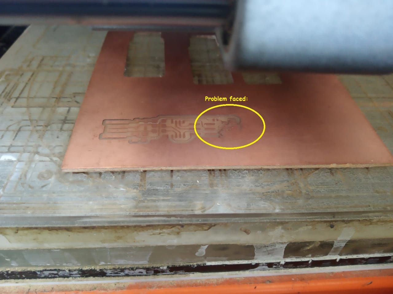
While discussing with our instructor i came to know that if the sacrificial layer is uneven then your SRM-20 will not milled the board.So he asked me to study more about the cut depth and i analysed the some points.
Group Assignment
Individual assignments on PCB milling machine
Introduction
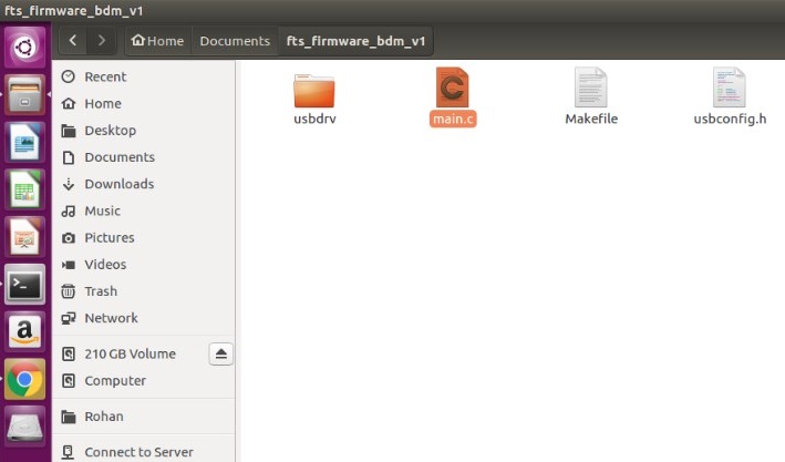
As we know this week is all about Electronics production.In this week we have to milled the given design of Fab ISP.So to do this we need to folloew some procedure like generating rml file ,milling using SRM-20 machine and then fixing and soldering og componant etc...
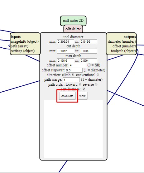
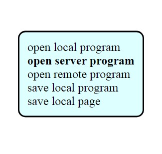
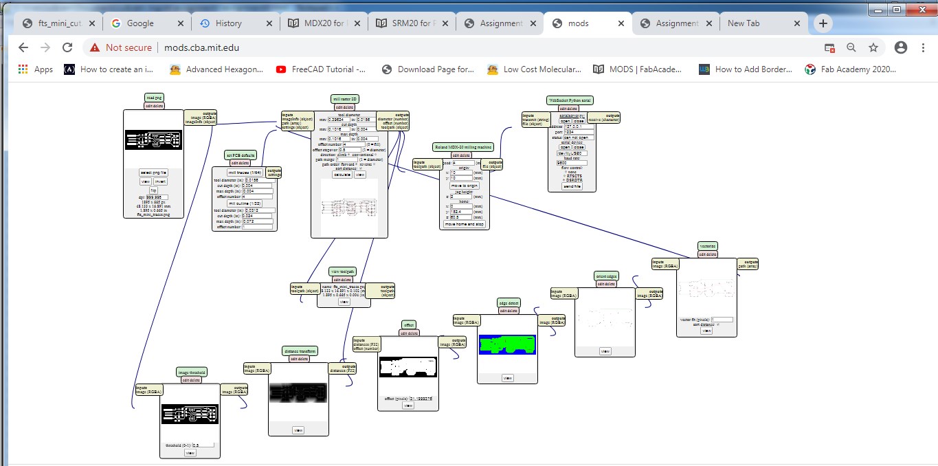
Step 1.Role of Mod software for generating png to rml file
Why we need rml file?
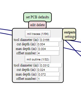
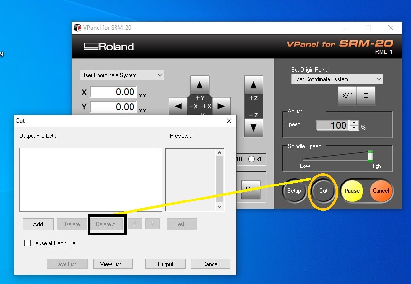
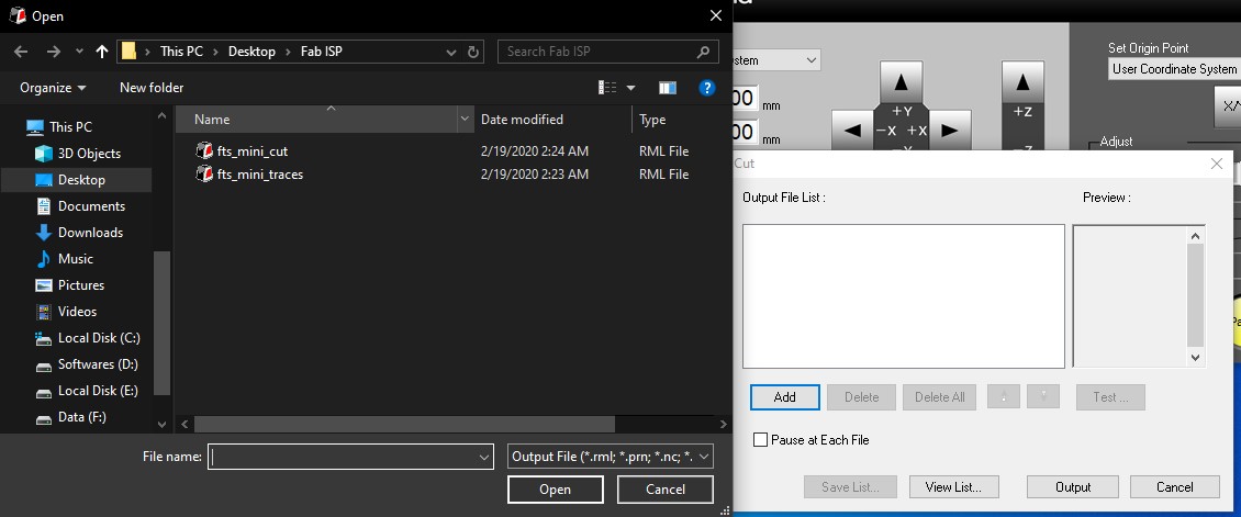
For milling my FABISP i am going to used SRM-20 PCB milling machine.This machine required traces,hole drill and outline rml file.
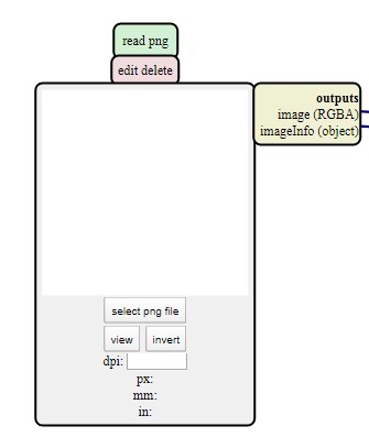
We have FABISP png file which i am going to convert into rml using MOD software.MODS is the new FABMODULES which is capable and works by connecting nodes to develop each process.Using this i am going to generate the traces and outline file.Following procedure gives you an step by step idea of it.
- Read PNG module > Select PNG file of my PCB design
Similarly,use the same procedure for outline files as well.
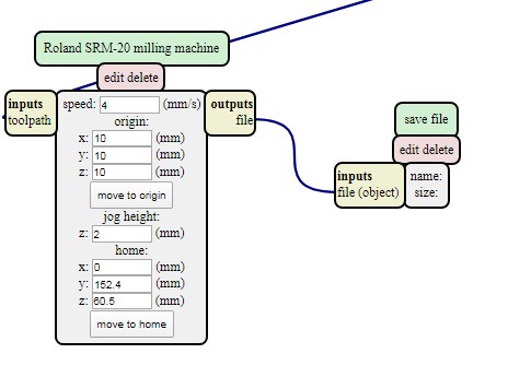
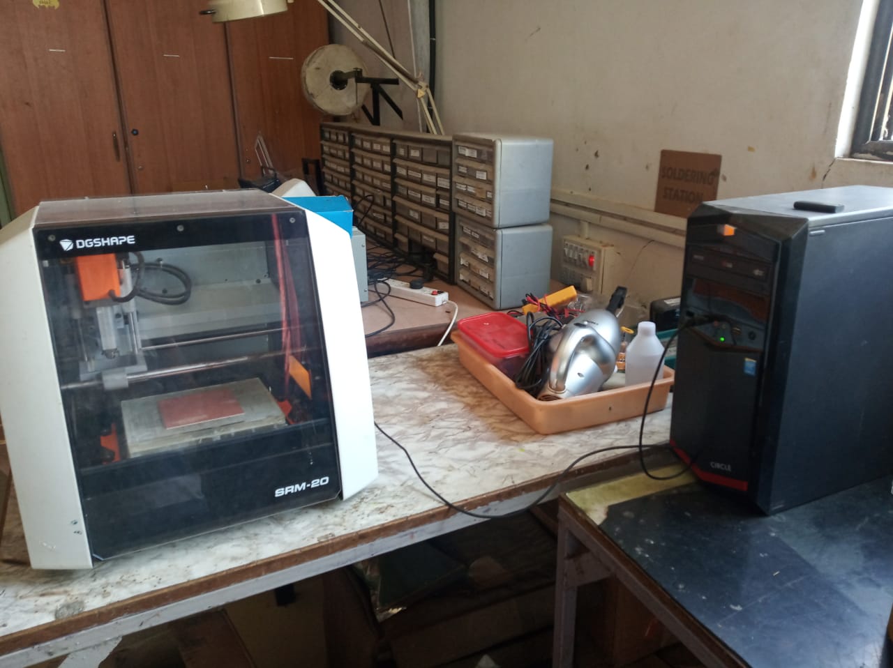
Step 2.SRM 20 for PCB milling machine
Once we are ready with trace and outline file in rml using MOD then we need to go for PCB milling.For PCB milling we need to first explore the SRM-20 machine.
About SRM-20
Introduction:The SRM 20 is a Roland 3D next generation desktop milling machine for the office,studio and education environment.The SRM 20 incoprparate innovative features including a new spindle,collet,circuits boards and control softwares.
The SRM -20 can mill variety of material typicaly used for prototyping,including chemial wood ,acrylic and modeling wax.
Understanding SRM-20 other than PCB milling
Making of sacrificial layer using SRM-20
Miling wax to crate a mold using SRM-20
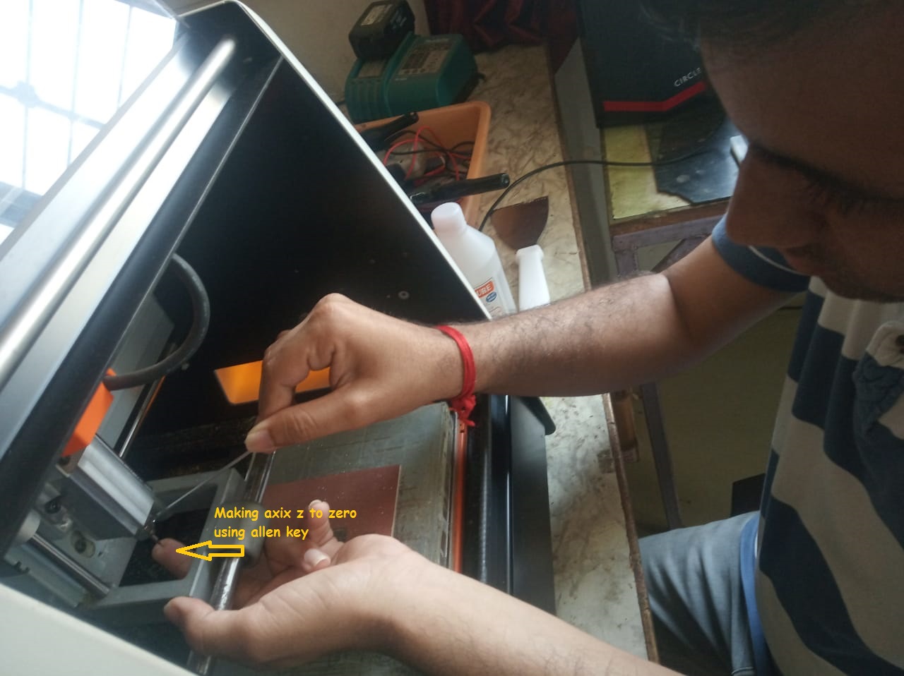
Exploaring SRM -20 for my PCB milling
Step 1
Features :Design for clean and secure use in your office or classroom
The SRM-20 include an interlocked full cover and dust collection tray to keep your envirnonment clean and clear waste material.For increased safety opening cover automatically stps the machine.Above information taken from Roland SRM-20 official page
Step 2
Features:Simple operation for optimum results
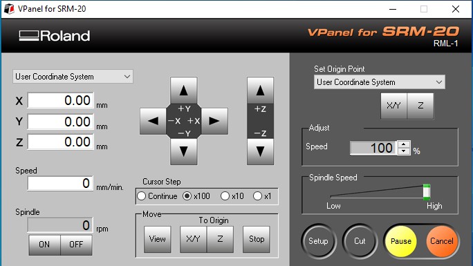
Design for easy to use ,the SRM -20 supports Roland DG'S unique "VPanel" an on-screen operation panel for the computer.By using the speed-controlled 4-way cursor movement,the origin point can be set quickly and accurately.Spindle RPM and milling speed can be altered during milling ,allowing full control over the resuls and milling time.
The SRM-20’s VPanel controller provides a simple interface for adjusting tool position and moving the cursor to set the milling starting point. The VPanel also allows easy control of feed rate and spindle speed with pause and resume operation, plus tracking of X,Y,Z axis milling with a numeric readout in millimeters or inches.Above information taken from Roland SRM-20 official page
Once i did all these things our SRM-20 Machine gets started.I really enjoyed the sound of the machine.
See this is what happened!
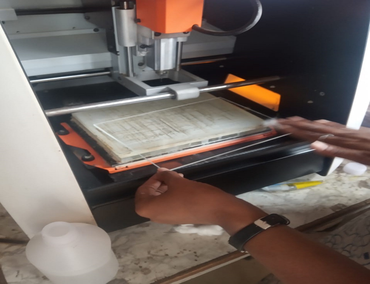
Change the Sacrificial Surface
.
PCB miling video:
PCB milling Machine video
See this is what happened!
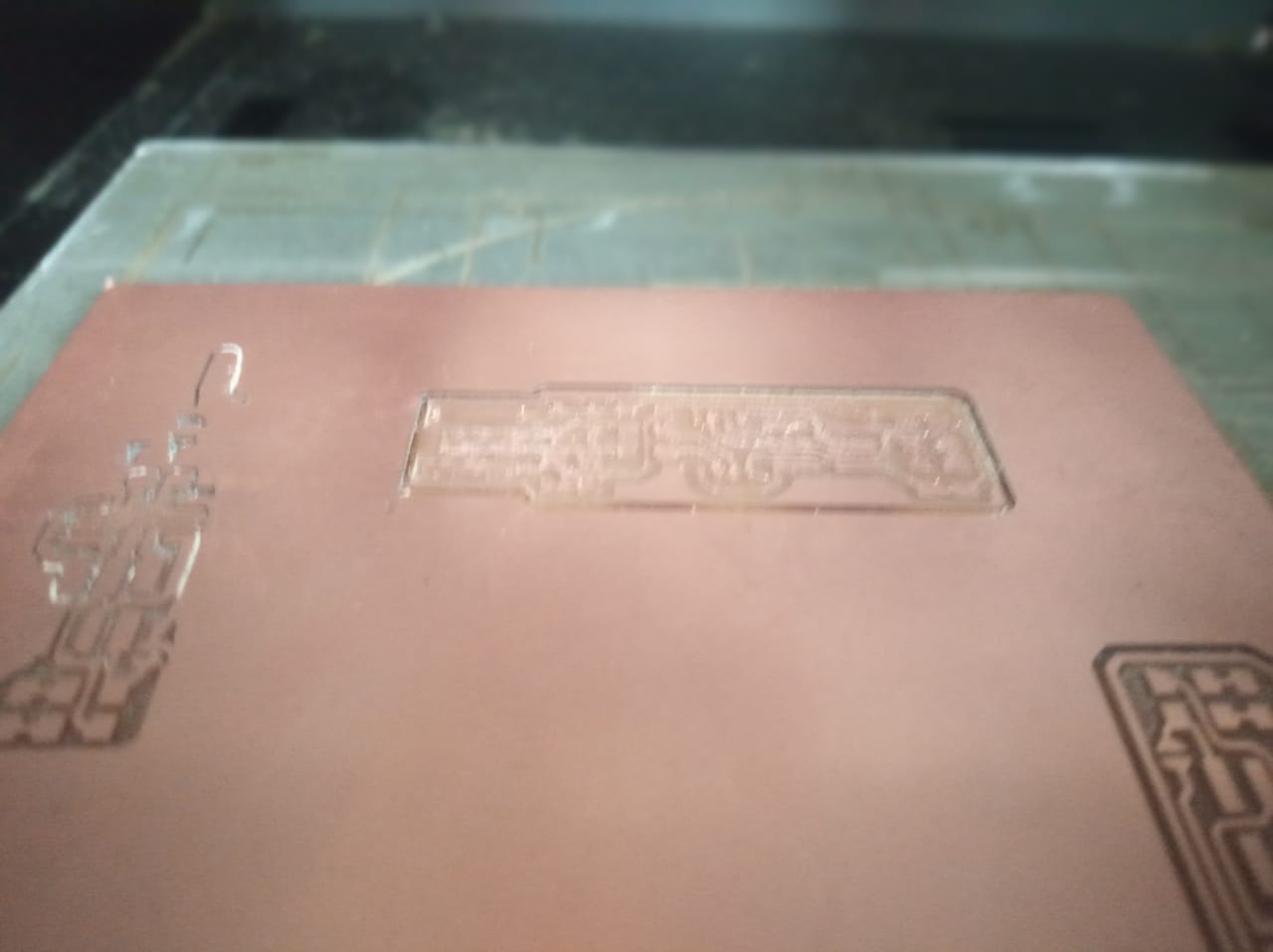
Now its perfectly fine
Then i removed the PCB from surface board smootly using spatula.
Point to be noted:The reason behind not milling the PCB properly is that the yoursacrificialsurface is not flat.Also there was a some material(glue of two sided tape) left behind onsacrificialsurface so what we need remember is that please remove material from the surface and make it clean.
Step 3.Stuffing & Soldering
"Soldering is all about uniting the two things of metal called solder."
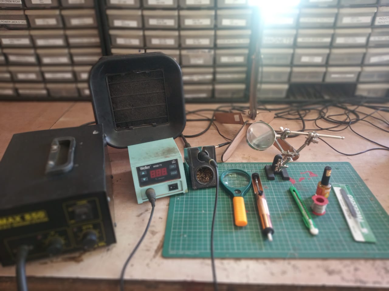
Soldering Corner:
Our soldering corners is comprmise set of Hot air gun,Soldering iron,tweezer,flux,solder Lead,magnify glass etc.


Componant List
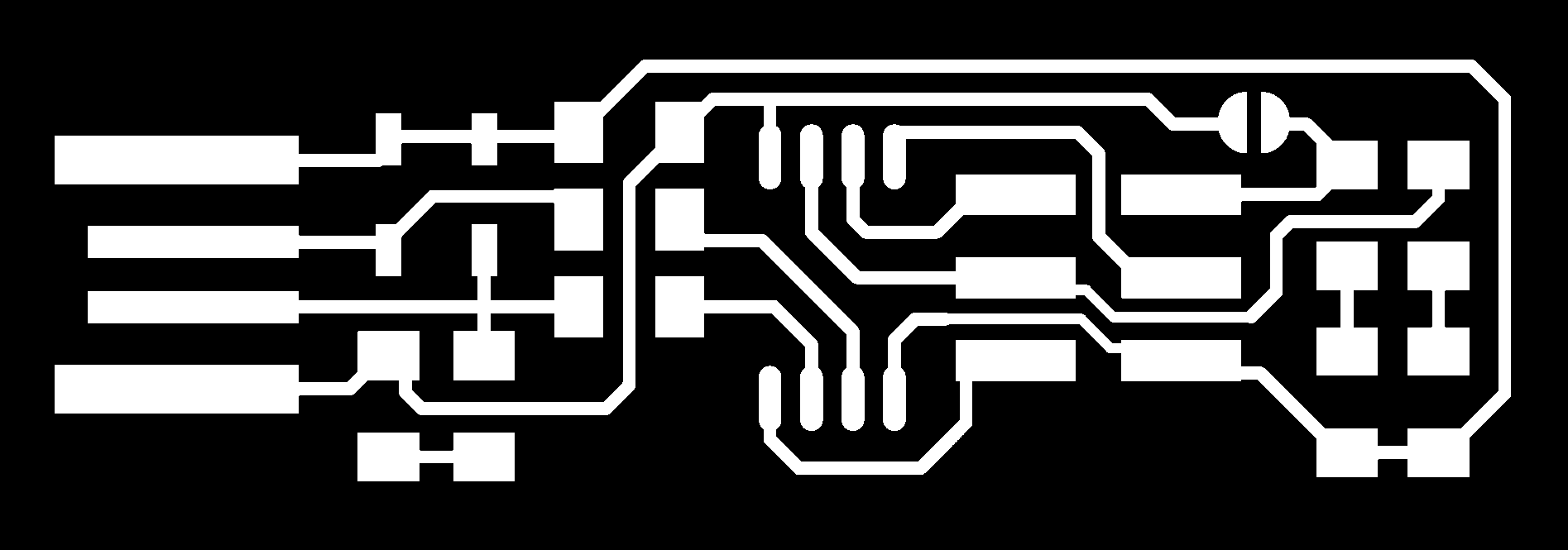
To mount the componants in correct orientation i referd brian documents where i got the circuits design both in schematic and PCB design as well.Using this design i can stuff my componats in correct place with porper polarity.
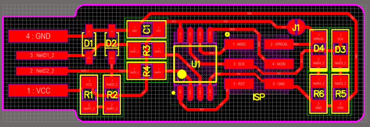
Brian Board
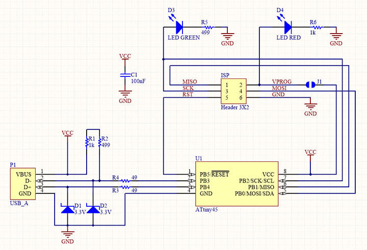
Brian Schematic
Soldering & stuffing
Before i start stuffing the componants on PCB first i put flux all over the track.As Neil mentioned to placed the componats inside out so first i choose ATtiny45 IC to fix on PCB folowed by 2 by 3 header.After that i placed resistors ,capacitors and diodes on PCB board.
I did one mistake here everyone should take care of it that is to choose proper value of componants i fix wrong diode that i got to know when i start to program my board there was errror that improper selection of componants. So i need to desolder it using hot air gun placed proper value of diode.
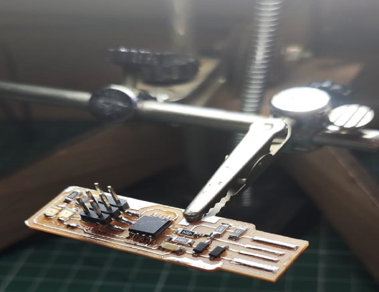
Finally i put extra solder on USB contacts make sure proper USB connection will estalblish. After doing all, i checked the LED whether it glow or not on multimeter . Hushhh all set!finally my FABISP PCB get ready to program by USBasp programmer.
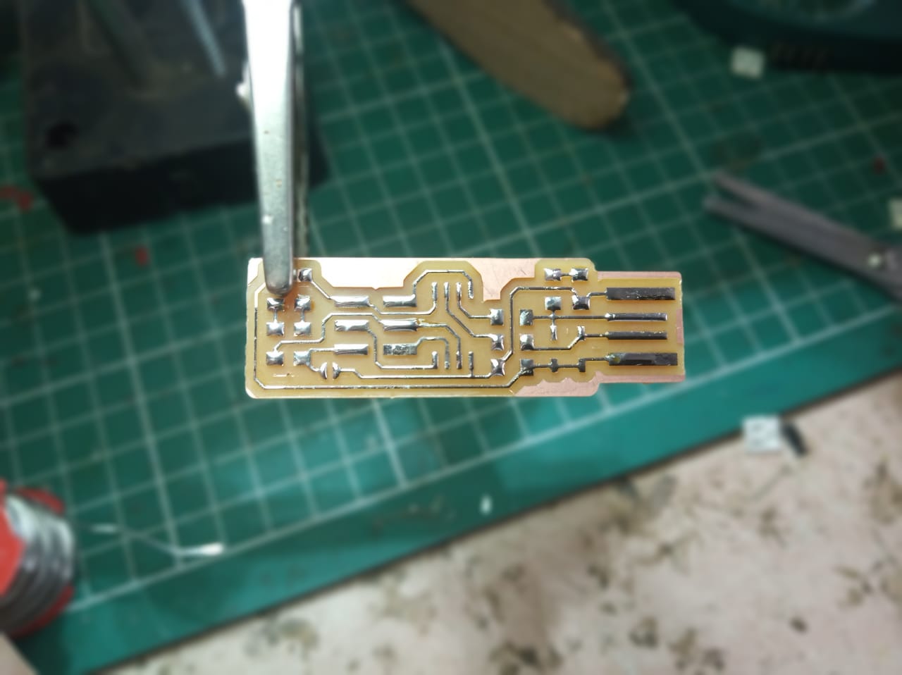
Soldered traces
Hero Shot
.
Step 4.Build Programmer
First i brought USBasp which is ready made programmer which i need to program my FABISP programmer.The USBASP is a serial programmer having Serial Peripheral Interface for programming .The programmer consists of 10 pin standard serial connector for connecting to the target board for programming.So i interfaced it with my FABISP board. Download driver for USBASP. Remember when you interface perticular pin to peripheral check the connection before going yo used it otherwise which may dammage your board.
Inteface USBasp with FABISP
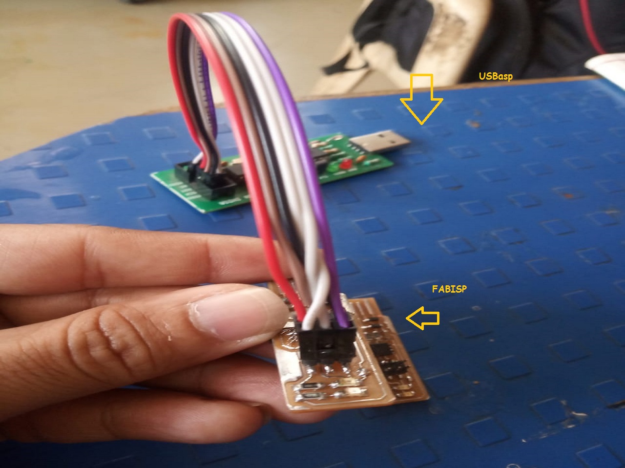
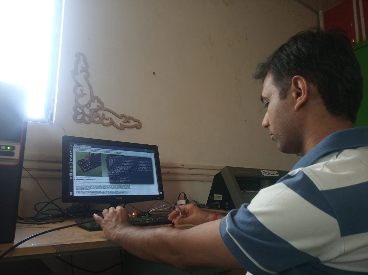
After proper interfaced i took USB extension cable to reduce the risk of damage to your built-in USB ports.Then i discuss with Lab instructor whether to go with LINUX or windows OS . So I choose Linux one and accordingly i begin my software installation process which i mentioned below.
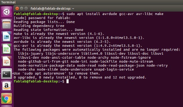
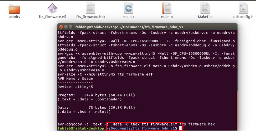
The reson to run make command is that our ATtiny45 understand the HEX file so to convert main.c file into main.hex file we used make command.
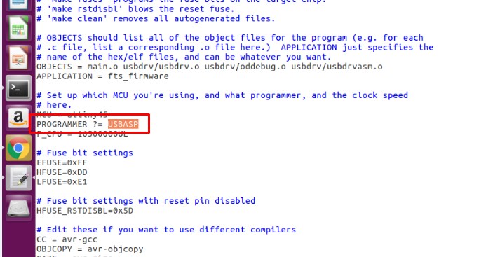
First i need tp program my ISP to behave as a programmer for that i need programmer to program my board.So update the makefile and put the name(usbasp) of USB programmer.
When we run this command we actually erase the our FABISP and then program the FABISP.This program will stored in flash memory ofit
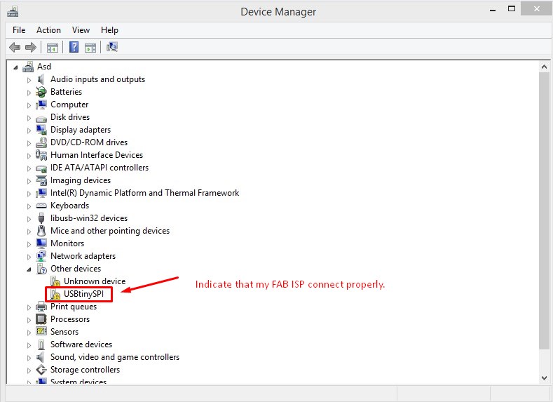
After running the above command i checked the my FABISP whether it acts as USB device or not.For that i removed my FABISP from programmer and then plug in to the USBport.Its works!properly.Also i used type command lsusb.Also i checked onto windows as well.
Below video shows the used of my FAB ISP to programmed the boards.Click here to see detailed information given in electronic design week assignments
.