7. Electronics design
Objectives
- Download and learn a PCB Design software
- group assignment : use the test equipment in your lab to observe the operation of a microcontroller circuit board
- individual assignment: redraw an echo hello world,
- Add (at least) a button and LED (with current-limiting resistor)
- check the design rules, make it, and test it
- And simulate its operation
PCB Design Softwares
- Altium
- KiCAD is an open sourse Electronic Designing Software
- Cadence
- Eagle from Autodesk. I chose to use this as I already have an auntodesk account for Fusion 360.
Eagle Software
EAGLE (Easily Applicable Graphical Layout Editor) is a flexible and expandable EDA schematic capture, PCB layout, autorouter and CAM program from Autodesk. EAGLE is popular among hobbyists because of its freeware license and rich availability of component libraries on the web. I have started this week by downloading Eagle software from this link. I logged in with my autodesk account as the files will be saved in cloud and can be accessed from other machines as well. As I do not have any experience with PCB design softwares, I pretty much followed what my instructor Yadu Sharon suggested. Yadu briefed us on how to install libraries, add parts, connect wires and edit schematic layout in Eagle and asked us to tryout any simple design before going into this week’s assignment. Here are the steps I followed to design my circuit .
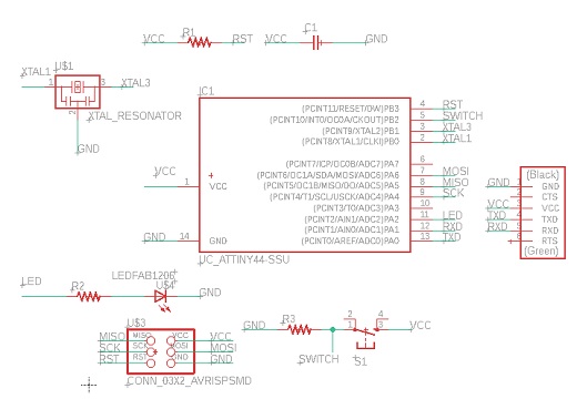
Components in the circuit
First i drew the basic Echo-board and next i additinaly added an LED and Push Button, on the PCB
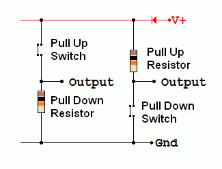
Pull-up resistors
Pull-up resistors are not a special kind of resistors;
They are fixed-value resistors which are used to ensure that a wire is pulled to a high logical level in the absence of an input signal.
They are connected between the voltage supply (usually +5V) and the appropriate pin, which results in defining the input or output voltage when there is no driving signal.
Pull up resistors pull up a pin to a HIGH state.
Pull-down resistors
Pull-down resistors also work like pull-up resistors, except that they pull the pin to a logical low value.
They are connected between ground and the appropriate pin on a device.
Pull down resistors pull down a pin to a LOW state.
Resistor Value
The appropriate value for the pull-up resistor is limited by two factors. The first factor is power dissipation. If the resistance value is too low, a high current will flow through the pull-up resistor, heating the device and using up an unnecessary amount of power when the switch is closed. This condition is called a strong pull-up and is avoided when low power consumption is a requirement. The second factor is the pin voltage when the switch is open. If the pull-up resistance value is too high, combined with a large leakage current of the input pin, the input voltage can become insufficient when the switch is open. This condition is called having a weak pull-up. The actual value of the pull-up’s resistance depends on the impedance of the input pin, which is closely related to the pin’s leakage current. However the resistance value for Attiny 44 is specified in its data sheet as 10KOhm to 20kOhm, We have opted 10kohm resistor for the pull-up.
Button part
In the button Section i added a Pull-down resistor, without the pull-down resistor we can’t get the actual value of the button.
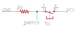
In my schematic R3 is the one pulled-down to ground.
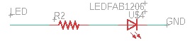
LED Part
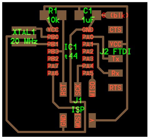
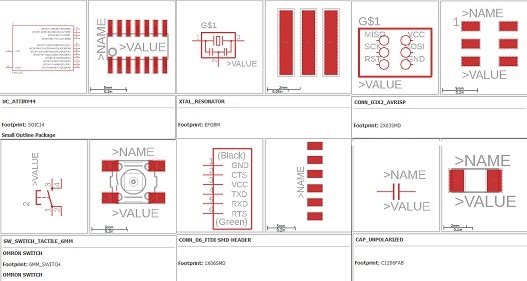
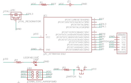
- ATtiny44 x 1 - This is a programmable microcontroller chip that controls all the parts on the board and is programmed from the computer. Let us say this is the brain of our Board.
- XTAL 20HZ x 1 - This Resonance crystal acts as an external clock for the circuit. It needs the input traces to be connected to two pins on the board and the ground trace to the GND circuit.
- Resistor 10K x 2
- Resistor 99ohm x 1
- Capacitor 10uf x 1 - this is a device used to store electric charge, consisting of one or more pairs of conductors separated by an insulator. This will help filter devices to remove voltage or signal spikes in our circuit.
- Push button x 1
- ISP header x 1 - the 2x3 pin header that connects the FabISP to our newly created chip(ISP - In System Programmer, I have alreay made a FabISP (In System Programmer) board, as part of completing an earlier week’s assignment)
- FTDI header x1 -the 1x6 pin header that connects to the special FTDI USB cable (FTDI is Future Technology Devices International - The company that makes a special usb cable - and drivers that let us write to the 6 pin output like a standard serial port.)This will connect the circuit to the computer to both read the program and power the board. It’s VCC and GND pins need to be connected to the respective VCC and GND circuits on the board, and it’s Tx and Rx pins connect to the two free pins on the microcontroller.
Designing Schematic Diagram
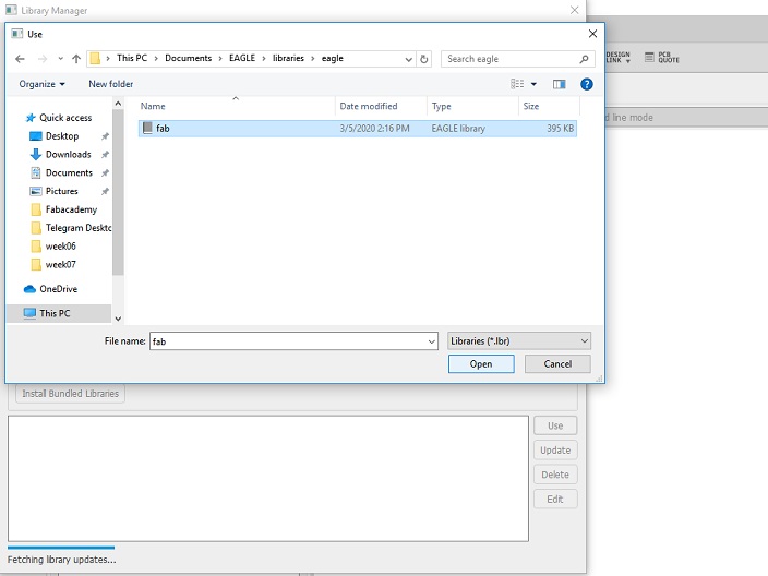
Step 1: I have installed the fab library from this [link](https://gitlab.fabcloud.org/pub/libraries/electronics).
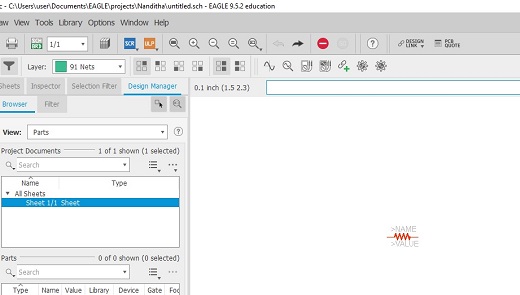
Step 2: - In Eagle, I have created a new project, by clicking File => New => Project and named it Nanditha then created a new schematic by clicking File => New => Schematic
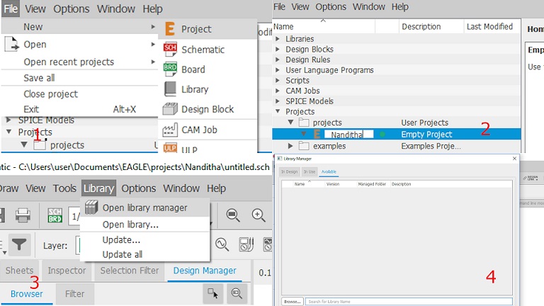
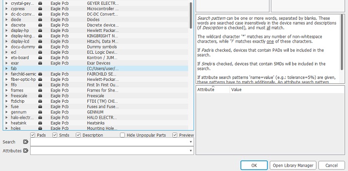
Step 3: go to Library > open library manager > In use > Browse > choose the library(give the path to fab.lbr) > open. The library then will be added and installed in the software.
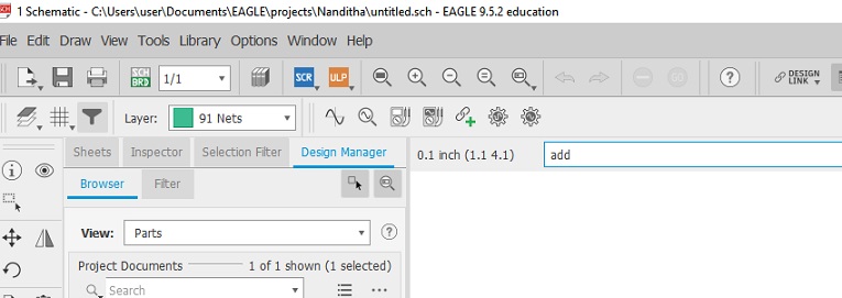
Step 4: In the command line (just below the menus at the top), type add
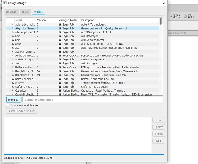
Step 5:The add window will pop up a long list and all libraries that are in EAGLE’s search path will be shown.
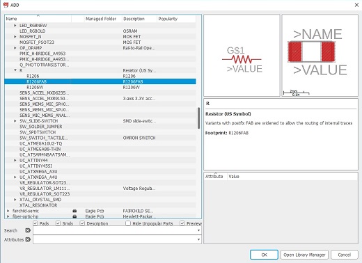
Step 6: Left click to place the component in the schematic.
Place this part in the center of your schematic. Press escape to return to the add menu, and then escape to exit the ‘add’ tool.
Step 7:Similarly add all other components.
Once all components are added the screen looks like this.
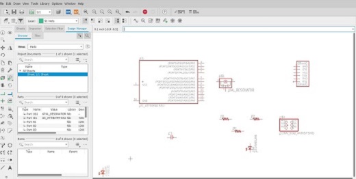
Step 8:The component can be moved, rotated and mirrored by clicking on the following icons from the tool bar,  then click on the component itself.
Step 9: There are 2 connection methods:
1. Drawing directly - For this, use the wire tool to connect all the components together - where there are overlapping AND connecting wires, be sure to add a connector point so that the schematic knows the wires are connected
2. Using Labels - Use the wire tool to draw a short wire and name it.
to connect all the components together - where there are overlapping AND connecting wires, be sure to add a connector point so that the schematic knows the wires are connected
2. Using Labels - Use the wire tool to draw a short wire and name it.
I used the second method of Labels. Reason is that it is more cleaner and won’t make much mistakes.
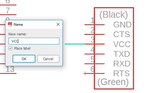
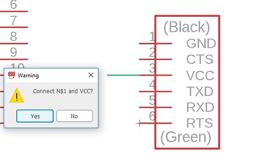
Step 10: Name the pins by typing name in the command line. Change the name to the desired(here VCC) in the popup.
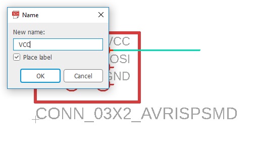
Step 11:Adding parts such as GND and VCC to pins which are connected to VCC or GND can help connect all the parts which need to be connected to either the VCC or GND circuits without having to have lots of wires crossed over
Step 12: Once all pins are connected, my final Schematic diagram looked like this.
Check for errors using ERC button  in the tool bar.
The output of my ERC check:
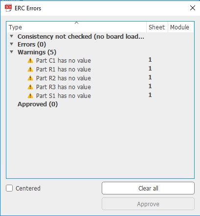
These errors can be ignored as I would be giving values to those components later.
Things to be careful while Creating Schematic Diagram
- The names of the components are very similar and can get changed very easily, So one has to be extremely careful while picking the components.
- Make sure that all connections are made/ labels given
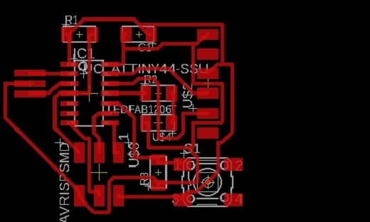
Designing PCB
The PCB components and connection is automatically generated from the schematic.
Step 1: From the file menu take Switch to Board option  and press it.
A board window will open up. If the schematics file is already not saved, it has to be saved at this point.
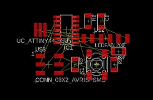
The board will show all the components with traces. The components I added will be jumbled up in a corner with yellow unrouted traces(airwires) attached. I can’t find the screenshot for this step.
Set Design Rules
Step 2: Change the design rules by clicking on the Design Rules button under Edit Menu
Here are the changes I made in accordance with our lab equipments.
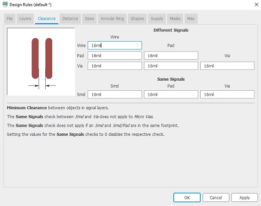
The bit we use here in Superfablab, Kochi for milling is 1/64 bit. So here the trace will come around 16 mil.
All clearance measurements have been changed from the default 6mil to 16 mil.
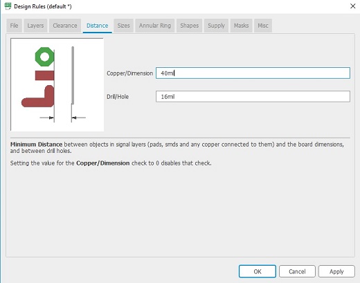
Hole Distance has been changed to 16 mil.
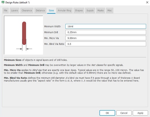
Minimum width of objects was changed to 16 mil.
Next we need to set the Size of the Copper Trace , in dafult 6mil, and we need to make it 16 mil.
Step 3:Start drag and drop the electronics components on the board to black area. Organize the layout of the components, rotate them and keep what is connected to each other next to each other to make the routing easier later on.
Once selected, right clicking will rotate the selected component.
Bring the components as close as possible to their connecting parts. By using the move tool, the components can also be moved in groups.
Step 4: Once components are more or less aligned and as close to their corresponding connections, the traces has to be made using the traces tool. Click on the centre of a component to start a trace, then right-click to change angles.
Routing
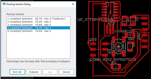
Step 5:I used Autoroute by pressing the tool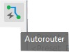 from the toolbox.
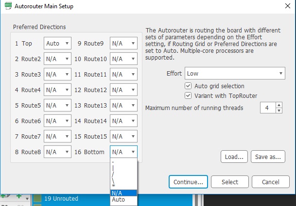
By default it comes with Bottom and Top layer , but here we are using One layer so used Top layer only.
Autoroute will suggest many routes, we can choose one that is suitable to us. When autoroute tried to optimise I only got 79.2% as the best optimisation.
Step 6:I gave “END JOB’ and removed all the routes by pressing “ripup;” on the command line. Then all the Yellow Lines were revealed like before.
Step 7: I started connecting each component manually using Route airwire tool. Once I was satisfied with the connections I gave, I tried to optimise it again. This time I got 85% as the best route.
Step 8: I went back to schematic and changed some pins.
Changes I made: SWITCH was connected to PB2 of microcontroller initially, I changed it to PA3. Just like in the first time, all changes are reflected on the board diagram.
I tried to optimise it again but I only got 95.8% as the best route. Just one line was not getting connected.
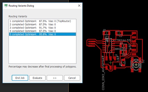
So I used Ripup tool and removed the lines near it and gave the connections manually.
When I optimised after this, I got three 100% routes.
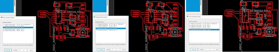
I chose the route based on the space it utilizes. Then I rearraged a bit to make the board look better.
Exporting a board design
Settings should be Monochrome and 1000 DPI - this will export an image with white traces.
The colour mode was set to greyscale Image ==> mode ==> greyscale
Step 9: In the menu, I took View and used the layersettings tool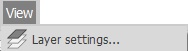 and made the top layer visible and hid all other layers.
Next I hid all the traces, pad names, via lengths etc. For this I took the Window from the menu and pressed 
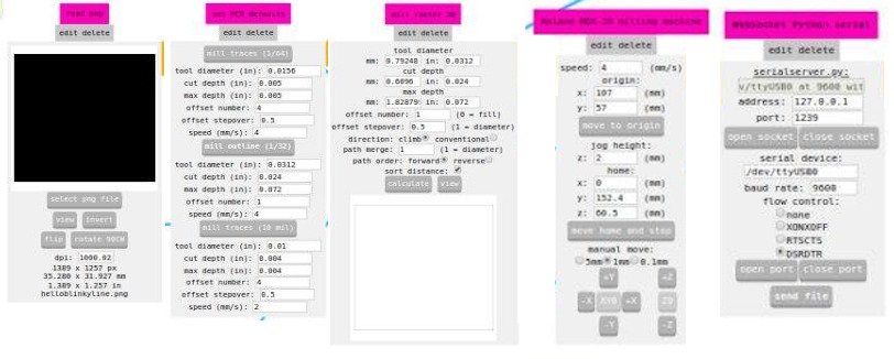
I exported the mill trace and cut trace in .png format using File ==> Export in the menu.
Things to be careful while Creating Board Diagram
- The crystal Xtal has to be very near to the microcontroller
- The ISP header 2x3 header pins need to be in the correct position as in the original diagram
- The FTDI header should be on one side
- The Resistor for the switch should be placed very near to it
- The resistor for the LED should be placed very near to it
Mistakes I made while Routing
- I didn’t set the design rules at the beginning
- If I had tried to do the manual routing at first I could have avoided a lot of trials.
- Learning routing requires patience and has a large leearning curve. But once I got the hang of it, it turned out to be fun.
Editing Board Files / Creating Traces and Mill-out Files.
I opened the .png file I exported from Eagle in GIMP
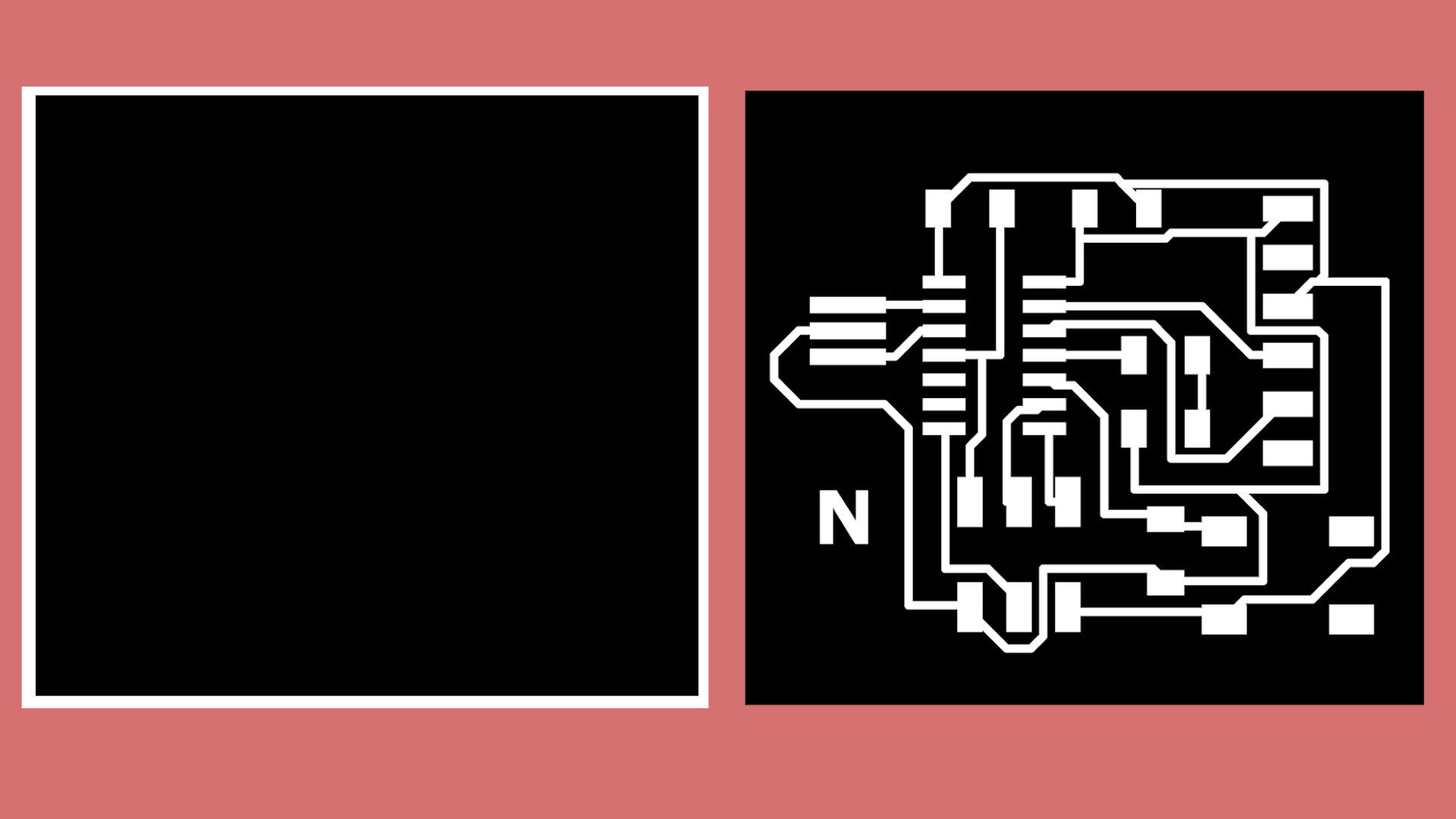
I added the letter N to one side of the board using Text Tool. I gave Sans-serif as font in Bold and size as 150 px and changed the text colour to white
Group Both these layers by pressing New Layer Group under Layer
Now drag and place both the Text N layer and the board layer under this group inside the Layers window
Select the area and press Ctrl+c and Ctrl+z
Now a new layer will be formed, delete the layer group.
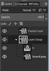
Give a White Background layer—
Select the necessary area using Rectangle tool(The area should be a little bigger than the trace to include the border as well)
Now Crop to Selection under Image in the Menu
Press Border under Select, A new window called “Border Selection” will pop up.
I gave the border size as 0.5 mm and style as smooth
Take the Bucket fill tool from the Toolbox and select the foreground colour as Black—
Now fill the colour by pressing the bucket tool in the selected border area on the background layer.
Hide the background layer and export the .png file helloblinky
Then hide the Trace Layer and export the .png file helloblinkycut
 —This is the changed documentation after Mr.Puneeth Raj pointed out a mistake that all of us at Superfablab, Kochi is practicing. For details check under the section Mistakes that occured below.
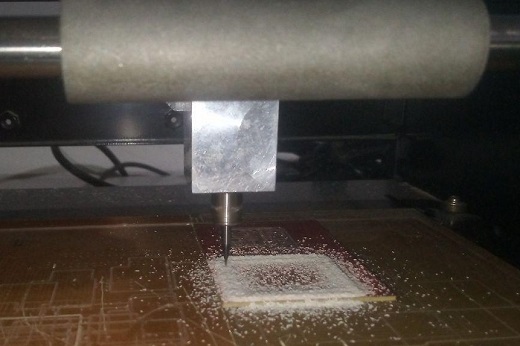
Milling
This method was exactly like how we did in PElectronics Production week.
I took Mods interface to connect with the Roland Modela MDX-20 to mill.
I chose 1/64 bit to trace on the board.
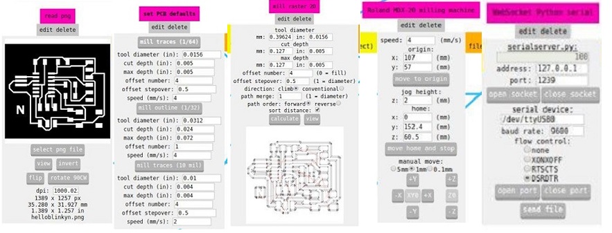 Cutting was done using 1/32 bit.
 Here is the milling happening.
Things to Remember
- The Mods cuts out the Dark portions and leaves White portions.
Mistakes that occured
- I milled on the same PCB as Nibin Baiju, and when his outline was being cut, due to the error while giving origin, it accidentally started cutting one end of my trace. I could save my board without causing much damage.
- While I gave the border in GIMP I didnot add the kerf of the mill while adjusting the space between Trace space and Cut Space, Hence that spacing was too narrow and I had to give the trace line a bit of soldering to make sure it will work properly.
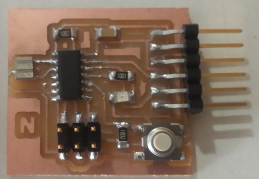
Soldering
While soldering I placed the ATtiny44 first. I soldered the left end then the diagonally opposite right end, followed by the opposite end on the left, and then the diagonally opposite right end and so on.
After that I placed a bit of soldering lead on all the pads at first, then started soldering each component in its place.
// The order of soldering I followed was
Track Test
Before programming the board, I checked that there were no shorts with the multimeter. The multi-meter will save a lot of time going crazy debugging if we are certain that our circuit is not working as it is supposed to.
Multimeter Fluke101
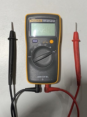
The multimeter we use in our lab is Fluke 101.
To restart the multimeter, turn the rotary switch back to the OFF position and then to a necessary position.
Checking for continuity
Turn the dial to resistance (Ω) mode, Push the YELLOW button once to activate the continuity mode.
With the test probes separated, the multimeter’s display will show OL.
Connect the test leads across the component being tested. It is best to connect the VCC connections and ground connections first, and then the connections to each pin on the micro-controller.
The digital multimeter beeps if a complete path (continuity) is detected. If the circuit is open (the switch is in the OFF position), the Multimeter will not beep.
Connecting Hello Blinky to the ISP programmer
Now connect the ISP programmer that we made earlier, to the other USB port. Use the ribbon cable to connect the FabISP and the Hello Blinky board using the two six-pin headers soldered on each.
Then I took the Control Terminal of the Laptop and inserted the code
avrdude-c usbtiny -p t44
And the result is this:
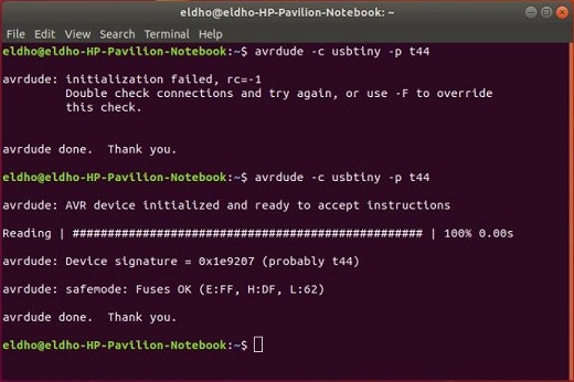
Mistake made while connecting the Hello Blinky Board.
Initially I made the mistake of not connecting together the Ground pins of both FAB ISP and Hello Blinky. Hence the initialization failed. When I gave the connections correctly, the device initialised.
Programming Hello Blinky
I programmed my Hello Blinky Board using Arduino Software. Here is the output:
What made me Proud
Although it took me a while to learn the routing, I was able to do manual routing. I was very patient with the soldering and got it done correctly. I was really happy when my instructor Jogin Francis commented that it looks nice. The N that I added to one side also made it look cute and I was happy with my design choice. I also realised that I started enjoying GIMP and now finds different ways to reach the same goal
Fabkittens
We found these two crying and really malnourished inside a box filled with equipments inside our Superfablab. I started taking care of them today, 11th March.