5. Electronics production
This week we started the electronics side of the course with PCB fabrication.
Objectives
This week we have to do a group assignment to characterize the design rules for our PCB production process: document feeds, speeds, plunge rate, depth of cut (traces and outline) and tooling and document our work.
As individual assignment I have to make an in-circuit programmer by milling and stuffing the PCB, test it, then optionally try other PCB fabrication process.
Group Assignment
Find it here
Individual Assignment
For individual assignment I have to learn the details of the milling machine in our lab to mill a programmer.
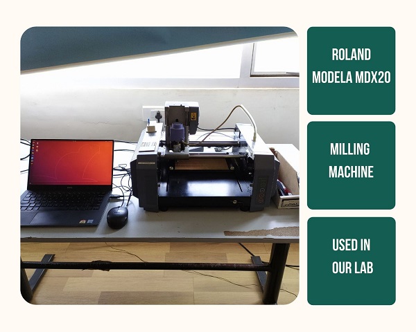
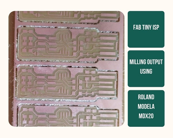
Roland Modela MDX-20 - Machine used in our lab for PCB Milling
PCB Materials used in our lab
FR 1 - Phenolic Cotton Paper (FR means Flame Resistant)
It is a hard, flat material that consists of a thin layer of copper glued over a paper with non-conductive phenolic resin . The thickness of the FR1, Phenolic cotton laminated sheet, in our lab is 1.8mm and it is brown in colour.
FR 4 - is a glass fiber epoxy laminate - Used for chemical etching. FR4 uses 8 layers of glass fiber material.
Parameters
- Cutting surface : The surface of the solid object to be cut
- Size : The size of the finished object
- Depth : The depth of cutting
- Material : The composition of the workpiece to be cut
- Cutting process : The stage of cutting
- Tool : The diameter of the cutting tool and the shape of the tool’s tip
Bits used for milling
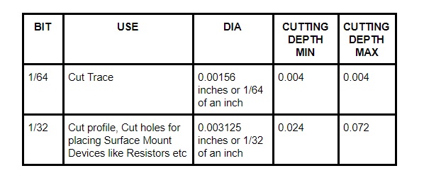
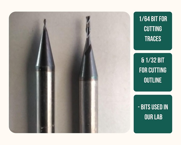
Along with the machine, we need to get the right tools for milling PCBs. The very critical part of these is the engraving bit, which creates the actual traces onto the PCB. The bits used for this purpose have to be sharp enough so that it can cut through the copper as opposed to tear it and yet it needs to be very fine and creates small footprints to mill the tiny traces. The bits used for cutting in our lab are made of carbide. Bits available in our lab are 1/8, 1/32 and 1/64, but we did not use 1/8 bit.
Sacrificial layer
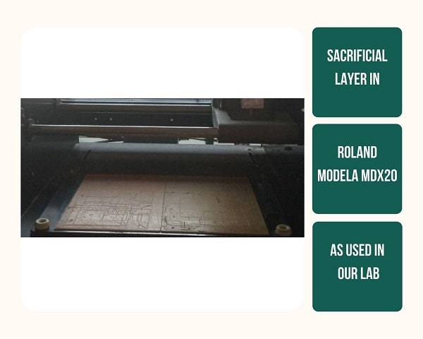
It is, as the name suggests, a layer that sacrifices itself for saving the base plate from any damage ie, in case something goes wrong and the milling goes further than expected and mills onto the lower layer. Although many sacrificial layer materials are available commercially, what we use in our lab as a sacrificial layer is a PCB kept in reverse because its thickness won’t damage the bits and is very cost effective as well. To make a PCB into a sacrificial layer a dual sided tape was applied onto its copper clad board and carefully pasted onto the base plate applying sufficient force ensuring it is on level. The sacrificial layer has to be the same or greater size of the workpiece that is to be milled. Random designs are first milled on to the sacrificial layer to ensure the level of the workpiece.
Control Switch Panel
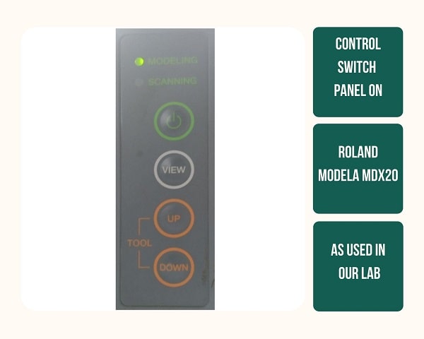
- Modelling Mode LED
- Scanning Mode LED
- Power ON/OFF, Standby Key
- View LED
- View Key To inspect board, the head moves away to the max of Y axis and the base plate moves towards the min of Y axis(front), so that object can be placed/ seen on the cutting surface
- Tool Up Key - Tool moves in the z axis towards max
- Tool Down Key- Tool moves in the z axis towards 0
The Machine Coordinate System
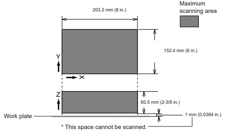
Here, the X, Y, and Z axes refer to the machine’s motions. When viewed from the front of the machine, the X axis runs from left to right, the Y axis runs from front to back, and the Z axis runs up and down, vertically perpendicular to the other two. In this machine the Bed is the Y axis, and the spindle movement shows the Z-axis.
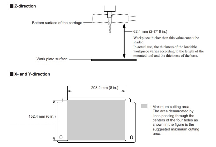
Maximum cutting area of the Machine
Coordinate Measuring Machine
Machine also acts as a coordinate Measuring Machine(CMM)
It works in much the same way as the finger of our hands when it traces map coordinates; its three axes form the machine’s coordinate system. Instead of a finger, it uses a probe to measure points on any object placed on it. Each point on the object is unique to the machine’s coordinate system.It then combines the measured points to form a feature that can now be related to all other features.
Alignment
The process of relating the two coordinate systems is called alignment.
Milling the Circuit
Required Items
- Milling Machine - Roland Modela MDX 20
- FR-1 PCB Board
- Computer to be connected to the machine to run the interface
- Bits - 1/64 and 1/32
- Allen Key
- Double Sided Tape - Netto
- Vacuum Cleaner
- Cloth Piece
- Cleaning Solution (If Required)
- Scissors
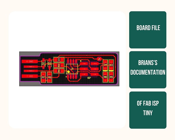
- Fab Tiny ISP design downloaded from Brian’s page Link to Brian’s Page
The mechanical setup
Step 1: Go to "view mode" by clicking on the view button on the Modela
Step 2: Clean the work surface thoroughly using the blower and surface cleaner.
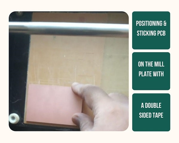
Step 3: Tape down copper board at o,o position ( 1 inch x 1 inch from bottom left corner) using the double sided tape. We used Netto Tape, which is rather thin yet strong.
Step 4 Loosen existing bit with the provided allen wrench.
Step 5 Put 1/64 inches bit in the modela, which is 0.0156" decimal. Set it up as high as possible in the machine. This part needs to be very carefully done as the bit might fall from our hands and get broken.
Step 6 As a precaution we placed it from bottom up, in a way so that it will only fall into our hands. Besides, we kept a towel underneath as a safety net.
Step 7: Clear out the memory of the Modela, by holding the both ""up" and "Down on the machine.
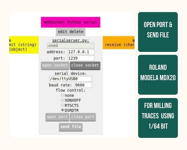
Now instructions to make a toolpath are given through the Mods interface.
Mods Interface
Just as in the case of Vinyl Cutter we used Mods Interface and not the software given by the manufacturer to interact with the machine. Mods interface is a set of software tools for personal fabrication which can be used with machines common to fab labs around the world. It is maintained by the Center for Bits and Atoms, MIT. Mods
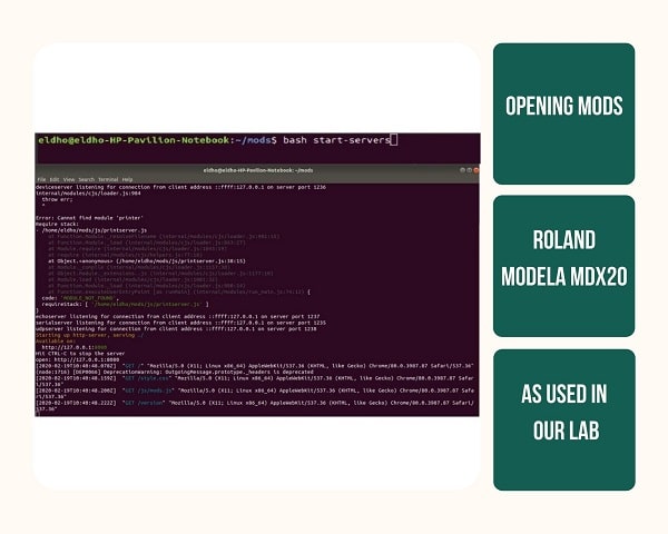
Step 8: The command bash start -servers is given on the command prompt, the mods page will open up in the browser. As I did not bring a laptop to the lab, I had to borrow from Eldho Kurian, my fellow fab academy student.
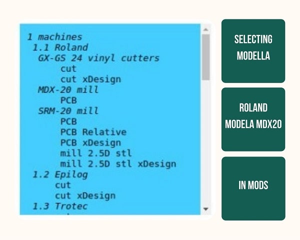
Step 9: In programs-1 Machines Roland Modela MDX-20
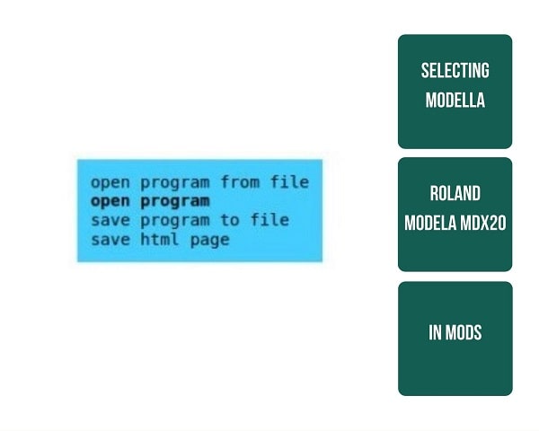
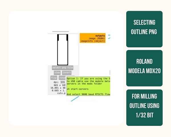
Step 10: Load the image as a png or svg file
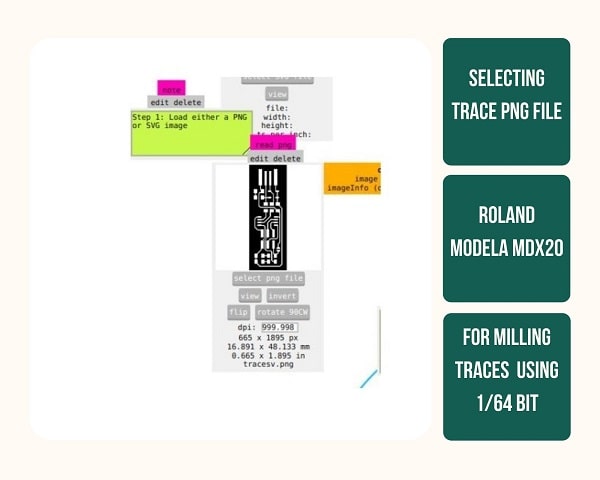
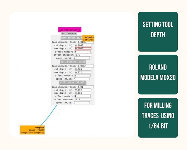
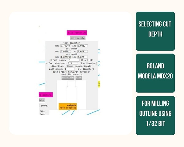
Step 11: Set PCB default settings if required, Select the bit, here 1/64 and adjust the depth.
mod7 PCB defaults
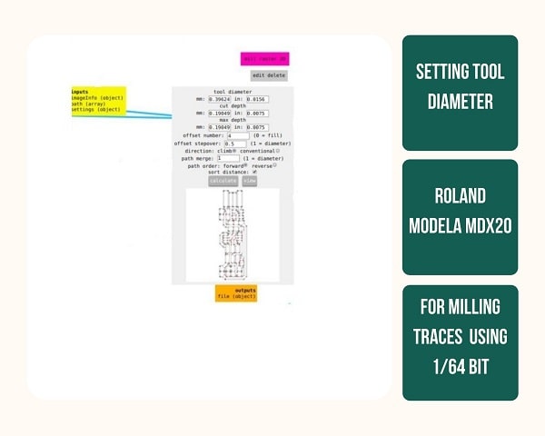
Step 12: The raster image is made and shown based on the inputs we have given already That output ia a vector file which can be viewed
mod10 nodes
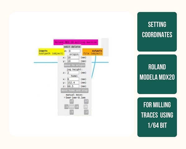
Step 13:Set origin by specifying the starting points where the workpiece is kept. Here x = 10, y = 10 and move the spindle to the origin
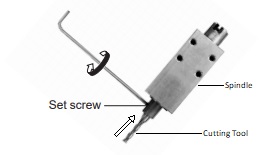
Lower bit close to the origin by pressing the “Down” button, and stop without letting the bit actually touch the surface.
Loosen the hex screw that holds the bit and lower it until it touches the top surface of the board.
Lower it slowly so the bit doesn’t fall into the board and break.
Now that the bit is at surface level, tighten screw. The bit has a tendency to move up while screwing, this may end up in partial or no milling.
So the bit has to held tightly in place while tightening the screw.
Step 14Open Mods again and then send file to machine.
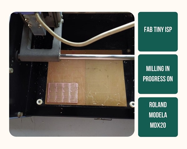
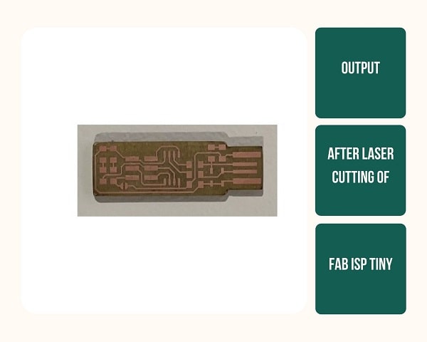
Output
Challenges
The most challenging part of this process is to get the correct cutting depth. The bits yield a wider cut the deeper you go, effectively robbing you of precious engraving resolution. If the right depth is not tuned in, some traces will come out too thin and frail.
I had to try out a few cutting depths and had to readjust the height of the bit to the correct position, ie. the tip just touching the plate.
Here is the list of various cutting depths I tried out.
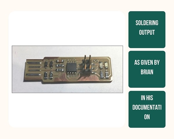
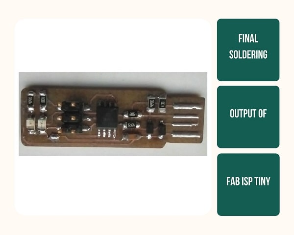
Soldering the Circuit
Objective:
- To solder all the components on to the Milled PCB and create a Fab ISP programmer ready to be programmed as given by Brian
- Track Test it and ensure it is working.
- Connect it to the USB port of a computer and ensure the Power LED switches ON
Soldering
Soldering is the process in which two or more metal items are joined together by melting a filler metal, with relatively low melting point, and then letting it flow into the joint and acts as a permanent glue. It is done to form a permanent connection between electronic components.
Only the solder melts and not the parts that are being soldered.
Materials used for soldering
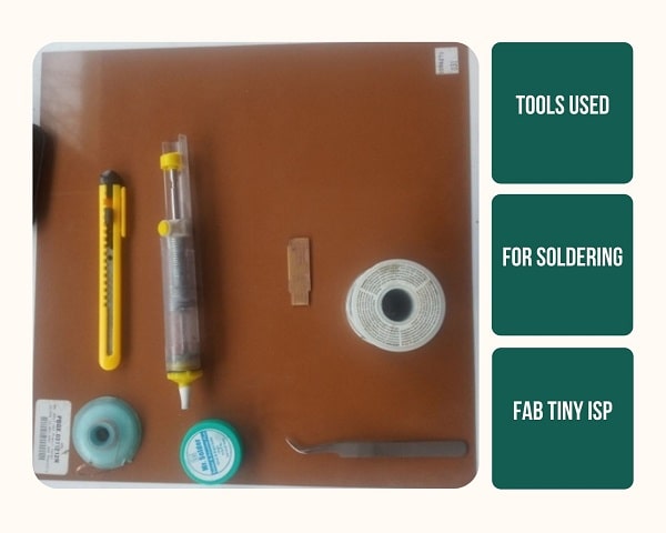
- Soldering Iron - very expensive iron, costs around Rs 15000/-
- Flex - to give viscosity for soldering and for surface cleaning
- Tweezers - To keep tiny components in place
- Soldering Lead - Solder is a fusible metal alloy used to create a permanent bond between metal workpieces, an oxymoron here because it is lead free solderThe melting temperature of the lead-free soldering lead used in our lab is about 217°C.
- Desoldering Pump - for removing through-hole components
- Soldering wick- Braided copper wire used for drag soldering (IC Soldering) and desoldering.
- Pen knife - To isolate and clear trace after soldering
- Fume Extractor
- Magnifying glass
- Lamp
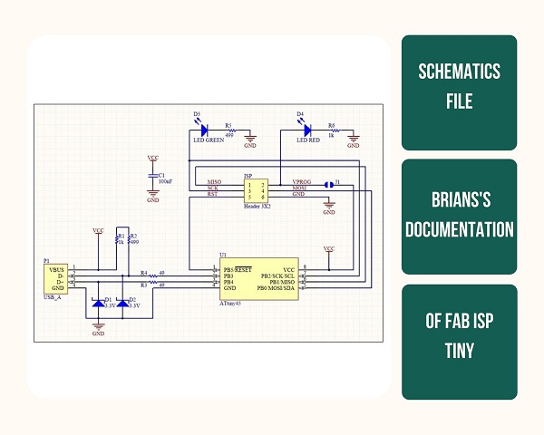
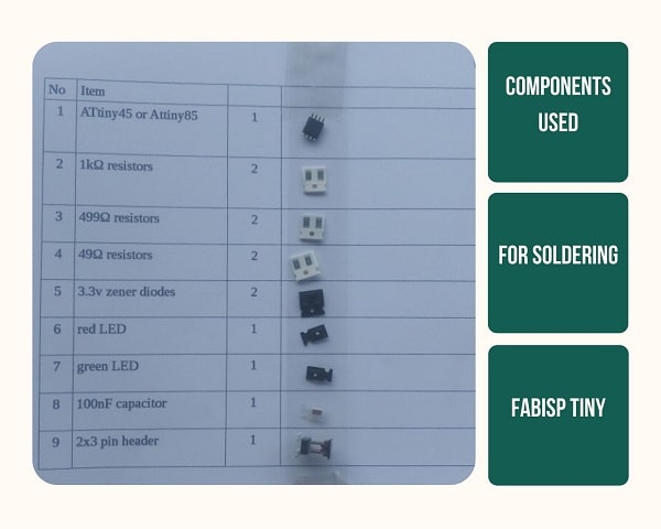
Components used for soldering FAB ISP
Board file shows where each component is placed. It is made from the schematics file.
How to identify Positive and Negative Sides of components
1. Attiny45 microcontroller chip - The dot on the chip should be at the same side and direction as the dot in the Board File
2. Zener Diodes - The silver colour line on the diode should be at the same side in the Board File. This is the cathode.

By connecting Cathode to positive and Anode to Negative, here we are reverse Biasing the zener diode. Ie, this diode with a Reverse Biased voltage of 3.3v will act as a voltage regulator. If we input 2v, the output will be 2v, if we input 3v the output will be 3v. But if we input anything beyond 3.3v, it will still be 3.3v. When connected to the USB port of the computer, iIt takes the input 5v and gives an output of 3.3v 3. LED - The Cathode, negative side has a thin green line. So the thin green line should come in the area where the Board File has a thicker line.

Clamps
The soldering workpiece can be held using three methods in our lab.
- Clamp PCB with tightening screw
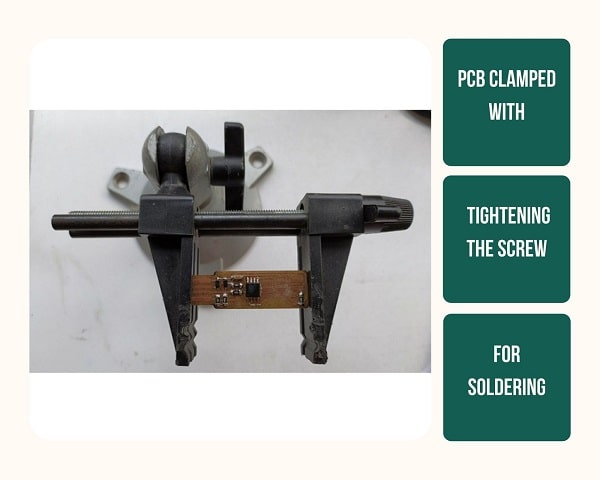
PCB Clamped with tightening screw
- Clamp PCB with crocodile clip
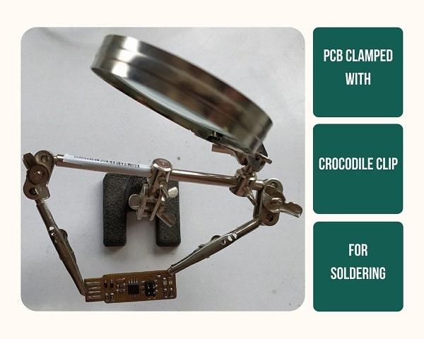
PCB Clamped with clip
- Fix PCB on a table using double sided tape; we used Netto tape.
Soldering Process
Step1 - Solder needs a clean surface on which to stick. So clean all the surfaces.
Step2 - To solder, heat the end that needs to be connected with the tip of the soldering iron(by holding soldering iron like a pen on the handle) for a few seconds, then press the tip of the solder(Atiny dip of flex on the tip is good).
Step 3- Important - Apply heat on the connection, not the solder.
Step 4 - Ensure that a good connection is created
Step 5- Let the solder melt and create the joint, but don’t let excess solder. It just needs enough to make a connection.
Step 6- Remove the solder tip and the iron.
Step 7- Let it cool for a few seconds.
Step 8- Make sure that the connection is not overheated, as it might damage the component that is being soldered.
Step 9- If the connection has excess solder then reheat and use the copper wire to remove it.
Step 10 - Wipe the tip of the iron on a damp sponge to clean it. The tip should now be shiny.
Step 11 - Unplug the soldering iron when it is not in use.
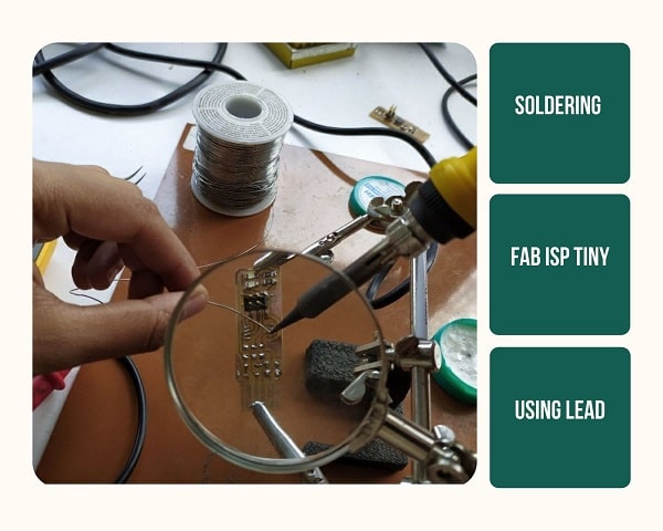
Soldering Using Lead
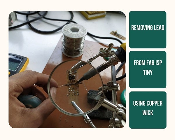
Removing Using Copper Wick
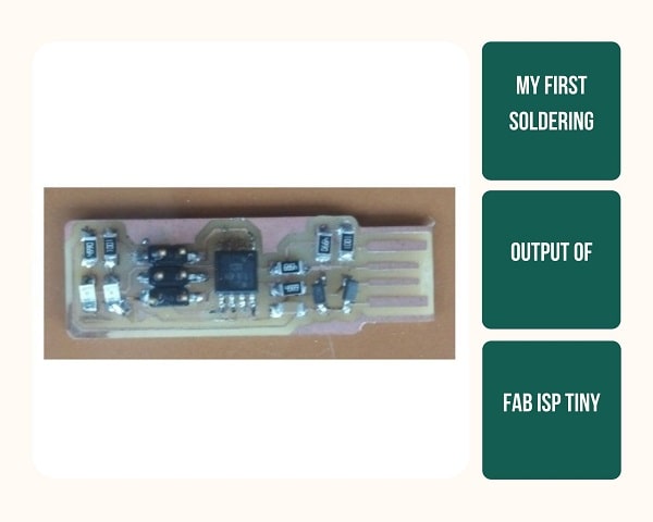
My first Soldering attempt, looked very bad, So I remilled and re soldered it.
Things to be careful while soldering
- Keep the temperature at about 320-350 degree Celsius
- Clean the tip always
- Use ample flex material
- Be careful about positives and negatives
- Keep only 1 component outside at a time
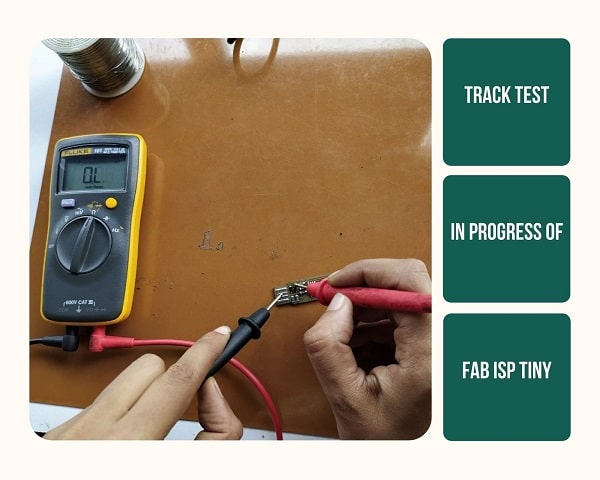
Track Test
Whether unwanted joints occurred or any needed were removed. If any joints are removed, do patchwork using soldering and create continuity I tested it with multimeter.
Software Installation
Once I finished the track test, it was time to program the board with the correct firmware.
Detailed debugging steps are provided in the Fab Tiny ISP documentation page.
For Ubuntu and other Debian-based distributions, enter the following command, followed by your password when prompted:
I downloaded the firmware source code firmware source code and extract the zip file (on Linux, unzip fts_firmware_bdm_v1.zip). Open the terminal and go to the directory by using the ‘cd’ command. Once in the directory type ‘make’and click enter. This will build the .hex file that will get programmed onto the ATtiny45. When the command completes, you should now have a file called fts_firmware.hex.
The make file of the firmware assumes that you are going to use a programmer in the usbtiny category (another fab ISP). If you’re using a different programmer, first figure out what avrdude (the programming software) calls it.
Edit the file called Makefile. It is important to use a text editor intended for programmers. Near the top of the file, find the line that says:
PROGRAMMER ?= usbtiny
change usbtiny to whatever programmer you’re using.
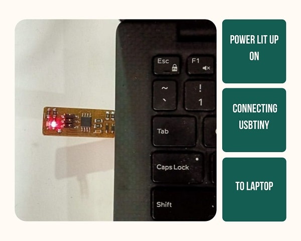
Plug the board into a USB port. USB2.0 is preferred over 3.0 if you have one, and use an extension cable so that you do not put strain on your board especially if your port is upside down. If you installed the red LED, it should be lit up now. If not, check the solder jumper and make sure that it is bridged. If your computer complains about a USB device drawing too much power, unplug the board and check for shorts.
Connect the programmer to the ISP header on your board. Note that there are two different orientations in which you can connect the cable; it is imporatant that you get pin 1 in the right place. Pin 1 is the MISO pin and it should be connected to the MISO pin of the board you are programming.
Type
In terminal and ensure the device is identified
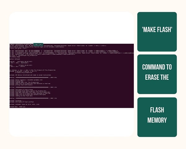
After in the terminal run the command ‘make flash’. This will erase the target chip and program its flash memory with the contents of the .hex file you built before. You should see several progress bars while avrdude erases, programs, and verifies the chip.
If something went wrong, check:
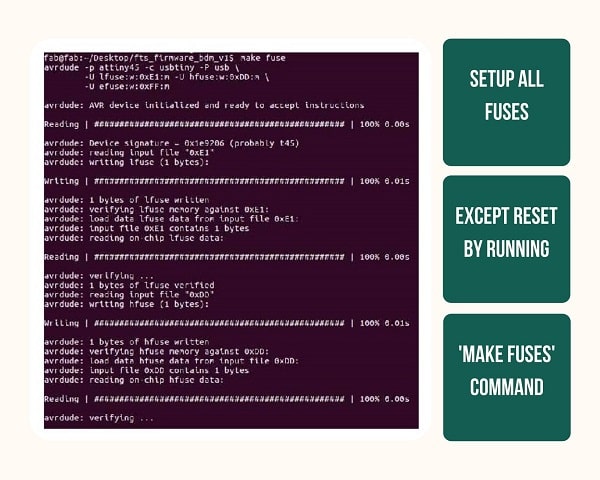
Once you’ve successfully programmed the flash memory, it’s time to set the configuration fuses:
First, we’ll set the fuses that control where the microcontroller gets its clock source from. This will allow us to check that the board works as a USB device, but it won’t yet be able to program other boards.
Only after confirming that USB works, we’ll set the fuse that disables the reset pin and turns it into a regular GPIO pin. This will let the chip use the reset pin to program other boards, but will disable the ability for this chip to be programmed again.
Go to the terminal and run the make fuses command. This will set up all of the fuses except the one that disables the reset pin.
type
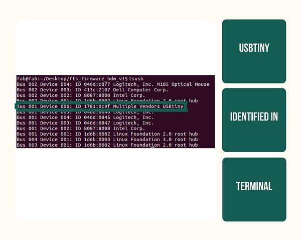
check wether the programmer is detected. If you see a “Multiple Vendors USBtiny” device, then the programming has worked. If it didn’t, the dmesg command might provide more info on what went wrong.
We need to change the bit that will turn the ATtiny45’s reset pin into a GPIO pin.This will disable our ability to reprogram this ATtiny45 in the future, hence make sure everything is working before doing this. Connect your ISP programmer to your board one more time, and in the Terminal run
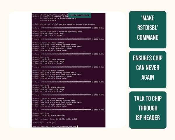
This does the same thing as the make fuses command.with that, avrdude will never be able to talk to this chip again through the ISP header. Now our programmer is finished.
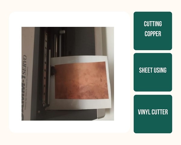
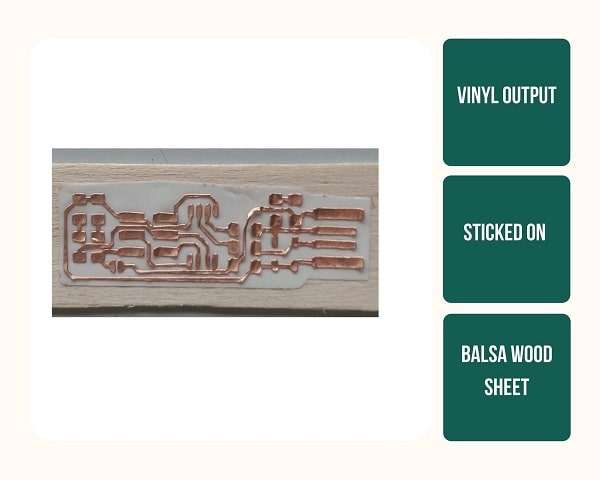
Vinyl Cutting of PCB
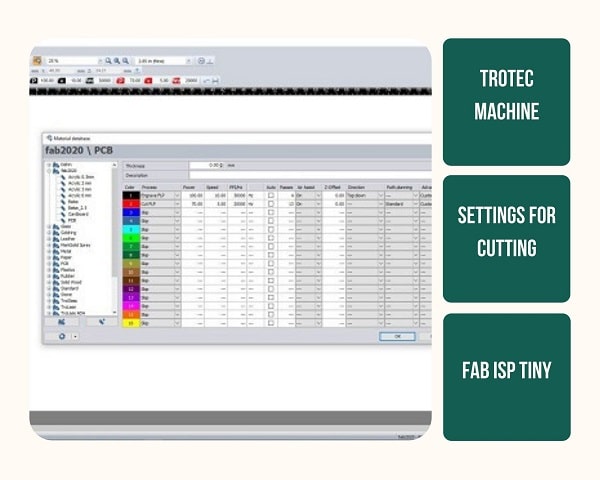
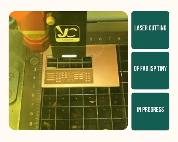
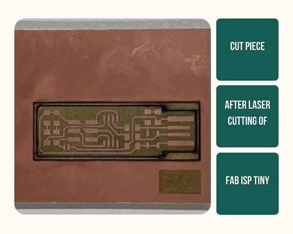
Laser Cutting of PCB
We were able to do laser cutting PCB as well because our lab has a Trotec speedy 400 Flexx CO2, Fiber Laser with Power 60-250 Watts CO2 60-120 Watts Flexx and Laser Power Fiber is 20-50 watts
Mistakes made
While Milling
- The first time I did the milling, I started cutting without bringing the head down to the origin, so it started doing the cutting motion at a height. So I had to stop and start over.
- While starting over, even though I have recalculated and done all other steps, I had to close socket and open socket operations, or the machine will not read the new instructions but will continue the milling it was already doing.
-
Although I was careful about origin and how much the workpiece will extend in the x -axis from the origin I set, I did not care about the extent on y-axis from the origin. The cutting was done outside
Learnings -
Size of design should be lesser than the size of the design
- Check the orientation of the workpiece and the design
- Check the smoothness of the bed
- Placement should be parallel to axis
-
Setting up and Drill Time -The first boards that have been produced took approximately 45 minutes -1hour to route and Mill . Quicker times have been achieved later on. A lot of time was wasted because the sacrificial layer was not in place correctly. Once the routing was completed the milling time for 1/64 tracing took about 8 minutes and cutting using 1/32 took about 2 minutes.
While Soldering -
First time I used a lot of lead and ended up having devices which were sitting on top of a tiny mountain of lead. According to my instructor, I had a flying diode. I’m also certain I ended up destroying the 2x3 Header.
- The second time I soldered I was stingy with lead and ended up not having enough lead at some parts. So I had to resolder those parts to enable connection.
- The copper I used to remove the lead was not clean and ended up causing more lead on the board.