5. Electronics production
This week’s achievement was milling, soldering and programming an in-circuit programmer.
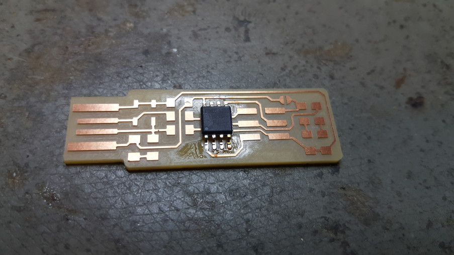
Milling
Preparing the data
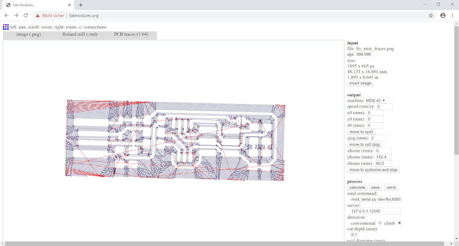
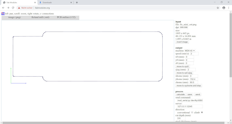
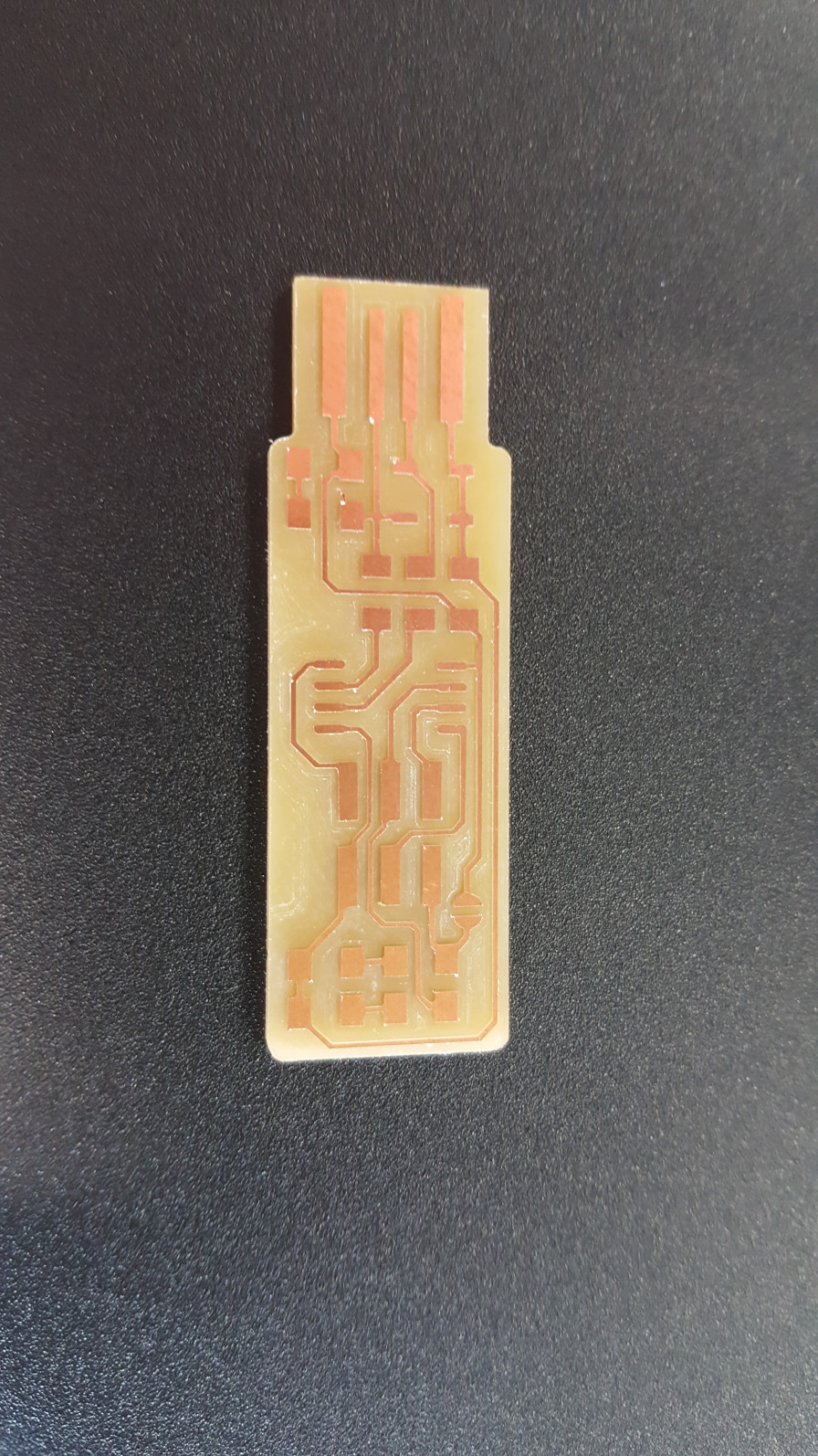
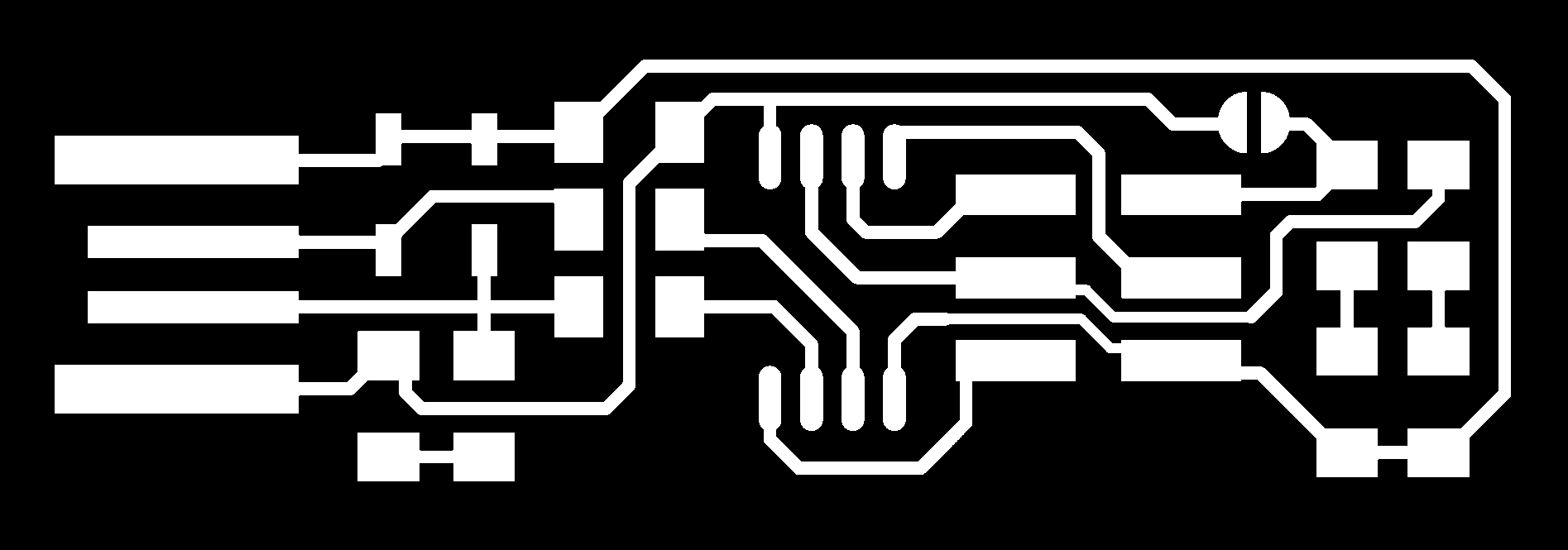
First step to mill a printed circuit board (PCB) was coming up with a virtual model of the traces and the shape of the PCB. Therefore, I downloaded the virtual traces and outline cutout shape of the PCB from the internet in form of .png images with a resolution of 1000 dpi:

I used fabmodules.org to upload the .png images successively and to generate the G-code for the CNC mill to mill the traces and to mill the outline shape ob the PCB.
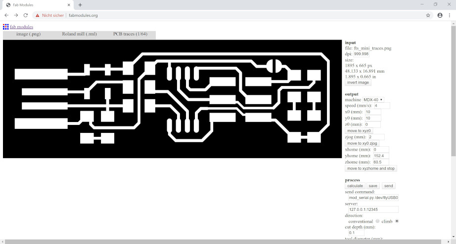
For the input file format I picked .png and chose the downloaded traces file. As an output format I picked “Roland mill (.rml) and as process “PCB traces (1/64)”. It means that the mill will cut the traces with an end mill with a diameter of 1/64” and the milling path is calculated accordingly.
Then the right milling machnine is chosen in the dropdown list. In my case it’s a Roland MDX-40. Speed was set to 2 mm/s and x0 and y0 to 10 mm. The number of offsets is set to -1 to remove all of the unnecessary copper material from the PCB. A mouseclick on the calculate button then lead to the milling path that has to be saved.
The same was done with the file for the outline of the PCB with the differenc that “PCB outline (1/32)” was picked as process.
Milling the board
The file then is opened in the software Roland VPanel for MDX-40. The rpm is set to 8500 rpm.
For milling the traces the 0.8 mm mill bit is mounted. Therefore, the mill head is positioned hogh above the mill bed. The used mill is a Roland MDX-40.
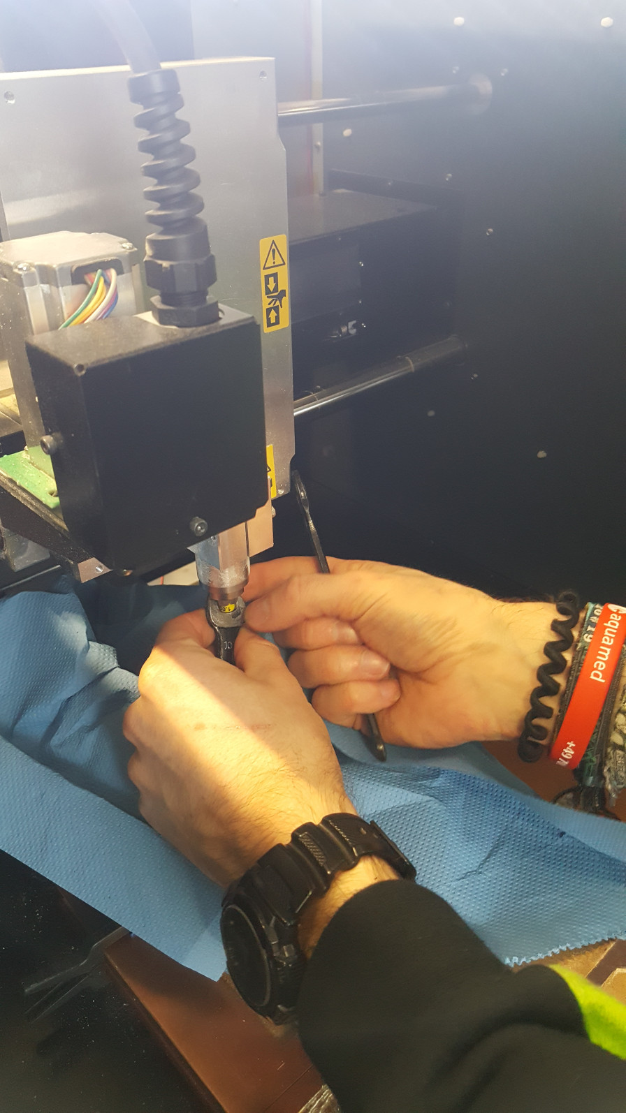
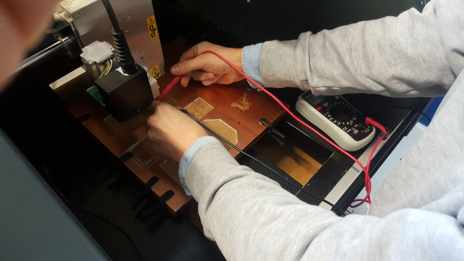
Then the x0,y0 and z0 are set. Therefore, the mill head is positioned above the PCB material where the bottom left corner of the workpiece should be. The tip of the end mill is then placed marginally above the surface of the workpiece. It is then succesively lowerd step until it barely touches the surface. That can be detected with a multimeter my measuring the resistance between the electrically conducting end mill and the electrically conducting surface.
The x, y and z origins are set to the current values. Then the milling can start.
After milling the traces of the PCB, the cutting of the outline can be done once the mill bit has ben changed to a 1.5 mm end mill and the z origin is set respectively.
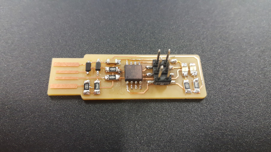
Soldering
After milling the board, stuffing the PCB can begin. Therefore, all the needed components were sticked to a labelled piece of paper with double-sided tape.
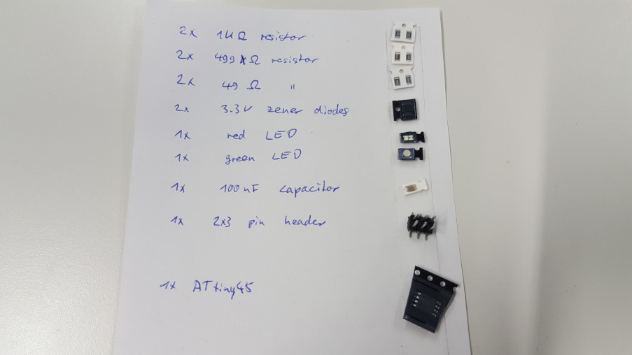
According to the instruction the components are succesively placed on the board and soldered in place. I started with the microcontroller, placed it on the board in the right position and orientation and heated up the copper of the board below the legs of the microcontroller with the soldering iron. I then placed some solder between the legs and the heated copper. After soaking the connection in solder, I placed some desoldering wick on it and heated it up with the soldering iron for a couple of seconds until it started smoking. Of course, an extraction unit was used to suck off the smoke.
All the other components were soldered by heating up the copper below, placing some solder on it and then placing the component eith the help of a pair of tweezers. Then the other connection is soldered by heating it up and placing some solder. If it’s done right, the connection looks shiny. Also the bridge is connected with a drop of solder.
Programming
The in-circuit programmer was connected to a USB power supply and to another in-circuit programer with a six conductor cable. The second in-circuit programmer that was already programmed, was connected to my computer through a USB hub. I installed all the necessary software, listed here. Instead of the recommended Atmel GNU toolchain I used WinAVR. Other than that I completely followed the description. Git was the tool of choice to eventually programm my in-circuit programmer.
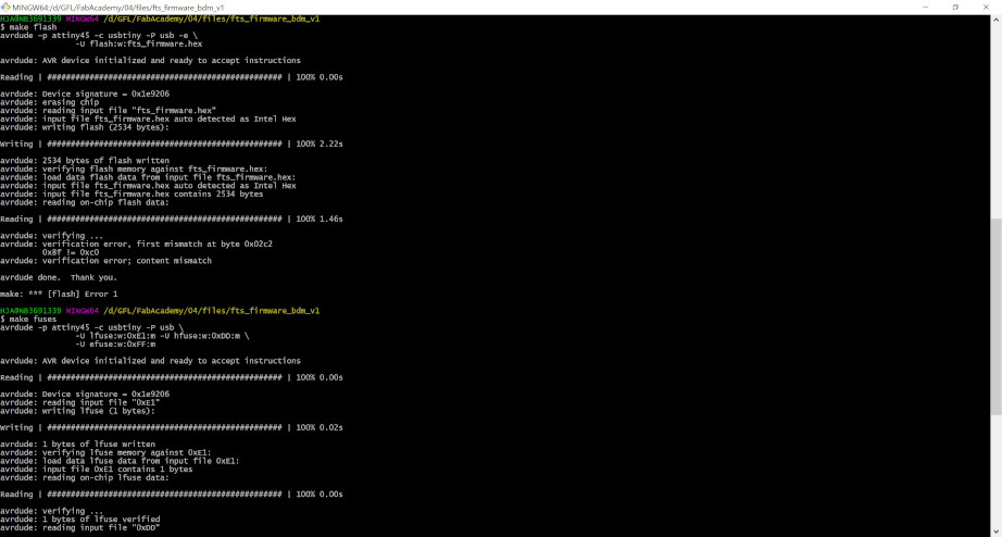
After doing this, the programmer was successfully recognized by my computer’s device manager. The last step was to desolder the bridge.