Week 4: Electronics production
Assignment for this week:
Group assignment: Characterize the design rules for your PCB production process
Individual assignment: make an in-circuit programmer by milling and stuffing the PCB,
test it, then optionally try other PCB processes
- Introduction
This week I’ve learned a lot about electronic components and their usage from the different aspects. I have a background in physics, but in materials I found way more information about the same components, which I used differently. I made a PCB board by milling and soldering the components, programmed and tested it.
Here are some documentation, which were helpful for me. I started from this tutorial, then following links there I have found these ones: - Test soldering
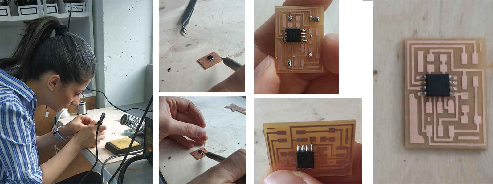
In the lab our instructor explained one more time how to do proper soldering and desoldering, best practices, etc. . Then I did some trial ones. It seemed complicated in the beginning, but I got used to it pretty fast. I found this tutorial, which helped me a lot for doing good soldering.
Preparing the Soldering Iron: Tinning the Tip
- Place the soldering iron in its stand and plug it in.
- Wait for the soldering iron to heat up.
- Moisten the sponge.
- Wipe the tip of the iron on the damp sponge. This will clean the tip.
- Melt a little solder on the tip of the iron.
- This is called tinning and it will help the heat flow from the iron's tip to the joint.
- The solder should flow onto the tip, producing a bright shiny surface.
- If the solder will not flow onto the tip, clean it by wiping it on the wet sponge.
- When tinned, wipe excess solder off on the wet sponge.
- You do not need to tin the tip before every joint, but you should re-tin it if it has gone dull when the soldering iron has not been used for a few minutes.
- Check the manufacturer's instructions related to tinning the tip.
- The tip of the soldering iron should be a shiny silver color. If it is black and pitted, replace it with a new one.
Soldering
- Solder needs a clean surface on which to adhere.
- Buff the copper foil of a PC board with steel wool before soldering.
- Remove any oil, paint, wax, etc. with a solvent, steel wool, or fine sandpaper.
- To solder, heat the connection with the tip of the soldering iron for a few seconds, then apply the solder.
- Heat the connection, not the solder.
- Hold the soldering iron like a pen, near the base of the handle.
- Both parts that are being soldered have to be hot to form a good connection.
- Keep the soldering tip on the connection as the solder is applied.
- Solder will flow into and around well-heated connections
- Use just enough solder to form a strong connection.
- Remove the tip from the connection as soon as the solder has flowed where you want it to be. Remove the solder, then the iron.
- Don't move the connection while the solder is cooling.
- Don't overheat the connection, as this might damage the electrical component you are soldering.
- Transistors and some other components can be damaged by heat when soldering. A crocodile clip can be used as a heat sink to protect these components.Soldering a connection should take just a few seconds.
- If it is taking longer, see the troubleshooting section below. Inspect the joint closely. It should look shiny.
- If you are soldering a wire (called the lead) onto a PC board (on the track), it should have a volcano shape
- If the connection looks bad, reheat it and try again.
- Unplug the soldering iron when it is not in use.
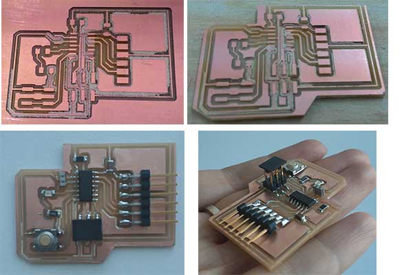
- PCB fabrication
After doing trial soldering, we had some explanation in a group about PCBs, what is that for, components, what do they do, etc.
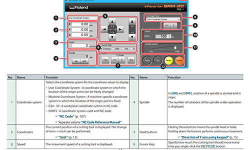
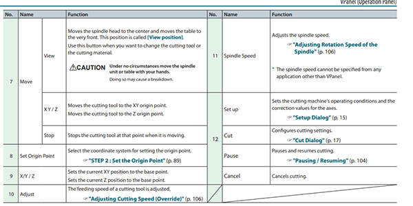
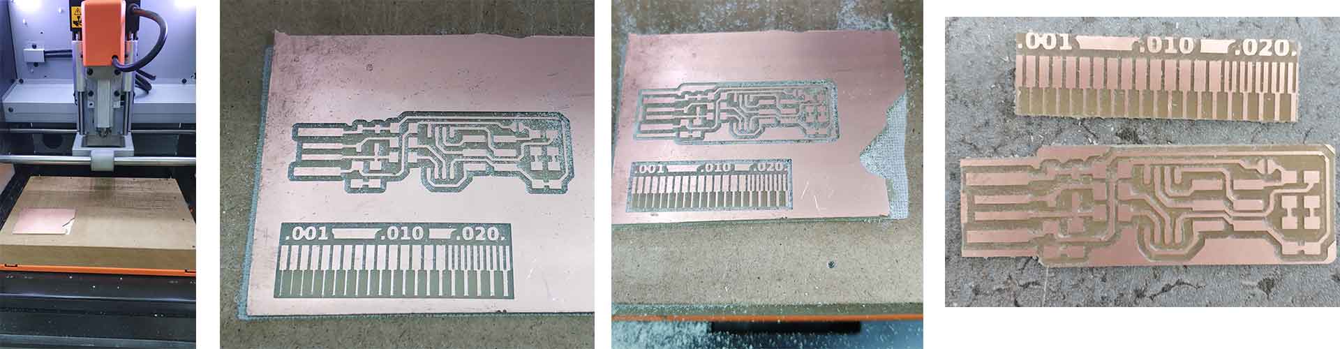
To not waste the time and material, I decided to cut both line test and PCB base on the same material. Line test is for testing the machine and finding out the thickness of the line, which can’t be cut out, the tool can’t enter and cut there. For that I did following steps:- READ the machine user manual , how it works the safety rules, etc. The basic functions on the mains screen are described here.
- Using two sided tape, attach the material to the machine table. As it should be tightly attached, I put that under the pressure for some time.
- Download the following .png files
Traces for linetest
Interior for linetest
Traces for PCB
Interior for PCB - Go to fabmodules.org and follow these steps. First we are going to cut traces both for line test and PCB. For that in “process” part we have to choose PCB traces (1/64), because i’m going to use 1/64 end mill.
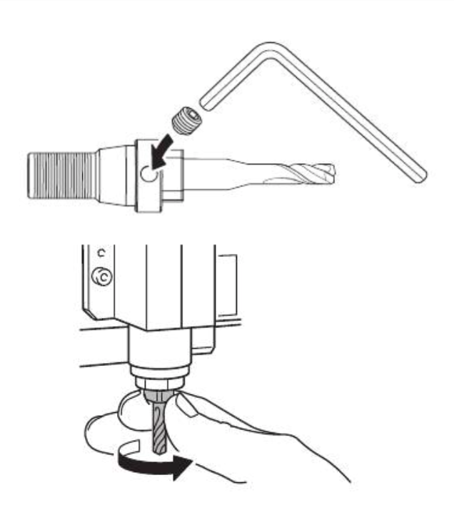
- Carefully attach the cutting tool to the machine as it shows in the manual. For that:
-
Insert a cutting tool in a collet. Do not insert to the portion of an edge. When you use included cutting tool,refer to the following figure.
- Tighten the set screw with hexagonal wrench.
- Loosely tighten the collet with cutting tool
- Fully tighten the collet.
-
Loosen the set screw with hexagonal wrench. Support lightly by hand not to drop a cutting tool.
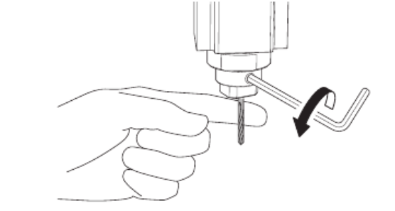
- Remove the cutting tool.
- Attach the cutting tool which you want to use ,and tighten the setscrew
-
Insert a cutting tool in a collet. Do not insert to the portion of an edge. When you use included cutting tool,refer to the following figure.
- Using the tools in the main screen on the programm, set the position of the tool in the place, when you want to start cutting and set X/Y/Z axises as 0 for G54 coordinate system. You can find more about G coordinate systems here.
- As I was going to cut two models on the same board, I used G54 and G55 systems.
- When cutting is finished, I did the same thing for the interiors of the line test and PCB base. For that I used 1/32 end mill.
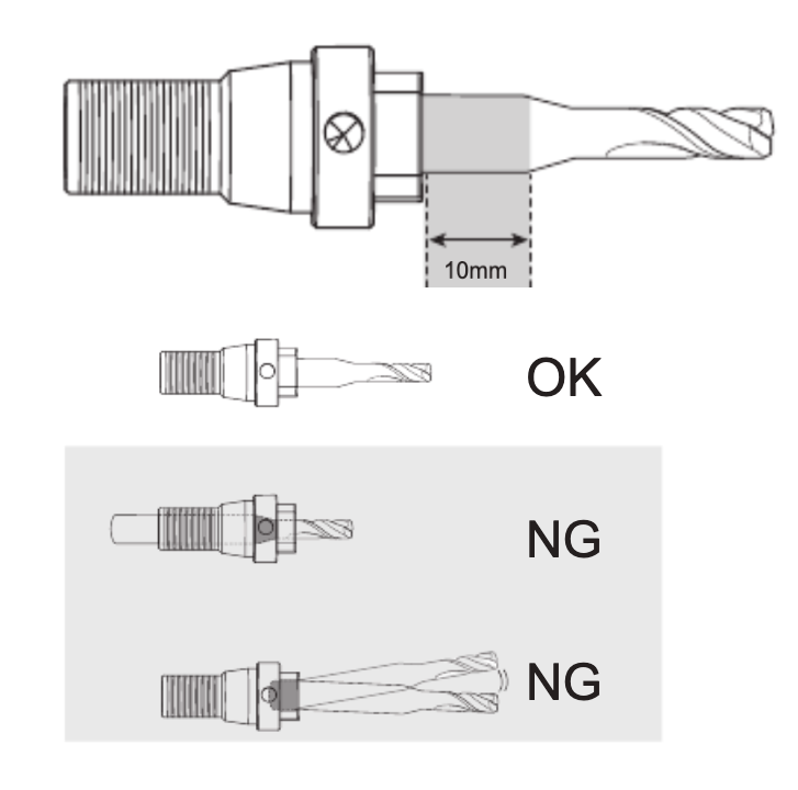
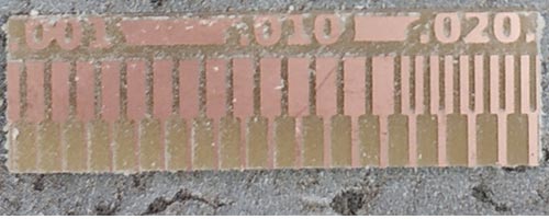
- Check the results. According to the results of my line test, 1/64 end mill is not able to cut lines less than 0.15mm.
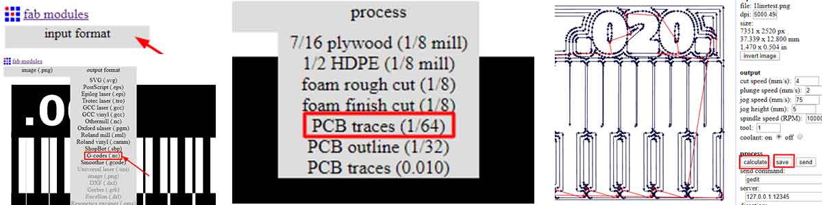
Here are the files I used for milling and cutting
Linetest
Linetest interior
PCB traces
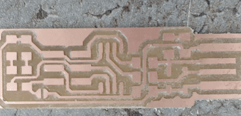
PCB interior - Assembling the PCB
After having the PCB base ready, I started to assemble the components. We need following ones:- 1x ATtiny45
- 2x 1kΩ resistors
- 2x 499Ω resistors
- 2x 49Ω resistors
- 2x 3.3v zener diodes
- 1x red LED
- 1x green LED
- 1x 100nF capacitor
- 1x 2x3 pin header
- Programming ATtiny45 and testing
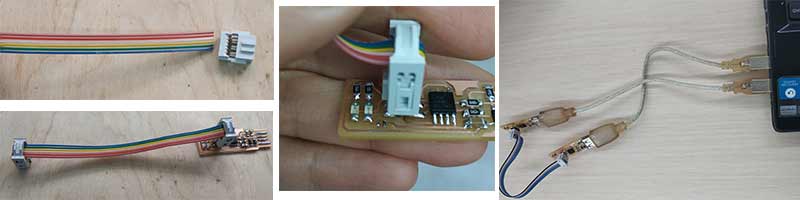
After soldering all the parts, I did programming following the steps in Brien’s documentation. As a programmer I used the ICP made by my instructor Babken last year.
- Install Avrdude. For Ubuntu , enter the following command, followed by your password when prompted:
sudo apt install avrdude gcc-avr avr-libc make - Download the firmware source code and extract the zip file. Open your terminal program and cd into the source code directory.
- Run
make.This will build the hex file that will get programmed onto the ATtiny45. When the command completes, you should now have a file called fts_firmware.hex. - I did't update the Makefile because by default it assumes that you're going to use a programmer in the usbtiny family
- Connect the programmer to the ISP header on the board and then using USB extension cable, connect to the USB port.
- Run
make flash.
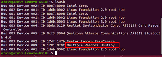
You should see several progress bars while avrdude erases, programs, and verifies the chip. - Run
lsusb. If everything is done properly, you will see "Multiple Vendors USBtiny" in command line - Run the
make fusescommand.
 To have a programmer board from my one, I had to do following steps:
- Connect my ISP programmer to your board one more time, and run make
rstdisbl.
This does the same thing as the make fuses command, but this time it's going to include that reset disable bit as well. You should see some progress bars, and with that, avrdude will never be able to talk to this chip again through the ISP header. - We need to disconnect VCC from the Vprog pin on the ISP header by removing the bridge on the solder jumper.
- Install Avrdude. For Ubuntu , enter the following command, followed by your password when prompted:
-
Conclusion
This was a very productive week for me. Even though I don’t completely understand how PCBs are designed and why we have components in places given us, I enjoyed milling and cutting, finding proper components, soldering and desoldering. And of course the most exciting part was the moment, when I realized that my board works. - Files