Week 6: Electronics Design
Assignment for this week:
Group assignment: Use the test equipment in your lab to observe the operation of a microcontroller circuit board
Individual assignment: Redraw an echo hello-world board, add (at least) a button and LED (with current-limiting resistor)
check the design rules, make it, and test it
extra credit: simulate it's operation
- Introduction
This week was full of new experience, interesting learning outcomes, failing, troubleshooting and fixing. It was very complicated to design the board, but once I got the basics, it became easier. worked in KiCAD for the first time and liked the process a lot. Here are some useful links to start with, if you are new in KiCAD as me:
KiCAD PCB Design Tutorial
-
Kicad vs Eagle
The first thing I had to do for designing the PCB is choosing the platform. I had to choose between KiCAD and EAGLE . I started to read articles to compare them. For me essential things for choosing the platform are the price and user-friendliness. Following articles are very useful if you didn’t use neither of the platforms and want to choose one:
PCB design: Eagle vs KiCad – the verdict
Kicad vs Eagle - Which one is best?
Even though the Fab Academy tutorials page I found resources only for Eagle, after reading these articles, I decided to use KiCAD for several reasons:- Price: KiCAD is a free open source program and works for all of the OSs. EAGLE is an Autodesk product and has some limitations for non-paid options. EAGLE is only available with a Fusion 360 subscription. Furthermore, you can't have more than 2 schematic sheets, 2 signal or plane layers, 80 cm2 (12.4 in2) board area. For now, I won’t need more than this, but I never know what will happen in future.
- Existence of hotkeys: In KiCAD there are default key shortcuts, which are very helpful. You can have hotkeys in EAGLE as well, but for that you have to set them up
- Default 3D viewer. This is a very useful tool, if you want to get a good understanding of size and space. It’s hard to do so in the board designer part for me, so 3D viewer was a huge bonus.
- Designing the schematic
- To start designing the schematic, open KiCAD, go to File → New project. Choose the location of the folder and name the folder. Then go to the schematic editor ( Echoschema ).
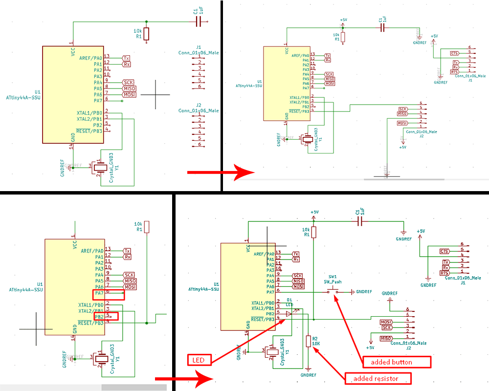
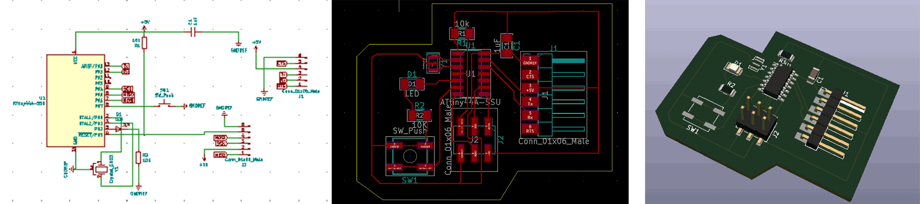
- Click on the Place Component icon in the right toolbar and find components that you need from the library. To move the component you can hover it and press M , to rotate R and to change the value V. You can also duplicate a component already on your schematic sheet by hovering over it and pressing the C key. Click where you want to place the new duplicated component. Those hotkeys are very useful. I added the components which are there on Neils board.
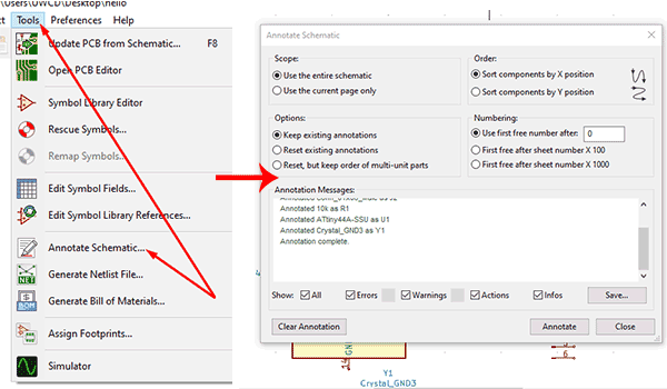
- When you have all of your components ready, go to the top toolbar, choose Tools → Annotate, this will annotate the components and it will be easier to differentiate them.
- Connect the pins. This article was very helpful for understanding best practices in connecting and wiring. I assigned global labels, chose the wiring icon and started to connect pins to each other. The ones, which have global labels will be connected automatically.
-
I added a button and a LED with 10kOm resistor to the Neil’s board. I had pins 5 (PB2) and 6 (PA7) free on my ATtiny44, so connected LED to 5 and button to 6 . We have to add a resistor to LED in series. Such a resistor is often called a ballast resistor. The ballast resistor is used to limit the current through the LED and to prevent that it burns.If the voltage source is equal to the voltage drop of the LED, no resistor is required. Read more here.
In summary I have the following components:- ATtiny44 microcontroller
- 6-pin programming header
- FTDI header
- 20MHz resonator
- 1uF Capacitor
- 10k ohms Resistor *2
- 499 ohms Resistor
- Button
- LED
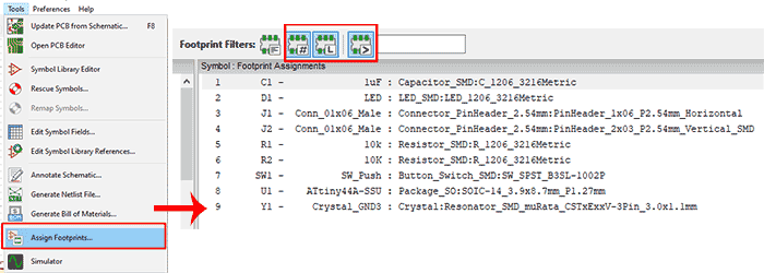
- Go to Tools → Assign footprints . Here you have to choose footprints for your components and you are done with the schematic.
-
Click on Perform electric rules check
 icon to see whether you have everything connected or there are some errors.
-
Go to Generate netlist
 icon. This will generate the netlist, which will be used in PCB designer file.
- Designing, printing and cutting the PCB
- Go to Tools → Layout Printed Circuit Board
- The opened window will be empty yet. Go to Read Netlist icon, click it and ask to read your generated netlist. All the components with their footprints will be placed on the board and pads are connected to each other with white lines.
- The hardest part for me was placing the components in the proper positions and do routing (connecting footprints by wires). In the beginning I had some problems with placing and routing. I tried several ways of placing, but always ended up having a jungle - style board.
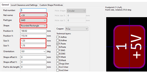
- Eventually, I started to compare my board’s layout with Neil’s one and found out that I had put different orders for the footprint. To change the footprint manually double click or right click on it and choose Properties. Here you can change the name, style, size of the footprint.
- When I had the proper order of footprints for all the components, wiring and routing was not that complicated.
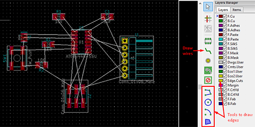
- To connect the components click Add tracks and vias on the right toolbar or press W on the keyboard. Then start connecting the components. Here as well you can move and rotate the component to have a better layout and connect them easier. Also, there is a possibility to draw wires on the front or on the back side of the board. For that in the layer selection part select F.Cu for the front or B.Cu for the back.
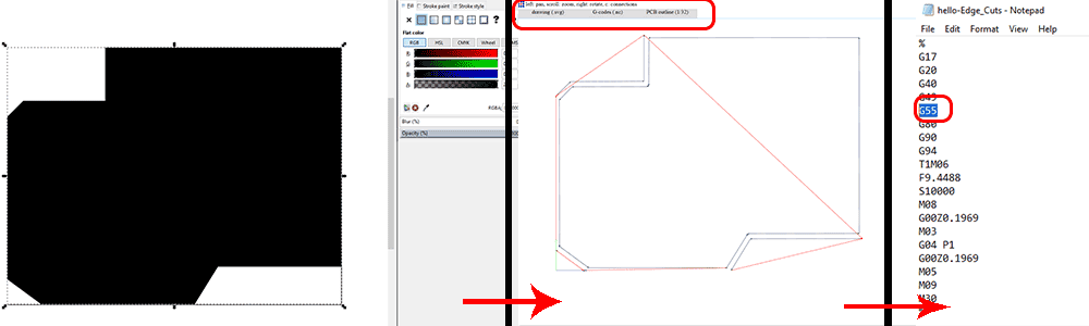
- After spending plenty of time for the routing, I had the ready board. I chose the Edge.Cuts layer on the right toolbar and drew the outline of the board. There are some simple tools, which you can use to draw the edges.
- Go to the View → 3D viewer and see if you are satisfied with the layout, placement, sizes and the view. If so, the PCB is ready to be manufactured.
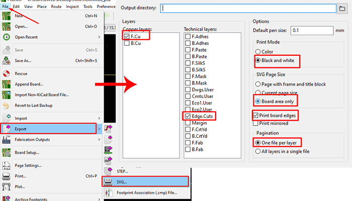
- Go to File → Export → SVG and select the following settings to have drawings of all the layers.
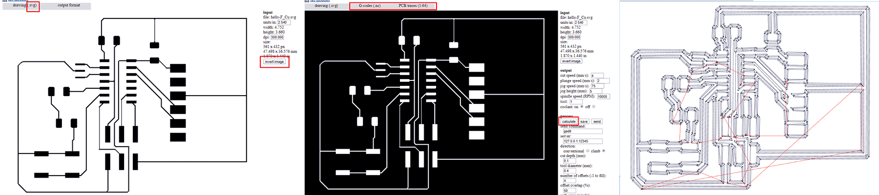
- To have the printable version of the designed PCB go to Fabmodules.org and follow the same procedure as in Week 4. I had 2 files to process: one for traces and the outline.
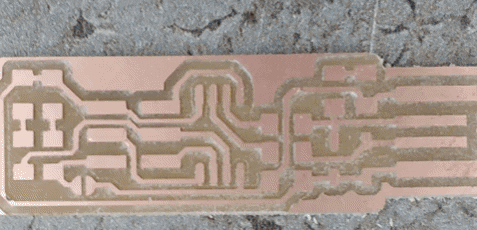
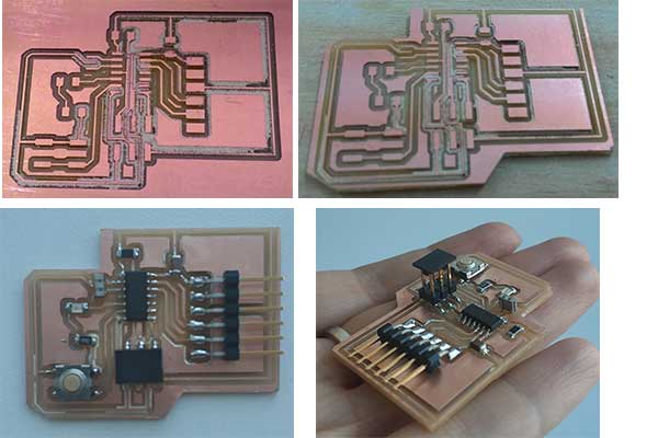
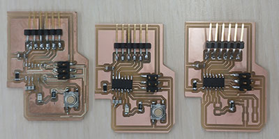
- Here is the board after cutting and soldering. The edges are very closed to the traces, so next time I will consider it and draw the edges further.
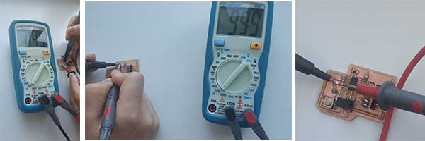
- After having the ready PCB I did some basic electronic tests on it and here are the results.
-
Programming the board
For programming the board I went to the Fab Academy Embedded programming week lesson’s page, downloaded echo.c and echo.c.make files for ATtiny44 and put them in one folder. Also I have downloaded the term.py file from Input devices week’s lesson page.
As I didn’t have Python installed on my computer, first of all I installed it running the following command in Terminal.
sudo apt install python
After successful installation I opened the folder with downloaded code files, ran the terminal there and started programming by following the Fab Academy tutorial.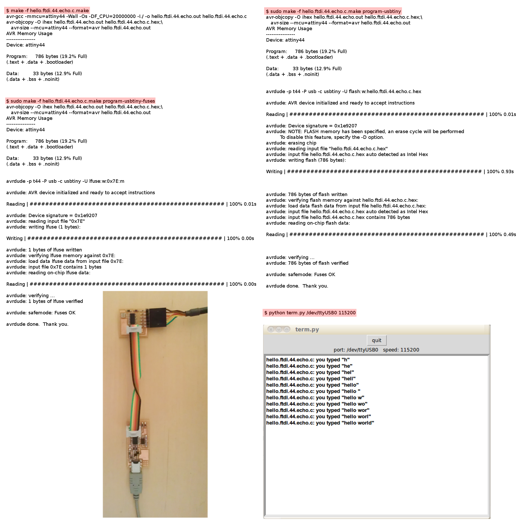
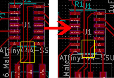
I got an error there and while checking the board with my instructor Babken we found out that 2 traces which should be separated are connected, because I have designed them too close to each other and the endmill couldn’t go there.
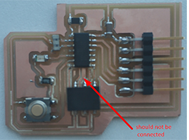
I changed the design, moved traces further from each other and cut the second board. After assembling it I have tried to program it once more.
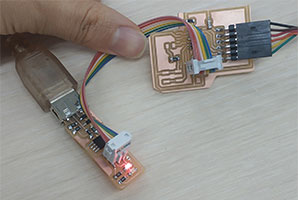
I connected the board to my Fab ISP and to the computer via FTDI cable. Fab ISP is connected to the computer USB.
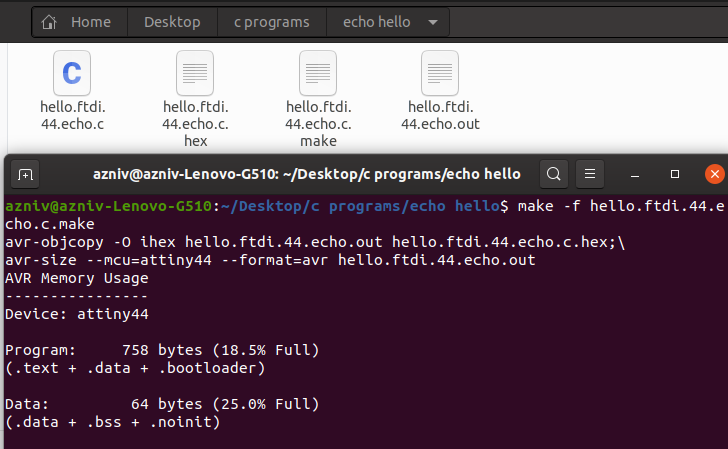
I opened the terminal in the folder with the codes and run the following commands-
ls /dev
In the opened list we should have tinyUSB0 -
make -f hello.ftdi.44.echo.c.make
Here I got this
-
sudo make -f hello.ftdi.44.echo.c.make program-usbtiny
On this line I got the following error.
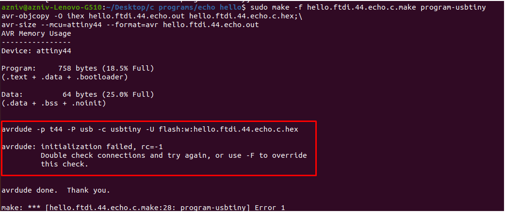
I have tried different combinations of connections and it still didn’t work. I checked all of the connections with the digital multimeter and didn’t find anything which could cause the error. I have compared the design with Neil’s board as well and again, everything seems similar. So my only doubt was in the process of soldering. I was thinking that maybe I’ve destroyed the microcontroller during the soldering.
So I cut and more carefully assembled the third board as well, which again didn’t respond on the same command. Me and my instructor checked all the possible things and couldn’t find the reason.
-
-
Conclusion
This week was very challenging and sometimes stressful, but the learning outcome was worth it. I have learnt how to design a PCB, which components do we need and why, how to assign proper footprints, how to prepare design for the milling and how to assemble the board properly. I enjoyed the research, working on KiCad, even the failing and trying again. When something doesn’t work from the first trial, that makes me to do more research, go more deep into details and learn more.
I was stressed when I could not program the board, but this has an advantage as well: after assembling three boards I know by heart all the traces and components of my board.
- Files
Press here to download original files.