Electronics Production
Week 8 · 🔧 PCB milling & soldering
📋 Assignment Overview
⚡ Week 8 documents Electronics Production: fabricating a PCB, soldering, and testing. Below is the workflow from design export through production.
📋 Assignment Process
🖥️ Software used
Pre-export: Autodesk Fusion 360
Machining (Windows lab PC): Roland MDX-40 Panel, ModelA Player 4
Fusion 360 download: https://www.autodesk.com/products/fusion-360/overview
ModelA Player 4 download: https://www.rolanddga.com/support/products/software/modela-player-4 — official Roland DGA page for the Modela Player 4 installer and updater.
Steps below: Pre-export (Fusion) · Machining (Panel + CAM).
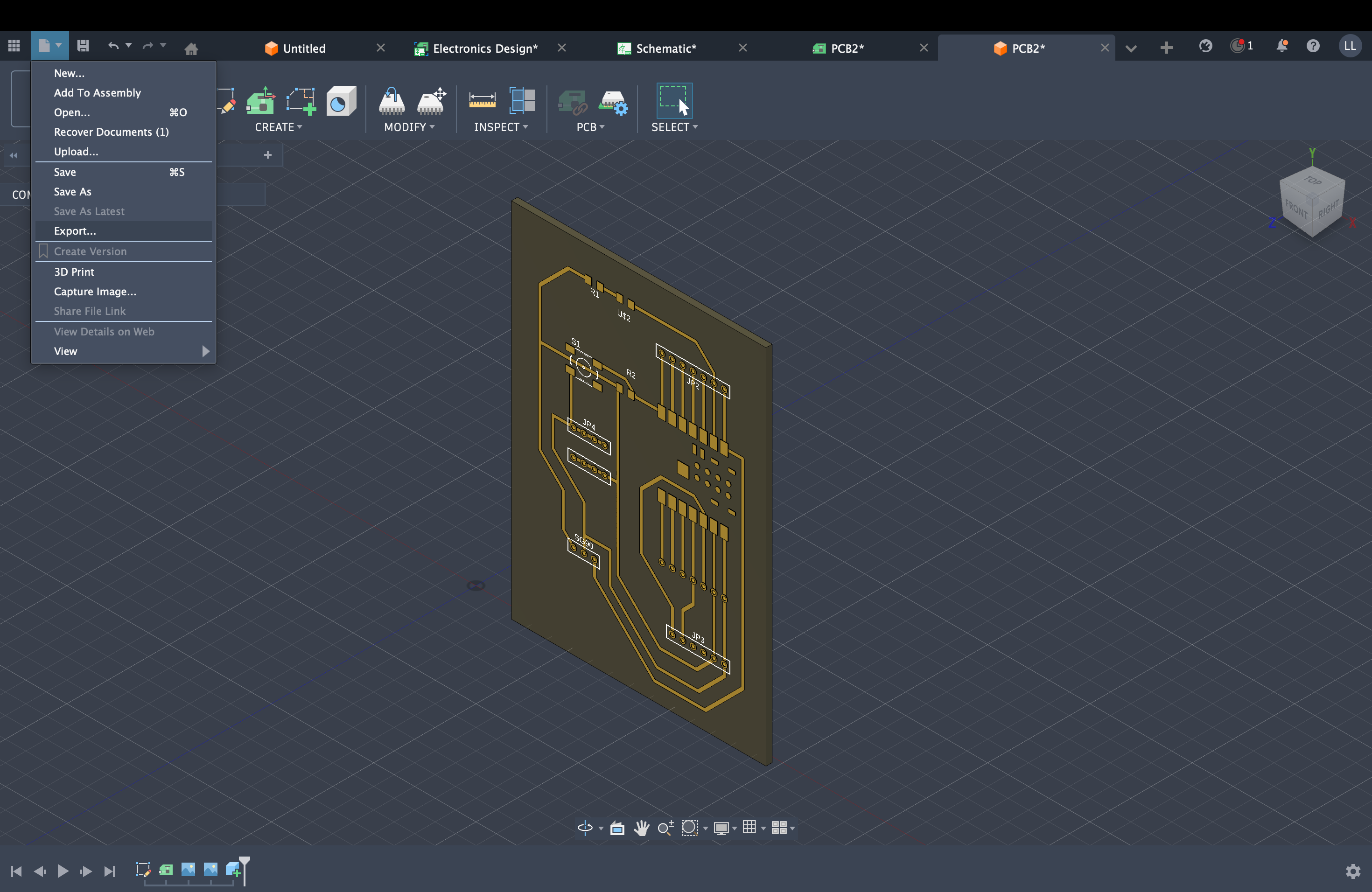
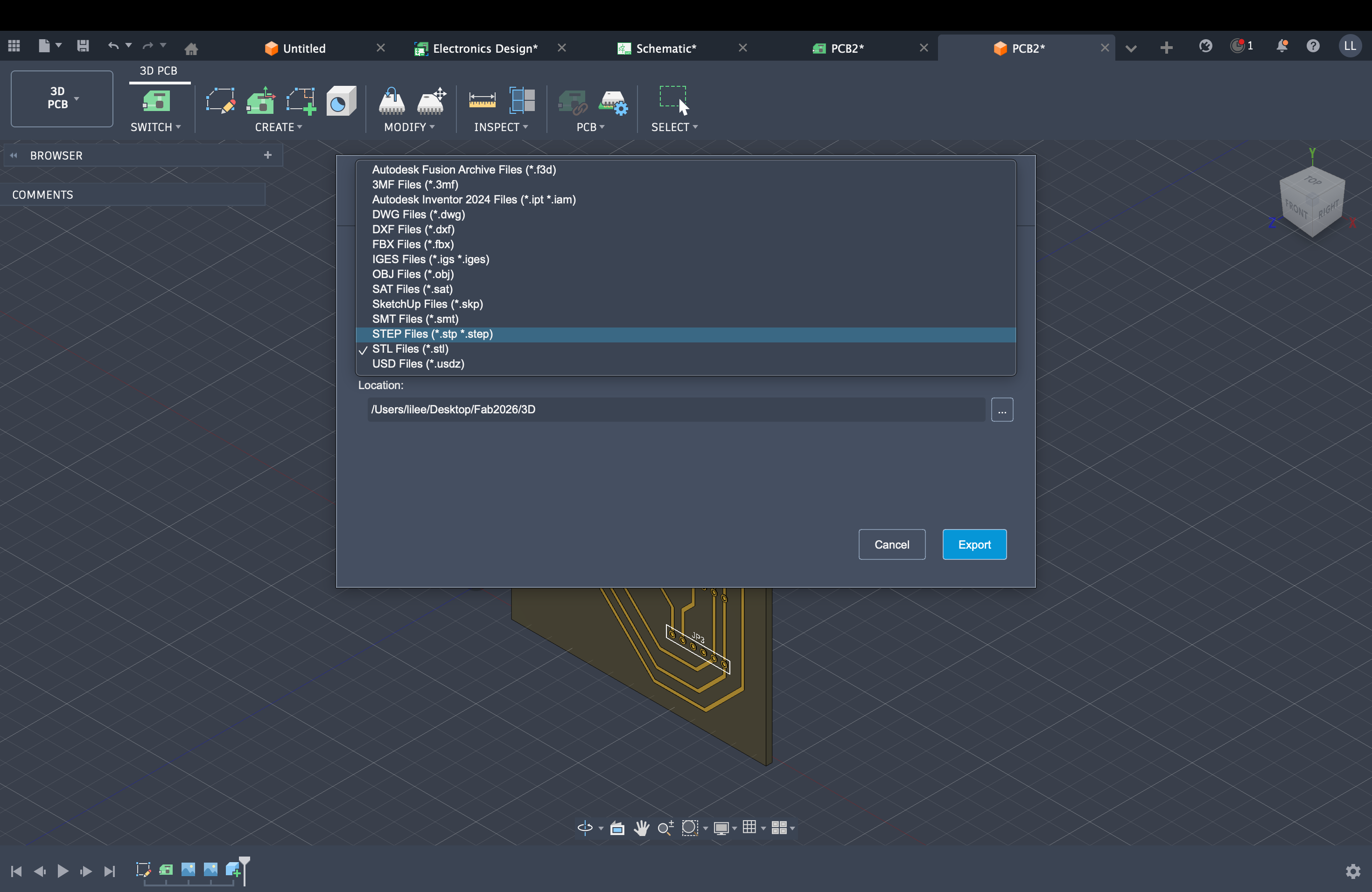
📤 Step 1: Copper layer only — export STEP
After finishing the 3D PCB output, remove the other unnecessary bodies and keep only the copper layer, then export in STEP format.
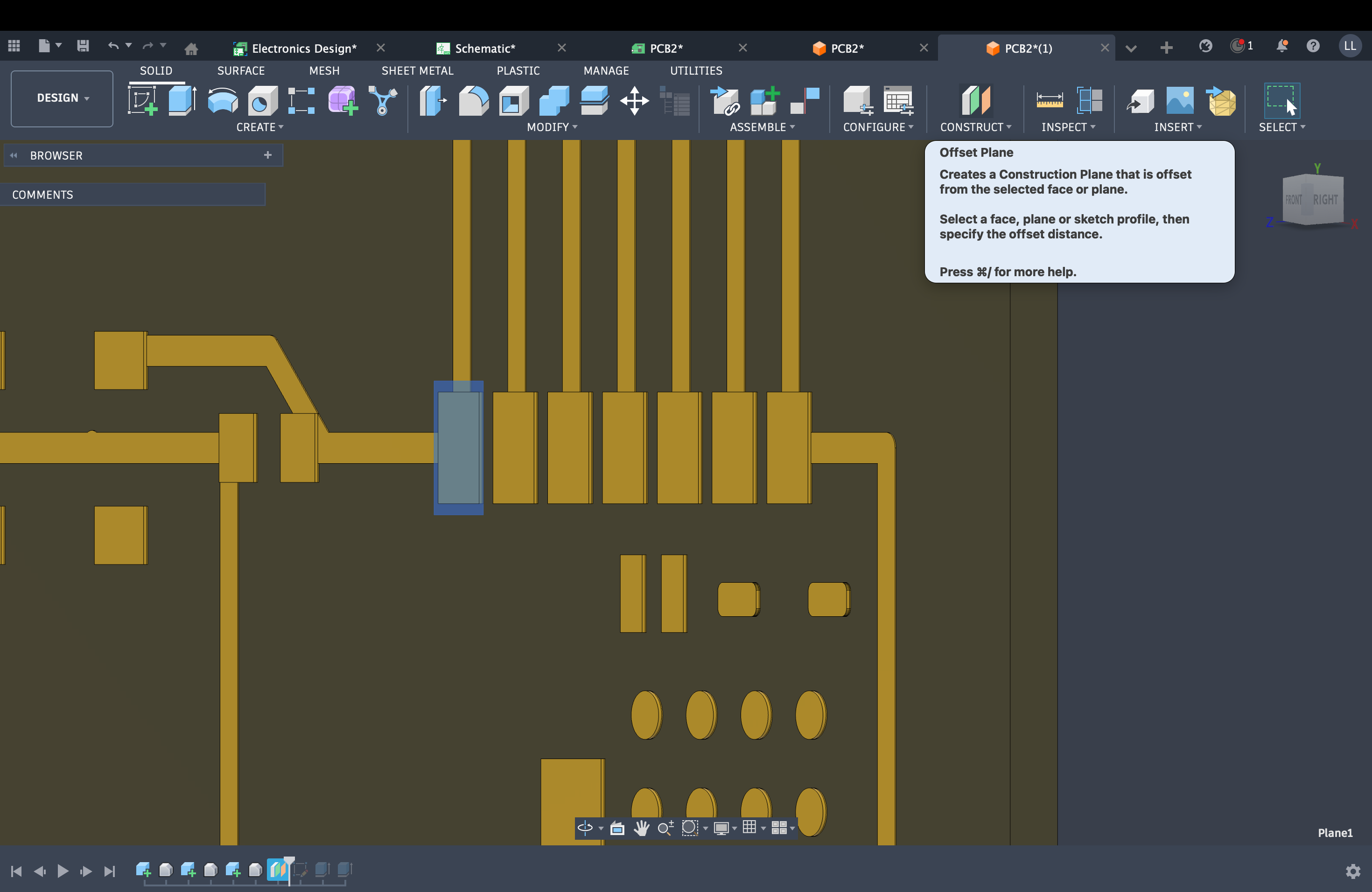
📐 Step 2: Create a face at the top level
At the top level of the design, create a new face (construction surface or sketch plane) as shown.
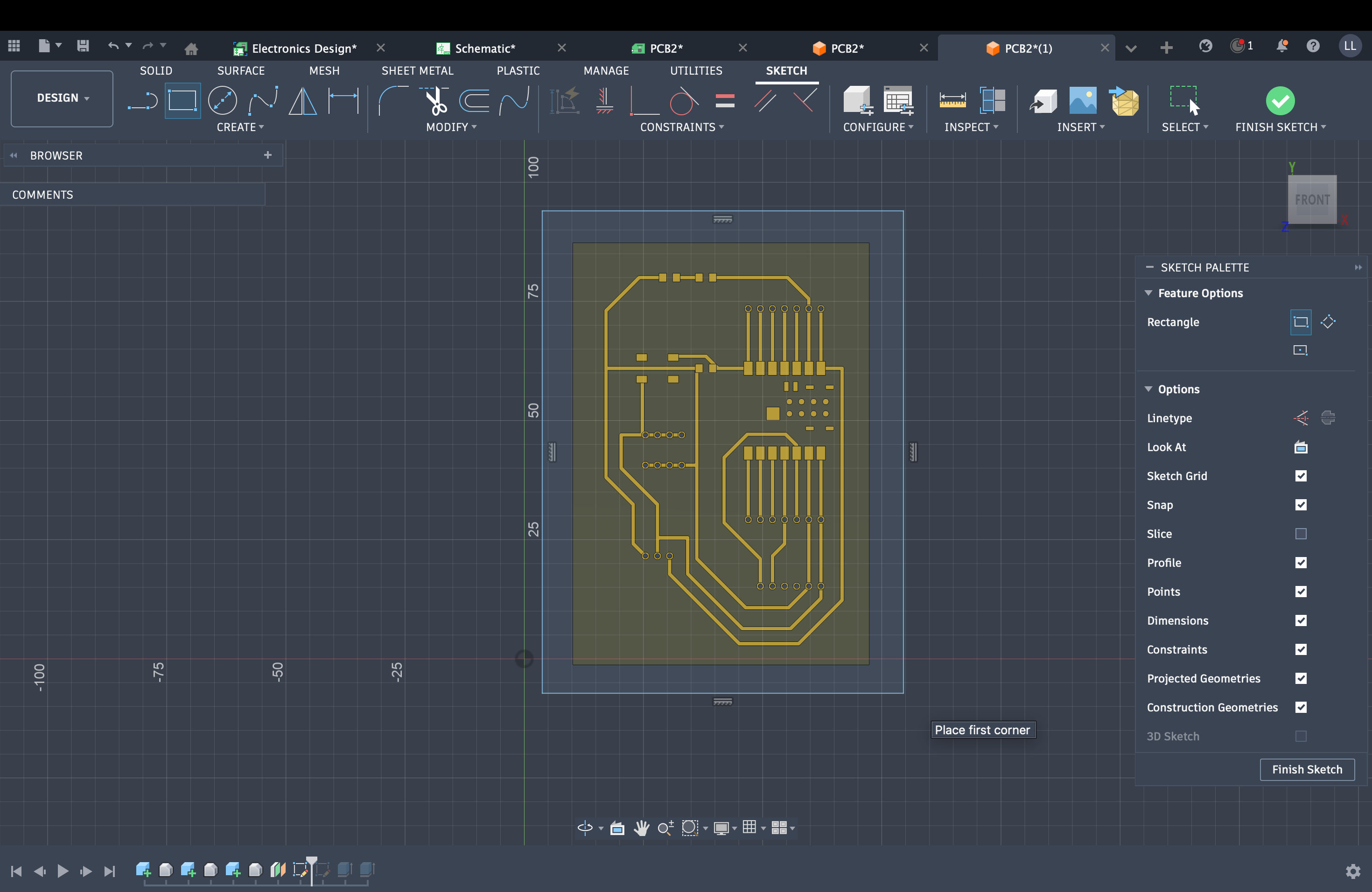
✏️ Step 3: Sketch on the face — level the surface
Create a sketch on that face, then run a facing operation to remove one layer so the top stays flat with no steps or ridges.
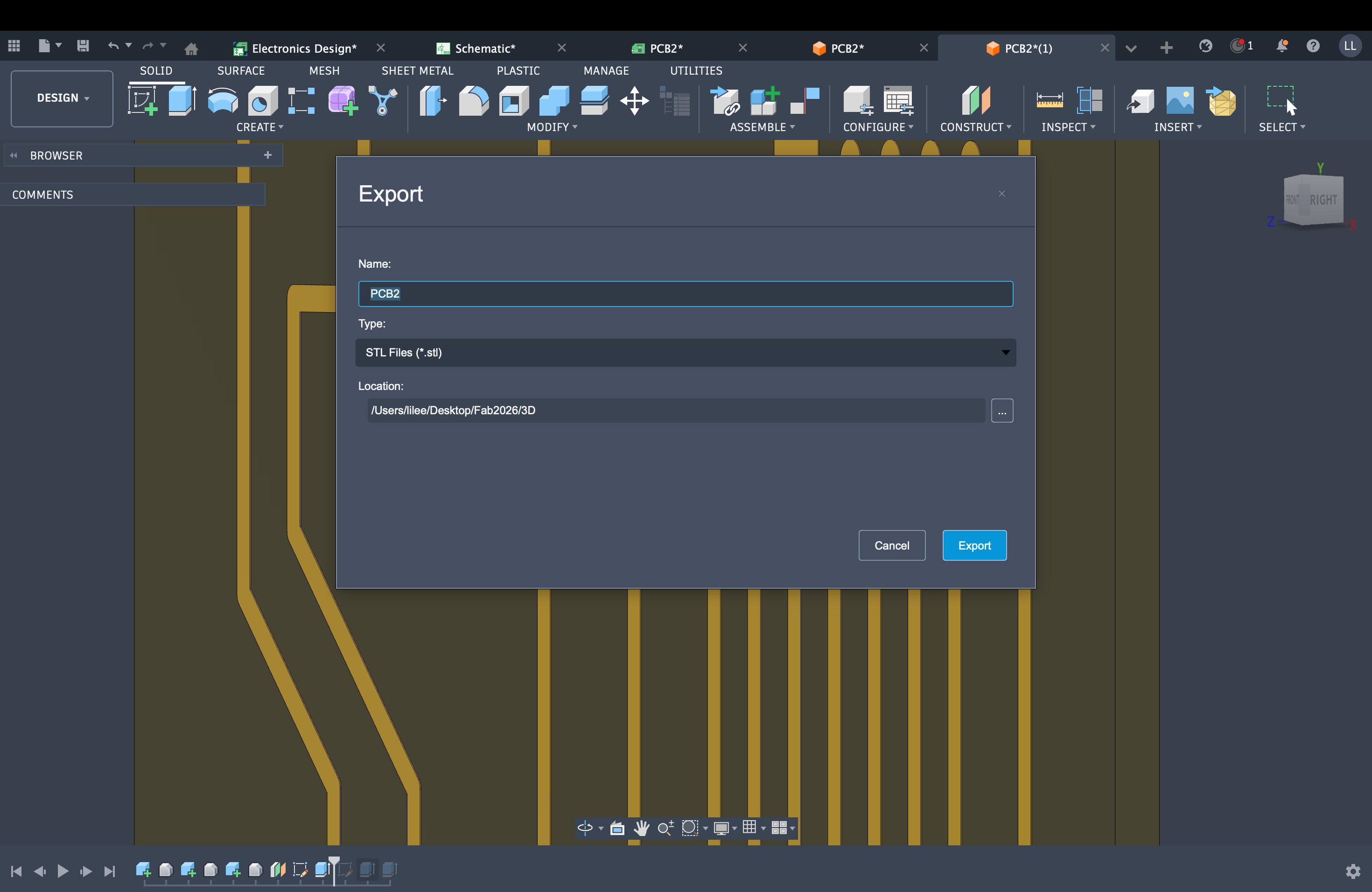
📦 Step 4: Export STL
After facing, export STL from Fusion and set mesh resolution / units as needed.
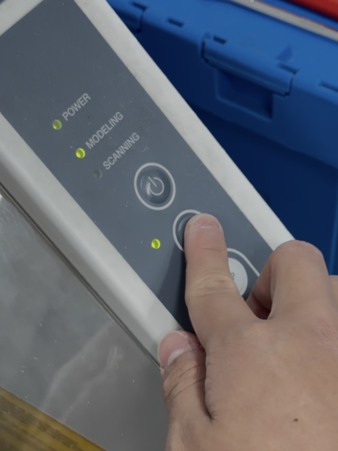
🔌 Step 1: Power on, View, and align the tool
After switching the machine on, click View, then open Roland MDX-40 Panel. Use the software to jog the drill to the top-left corner of the prepared copper board.
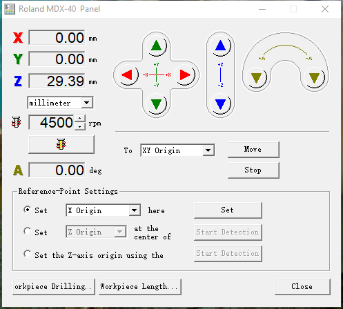
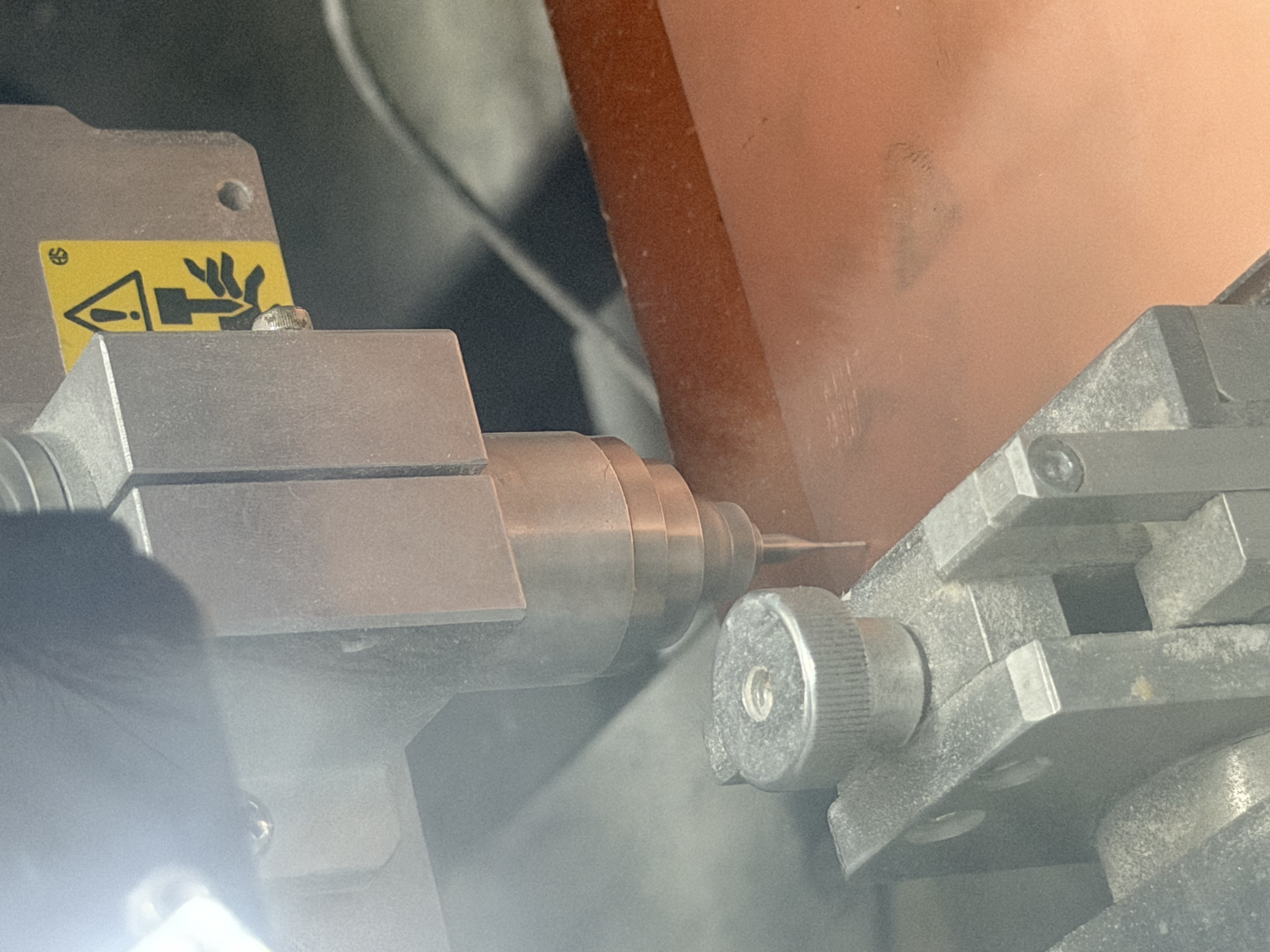
⬇️ Step 2: Spindle on and touch off Z
In the same panel, start spindle rotation, then adjust Z until the bit lightly touches the copper—just a kiss, not deep—to avoid snapping the tool.
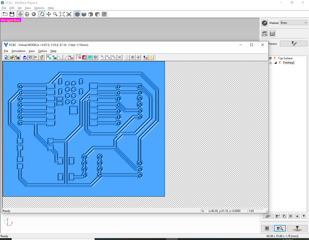
🗂️ Step 3: Machining sequence
From this step on, switch to ModelA Player 4 for CAM and the screenshots below (after setup in Roland MDX-40 Panel in Steps 1–2). Click any thumbnail to view full size. Use the on-screen arrows or keyboard ← / → to move between images. Press Esc to close.
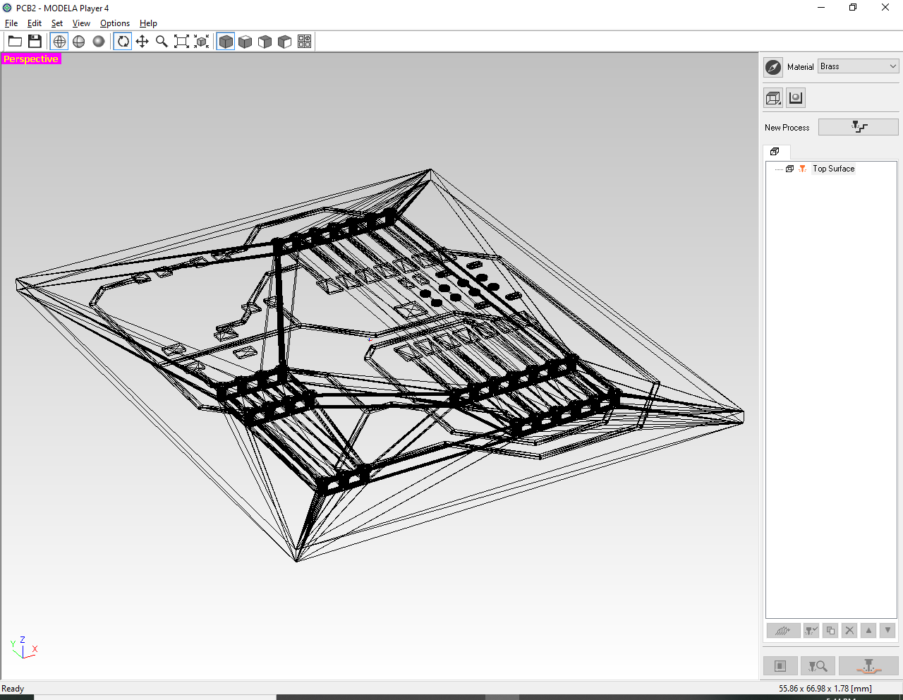
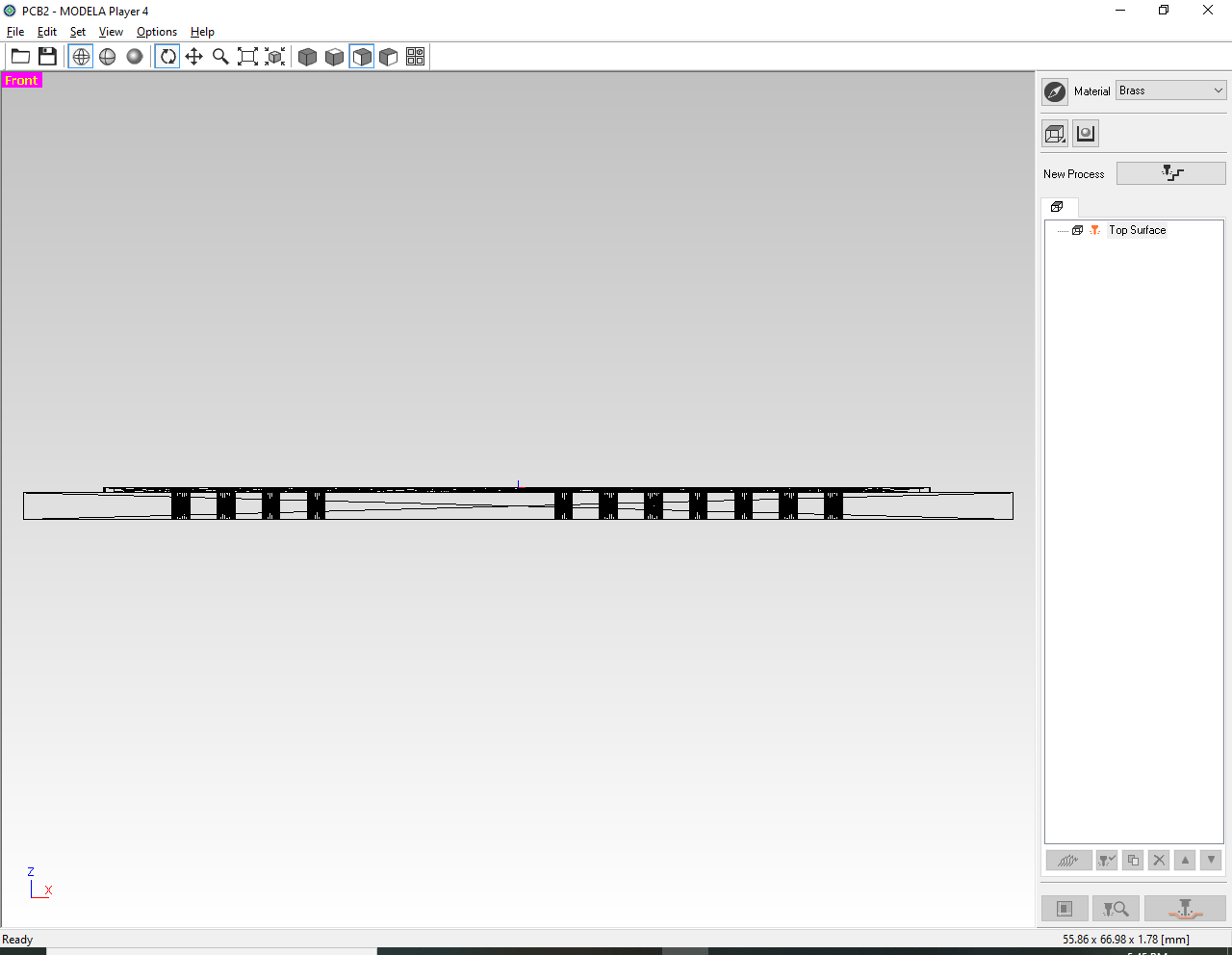
Change the view and verify model thickness.
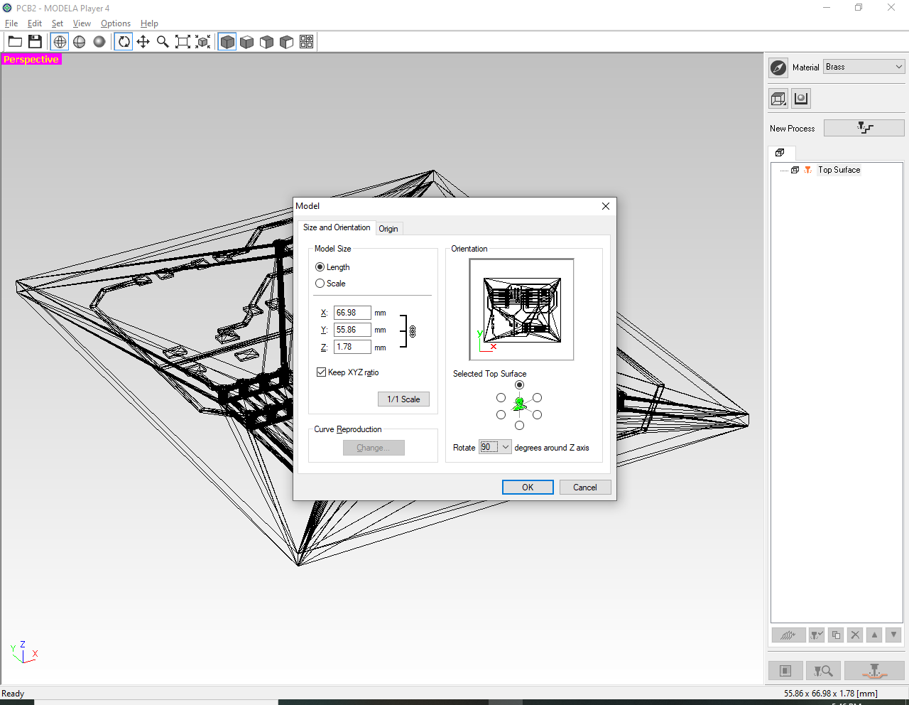
Set → Model size and orientation; rotate 90°.
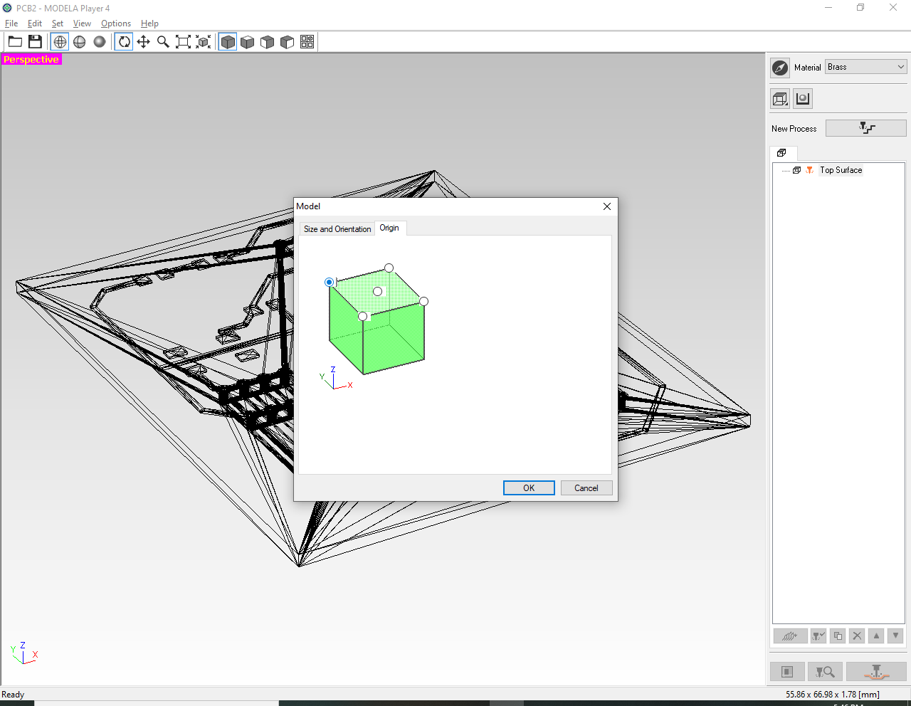
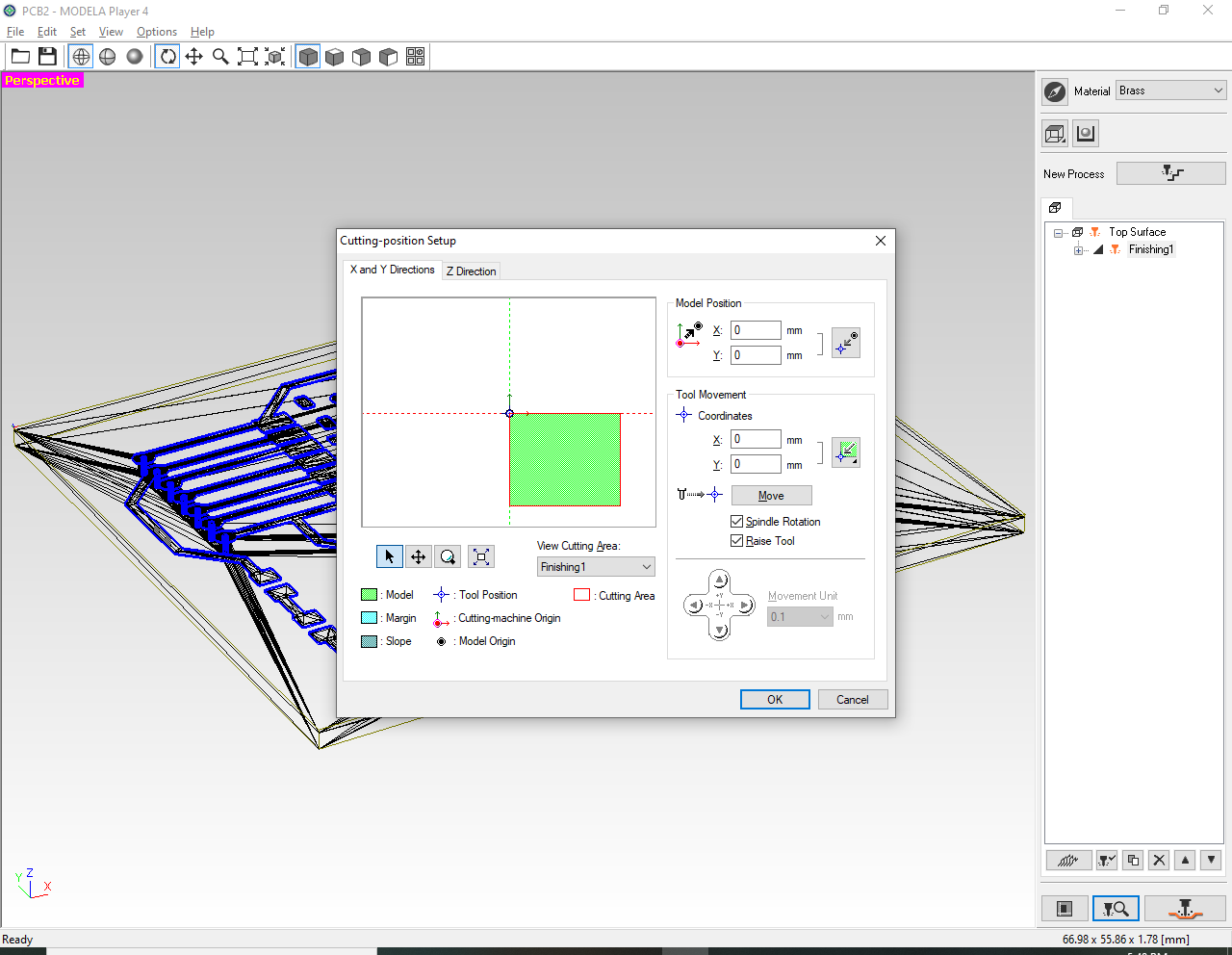
Origin: click the top-left corner as the cut start.
Click New process on the right.
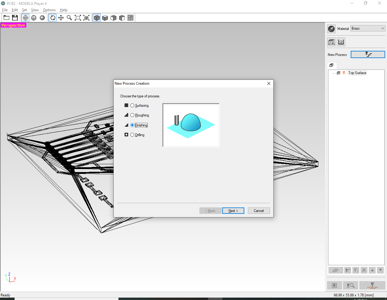
Choose Finishing.
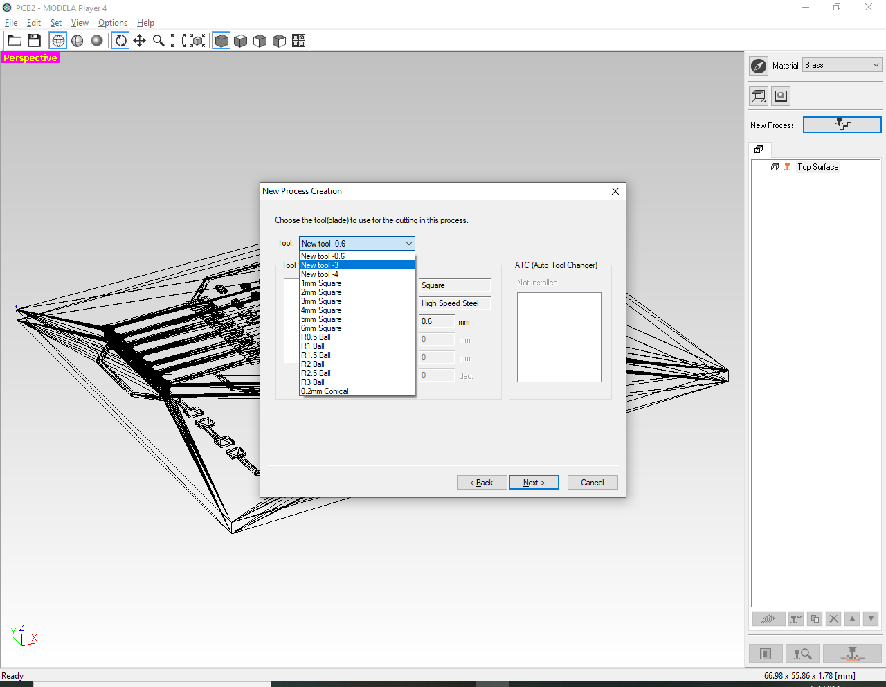
Select your prepared tool / bit data.
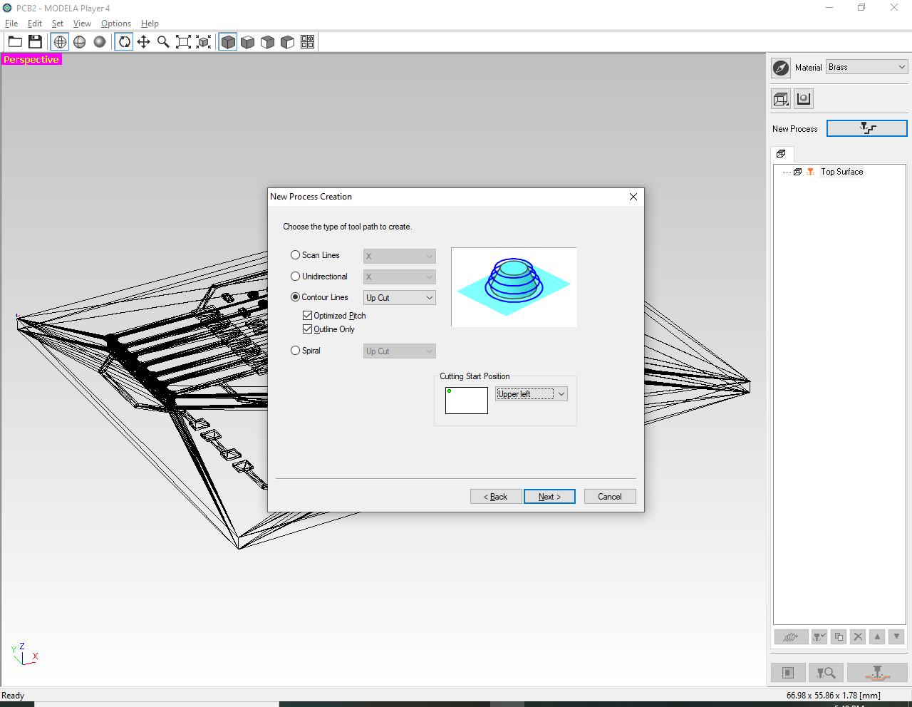
Select Contour lines.
Enable both options below.
▶️ Step 4: Preview toolpath and start cutting
Click Preview in the bottom-right corner to check that the toolpath looks correct. If everything is OK, click Cut (or the equivalent start command) to run the job.
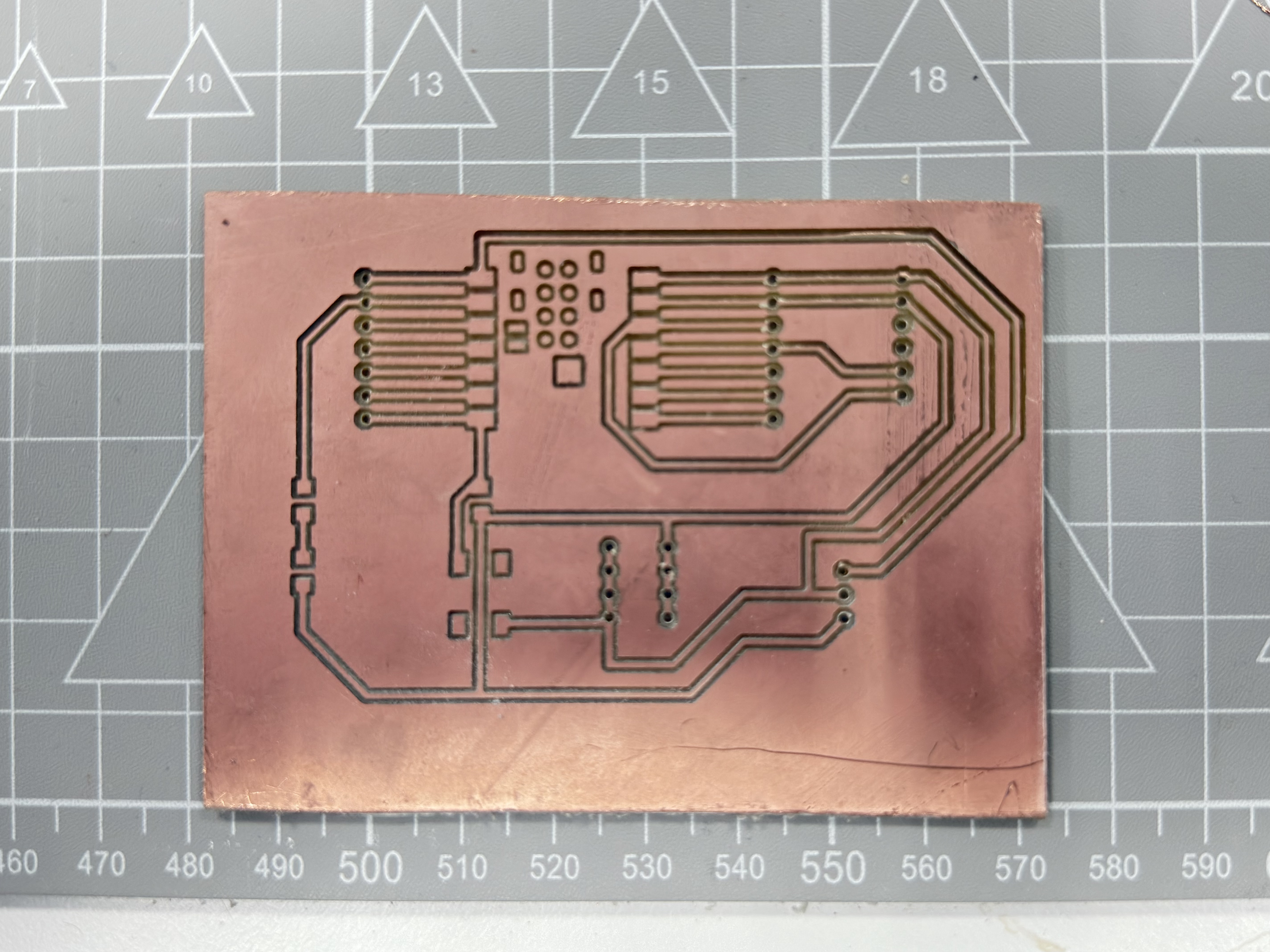
🎬 Step 5: Cutting process
Recording of the machine running the cut, and the milled board after the job is finished.
🔧 PCB design iterations — three revisions compared
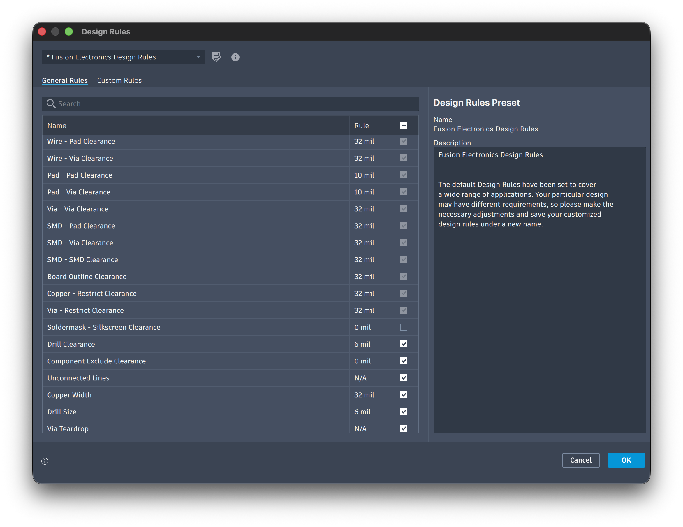
The first milled board failed due to pad and connectivity issues. The table below compares three revisions (V1 → V2 → V3): what went wrong, supporting images, and what we changed each time. The pad issue is resolved in V3; final CAD files are in Week 6 — Final PCB Design (Revision V3).
| Revision | Problem | Images | Solution / next step |
|---|---|---|---|
| V1 — First prototype Initial milled board |
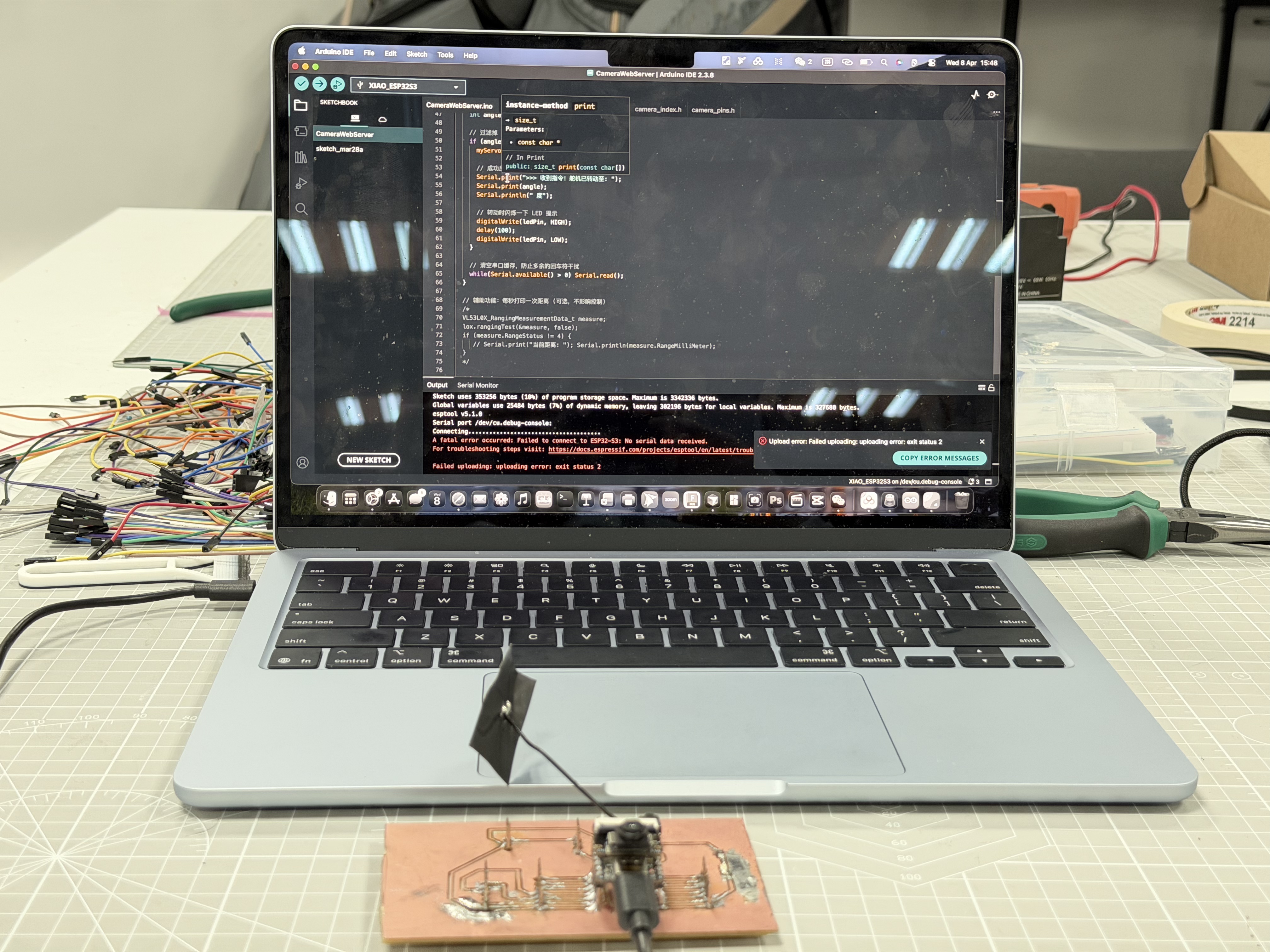
Design Rules (DRC) were misconfigured in Fusion 360. Solder pads were omitted or too weak in the CAM output, causing intermittent connections and poor solder joints. During servo/LED testing, an overcurrent condition damaged the XIAO ESP32-C3. Separately, firmware upload failed: sketch compiled, but esptool reported No serial data received (bootloader/port or damaged module). esptool v5.1.0 A fatal error occurred: Failed to connect to ESP32-C3: No serial data received. |
|
|
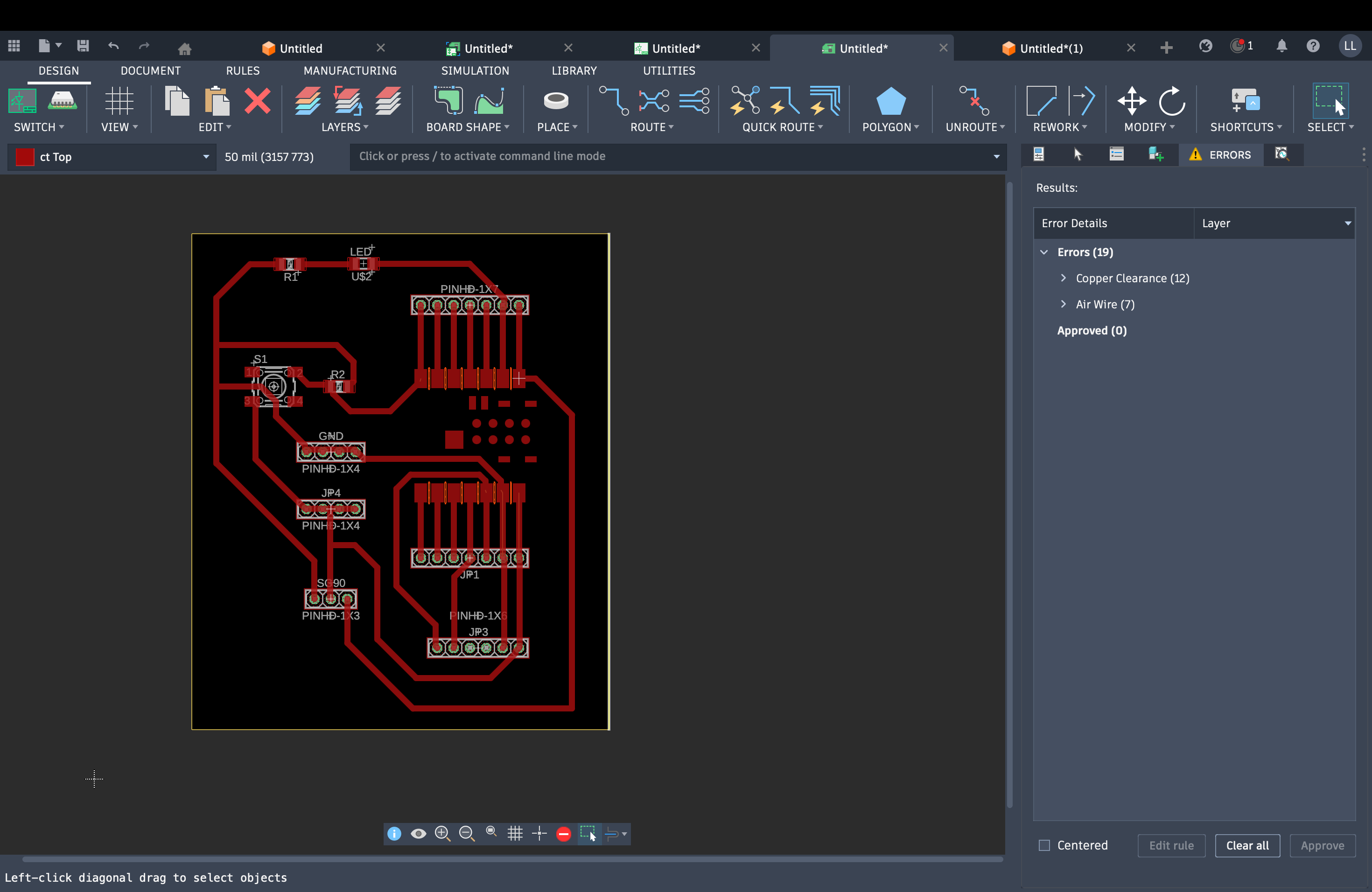
| V2 — DRC-only fix Attempted revision |
Updated Design Rules (DRC) and re-exported the layout. This improved some settings but did not fully solve assembly: pads remained marginal for hand soldering on a single-sided milled board, and mechanical connection was still unreliable. |
|
|
| V3 — Pin headers Final (resolved) |
Small or omitted pads on milled copper were hard to solder and debug. Needed larger, repeatable connection points for modules and wires. |

|
Status: resolved (V3) |