8. Electronics Production
The design guidelines for PCB fabrication using the milling technique and placing an order for a PCB board were the main focus of group effort.
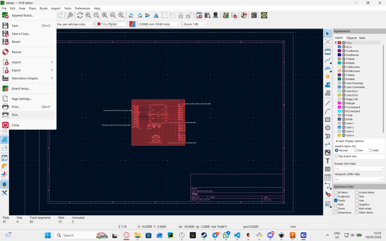
I built and tested the board I created in Week 06 for the individual project. It has a ground plane, 0.5 mm traces, connections, an LED for output, a push button for input, and a Seeed XIAO module. I soldered the parts, machined the board on the LPKF machine, and checked for basic operation.
Group Assignment
In the group assignment, we characterized the design rules for the LPKF milling process using FR-4 boards and ordering a PCB board to board house.
Individual Assignment
I had to get the files ready for the LPKF PCB milling machine first. During the group project, Antti demonstrated the procedure, and we practiced with our own boards.
I imported the.kicad_pcb file into the PCB Editor after opening my KiCad project from Week 06. There are several ways to produce Gerber files in KiCad.
Select only F.Cu and Edge.Cuts when selecting layers and click plot.
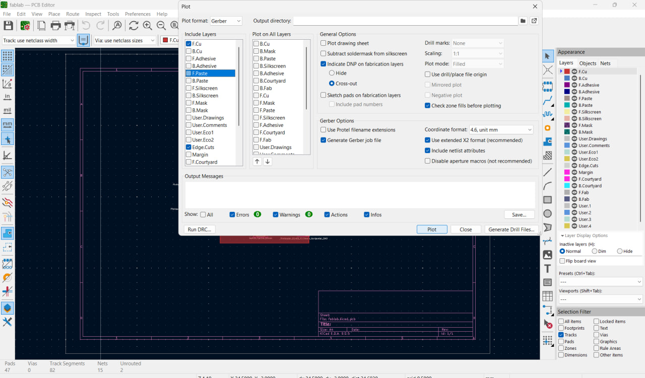
Gerber preview.
I used milling to make my pcb. The material of choice was RF4 boards.
Going to the machine I put my board in, used tape to hold it and tried to minimize the area that the tape was grabbing to have more area left over. Even tho the machine has a suction tape still helps with making sure the board still holds in place when there are more holes in it.
Then i checked the placement of the milling bit.
Next I selected an area for the boards
After that I calibrated the milling bit
Launched milling
During milling i need to make sure the bit doesnt keep the milling bit while changing since i dont want unnecessary damages to the lab equipment.
Then i went to soldering, honestly the solder and the iron were not good and the trace paths were too small so i ended up with a of solder on the board which I spred out and made look more artistic than a fail.