Electronics Production
This week’s goal was to characterize the design rules of our in-house PCB production process as a group, submit a PCB design to a board house, and individually make and test an embedded microcontroller system.
Link to our group page.
Introduction
This week focused on the transition from circuit design to in-house PCB fabrication, where design decisions had to be evaluated under real manufacturing constraints.
Up to this point, the process was mainly digital. With the introduction of in-house PCB milling, parameters such as trace width, clearance, pad geometry, and tool diameter became directly relevant for whether a design is actually producible.
One of the main learnings was that PCB design and fabrication cannot be treated as separate steps.
Instead, they form a tightly coupled system, where the capabilities of the milling process and even the soldering must already be considered during the layout phase.
For example, minimum trace spacing is not only a design preference but defined by the physical limits of the milling tool and machine precision.
The workflow therefore extends beyond schematic and layout design and includes the full chain:
schematic → PCB layout → CAM preparation → milling → soldering → testing
Each step introduces its own constraints and potential sources of error, which often only become visible in later stages.
Compared to industrial PCB production, in-house milling requires a more careful alignment between design rules and machine capabilities.
Tool wear, alignment, and calibration have a direct influence on the final result, making it necessary to validate and adapt designs accordingly.
The goal for this week was to better understand this relationship and to establish a workflow that produces reliable and reproducible results, rather than only focusing on functional circuit design.
Devboard PCB Design
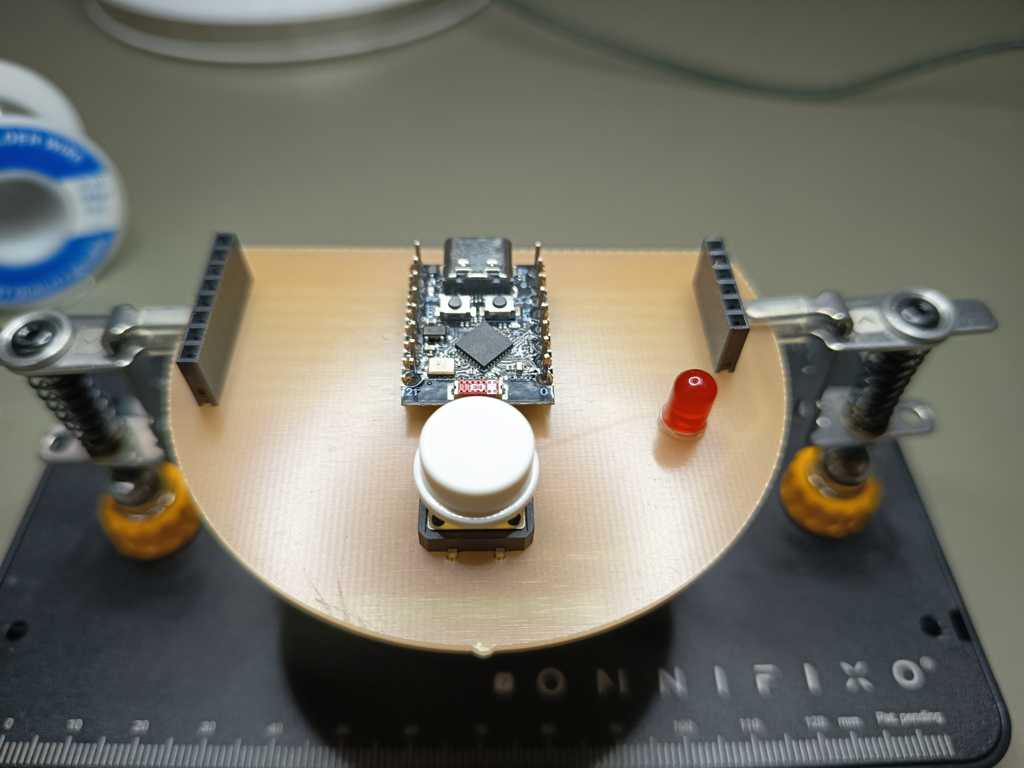
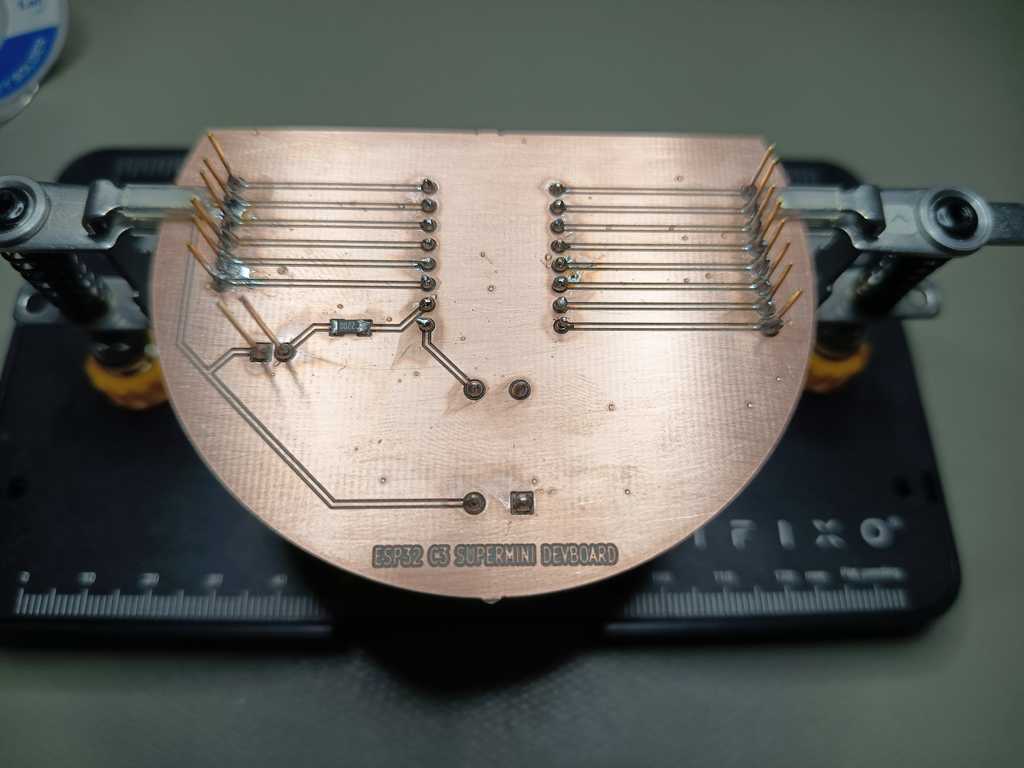
For this assignment, I designed a simple development board for the ESP32-C3 supermini to create a flexible platform for testing and further development of my final project.
The goal was to build a minimal but functional board that allows quick interaction with the microcontroller.
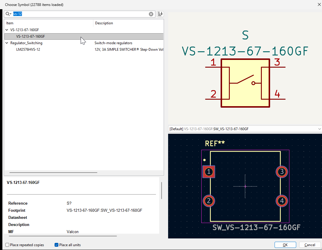
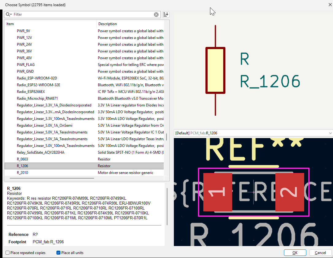
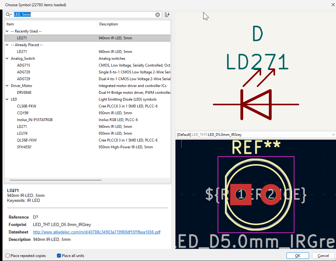
Therefore, I integrated a single LED with a 220 Ω resistor as a basic output and a [push button](https://www.snapeda.com/parts/VS-1213-67-160GF/Valcon/view-part/ as a digital input.
These components allow me to test simple functionalities such as blinking patterns or user interaction.
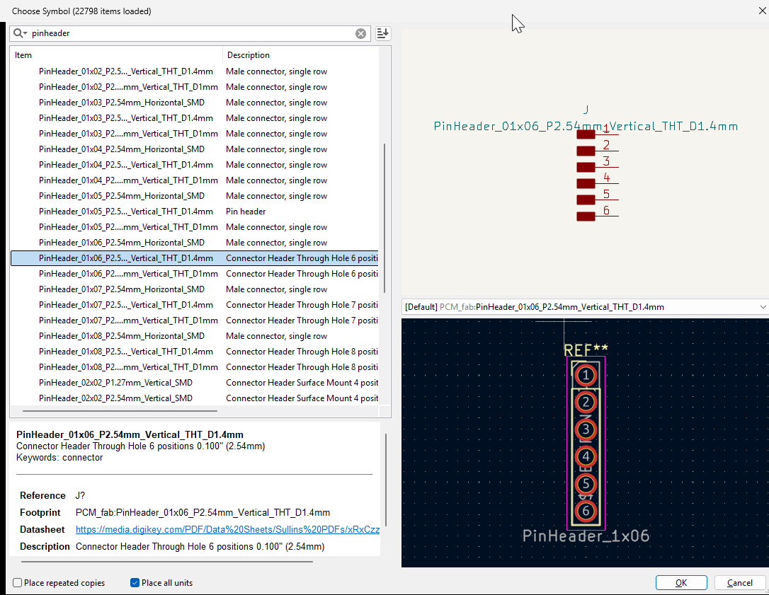
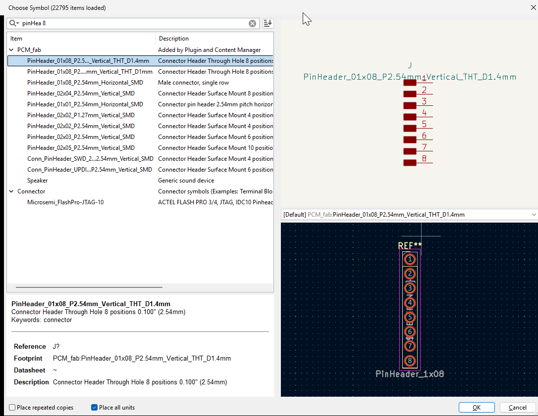
I connected all remaining GPIO pins of the ESP32-C3 to pin headers, so I can easily access them for future extensions.
This makes it possible to connect additional sensors, communication modules, or other peripherals without redesigning the board.
The focus of this design was not complexity, but usability and flexibility. The board serves as a development platform that I can reuse and adapt throughout the project.
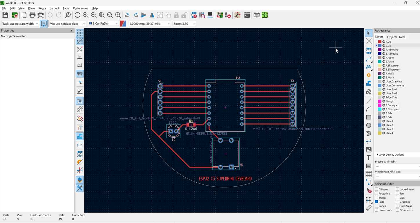
I started a new Kicad project, as in the previous weeks and added the components.
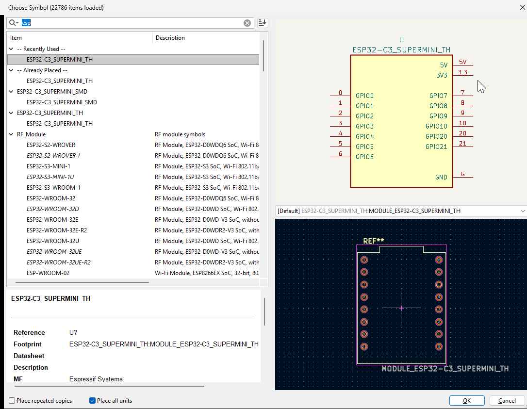
Then I connected all components in the schematic editor. After that, I updated the PCB editor and placed the components on the correct side of the board.

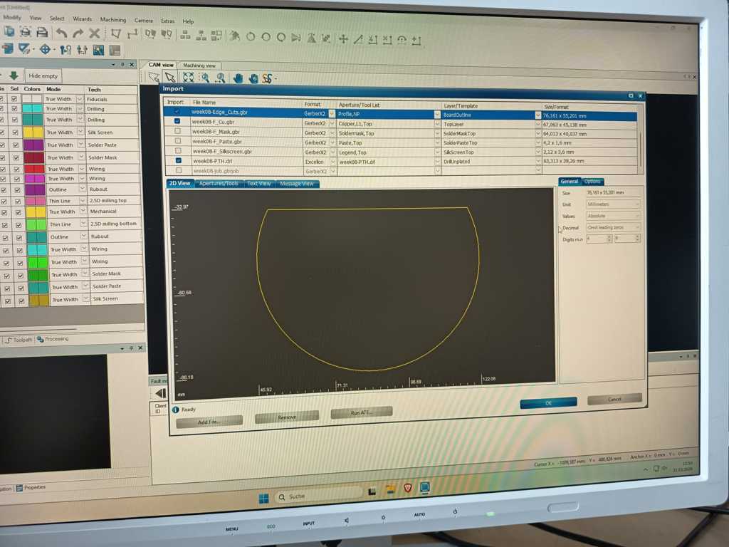
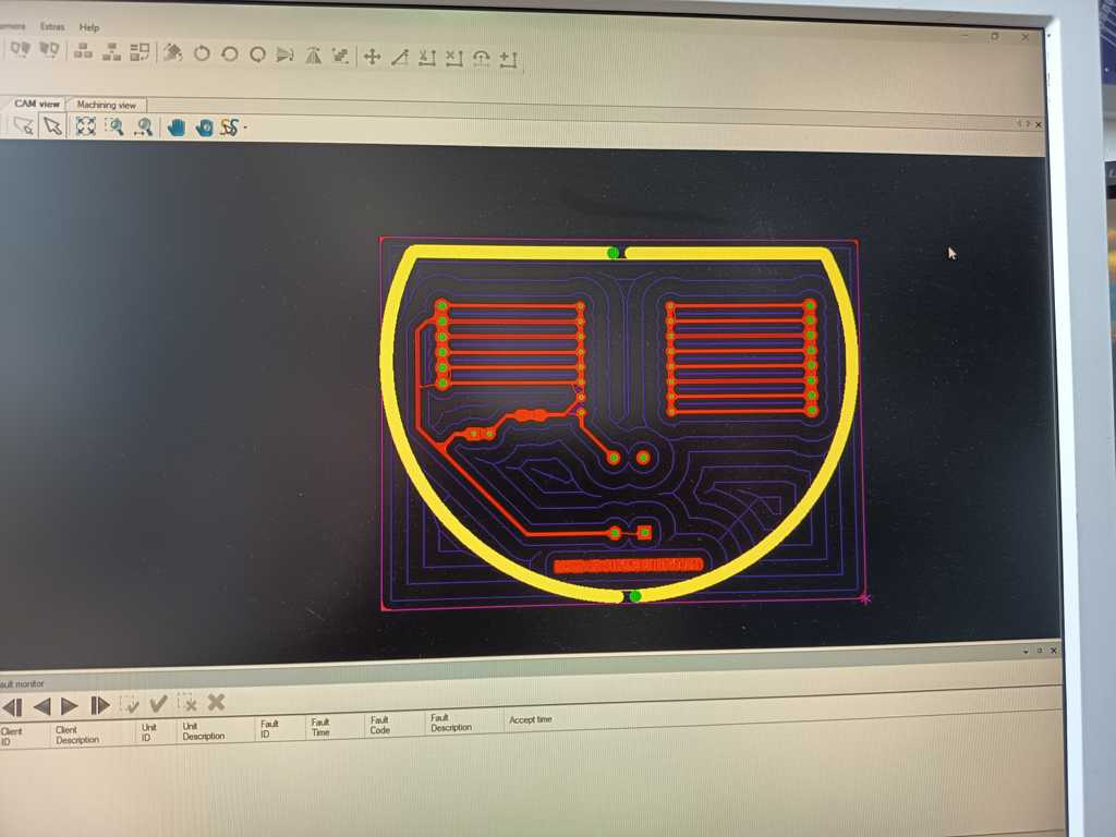
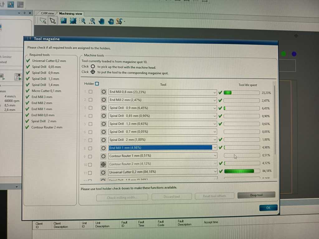
PCB milling
The PCB milling process is documented in detail on our group page. I followed the same workflow and started the milling job.
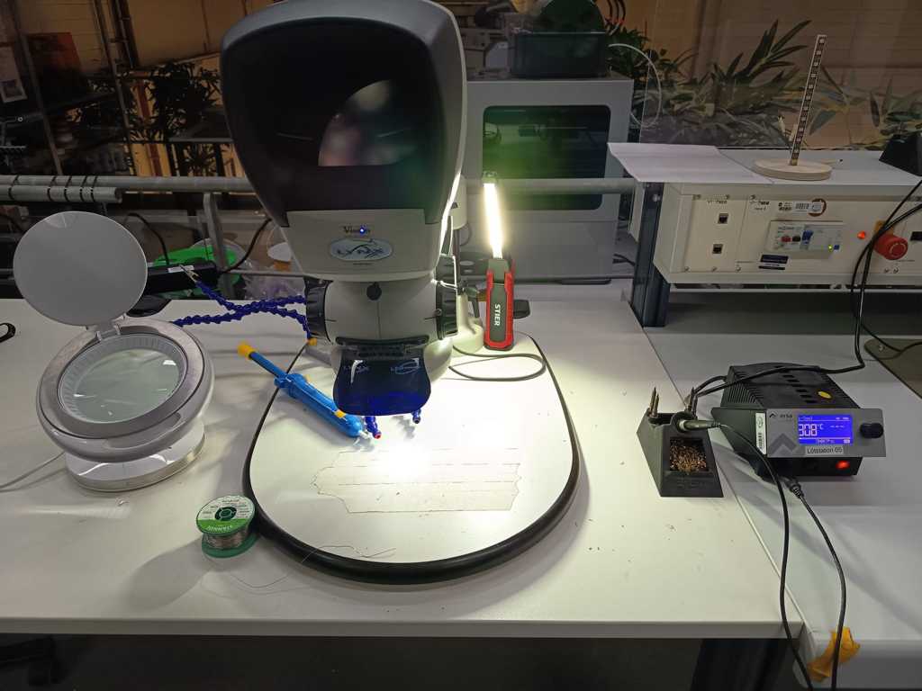
Then, I lightly sanded and cleaned the board. After that, I checked for shorts with a multimeter.
This was my soldering setup, and I assembled all components on the board.
Testing the Dev Board
Before I used the dev board in a larger circuit, I wanted to make a very simple GPIO test.
For this test I reused the small lamp from week 4, because it already had a WS2812B LED setup and was easy to connect to different pins.
I added a 470 Ohm resistor into the data line of the LED. This protects the data signal a little and is a common practice when working with WS2812B LEDs, especially during testing.
For the first check I uploaded a very simple blink sketch. While the sketch was running, I used the button input to trigger a short feedback sequence.
When the button was pressed, the status LED blinked three times. This helped me confirm that the button input and the basic board setup were working correctly.
In addition the sketch switches one single LED between full red, full green and full blue. I tested this signal on every remaining GPIO pin, one after another.
This helped me check which pins could be used as a digital output for the LED data signal.
Here is a short video of the test:
Downloads
week8_gerber.zip week8_code.ino