8. Electronics Design
This week, I designed, made, and tested out my own Dev board. Here’s the flow:
- Exploring Eagle on Fusion 360
- Experimenting and having fun
- Designing a basic LED-button circuit
- Designing my own Development board
- Milling
- Soldering
- Testing
Trying Eagle for EDA
Eagle is a part of Fusion 360 and I chose Eagle because I already use Fusion so I figured that it would be better if my PCB designing space is linked to my CAD space for better integration into CAD assemblies.
I looked at a bunch of tutorials in order to learn Eagle and would recommend you to do the same:
-
And of course, Jesal sir and his documentation.
Spiral 1: Exploring Eagle
As shown in the Tutorials, you will need to activate certain libraries to get the required components. You simply click on the Library Manager on the Left side panel and add the “Tutorials Fusion 360 library”. I also added the “Seeed Studio Xiao library” for getting the footprint of the Xiao RP2040.
Following the tutorial in #1, I made the following schematic:

Routing using various methods- straight perpencdicular lines, curves, diagonals. Rest done via autorouting.

Using the Polygon tool.

Final board outcome (even changed the board shape) for the exploration. It’s, by no means, a functional PCB- just meant for me to explore various software tools.

Spiral 2: Basic LED-button PCB
Next I took the program I had done during the embedded program week and converted it into a schematic on paper.
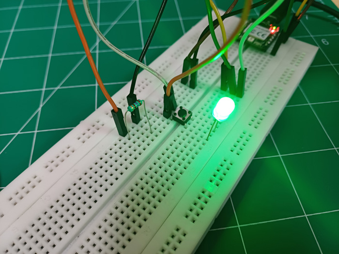
The basic concept was that you press the button and the LED will glow.


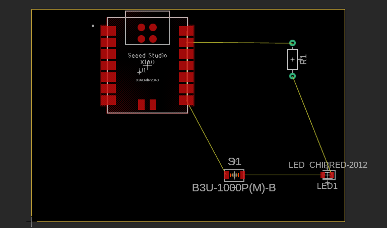

Here I realized that the track width was too low. So I increased it.
I also added my name ‘SID’ to it using the Polygon tool. I also gave random curvy lines for fun!

The track connecting the Pin and VCC was going underneath the RP2040 and had a high chance of merging with the pads. So I reworked the routing.
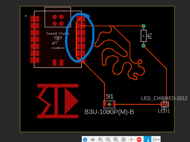
I also added my name’s shortform SID as an emblem mark on the board. First I used the Polygon Cutout tool, then I used the Polygon Pour from Outline tool to create path outlines.

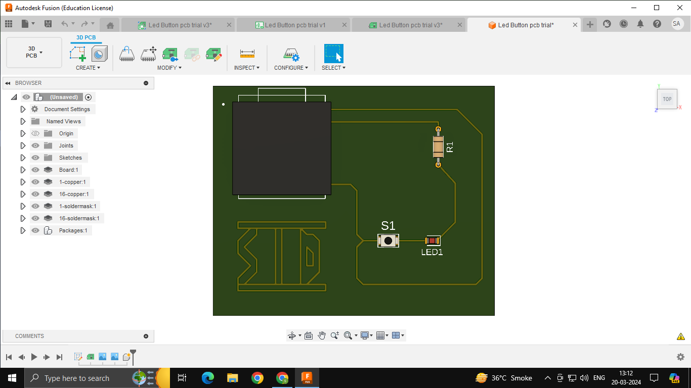
The final outcome of this:


Spiral 3: Making my own dev board!
Next, I made the schematic based on Jesal sirs work and guidance. I took the SV, GND, and 3V3 connection and connected each of them to 6 header pins. I even gave extra pins for I2C and SPI pins. The purpose of this Dev board was to be a breakout board, in the sense that it should integrate with the Xiao RP2040 in such a way that all the pins of the Xiao are exposed properly and there are extra pins for frequently used areas like 5V, GND, 3V3, I2C and SPI.
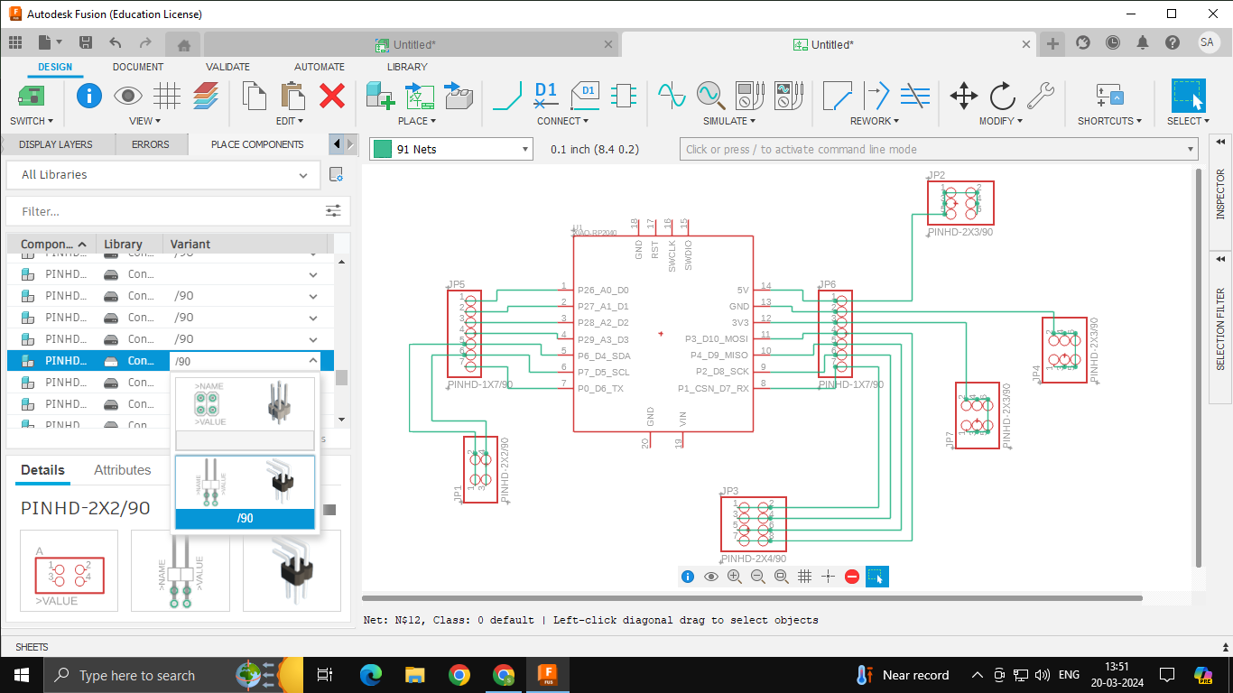
I started out with the basic schematic. Here, it is simple as you just need to drag and drop your component and it automatically shows you the footprint/schematic.

Then I went on to align the components using the Align tool.
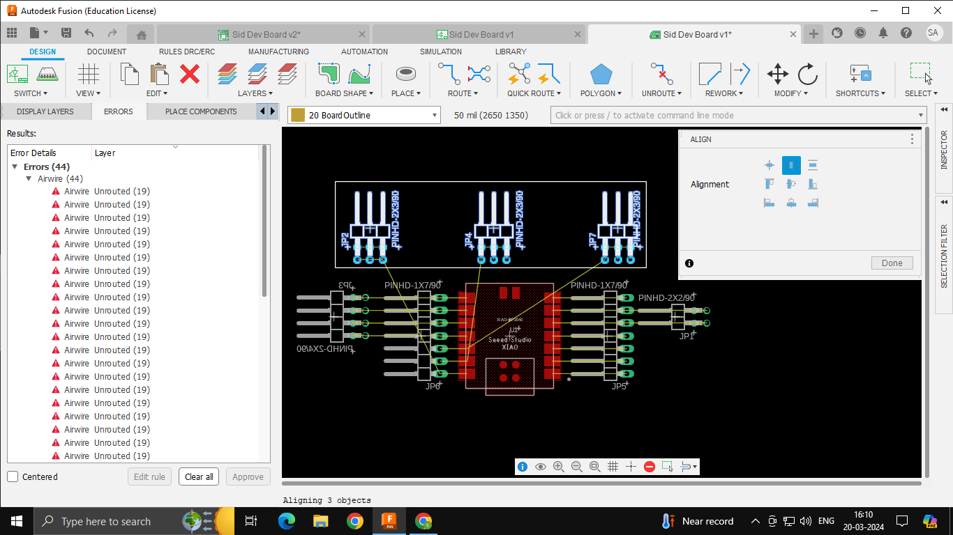
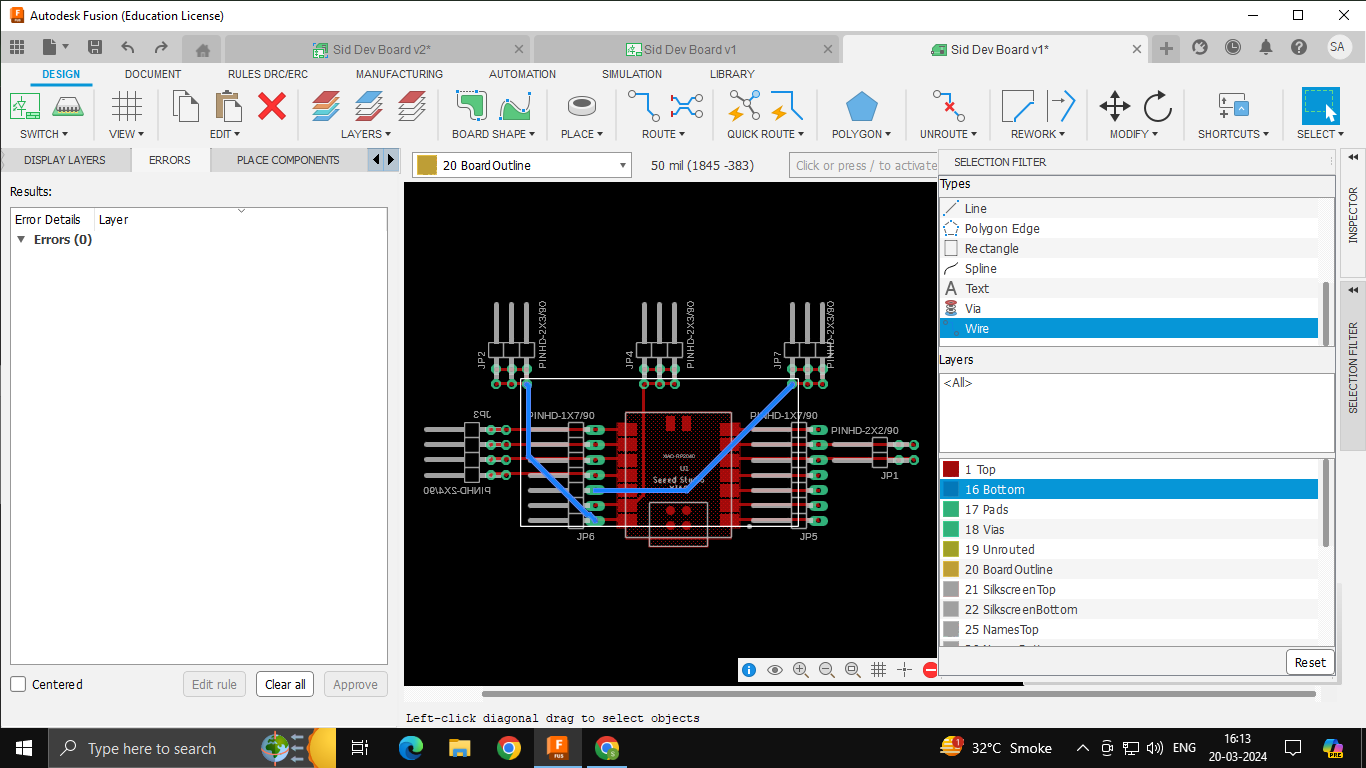
Here you can see that this became a ratsnest, meaning that are connections on the schematic but not on the PCB. The “airwires” show the shortest route between two components. However, these are straight lines and overlaps with each other and the components. A rats nest typically needs to be routed.
I decided to start by Auto-routing it.
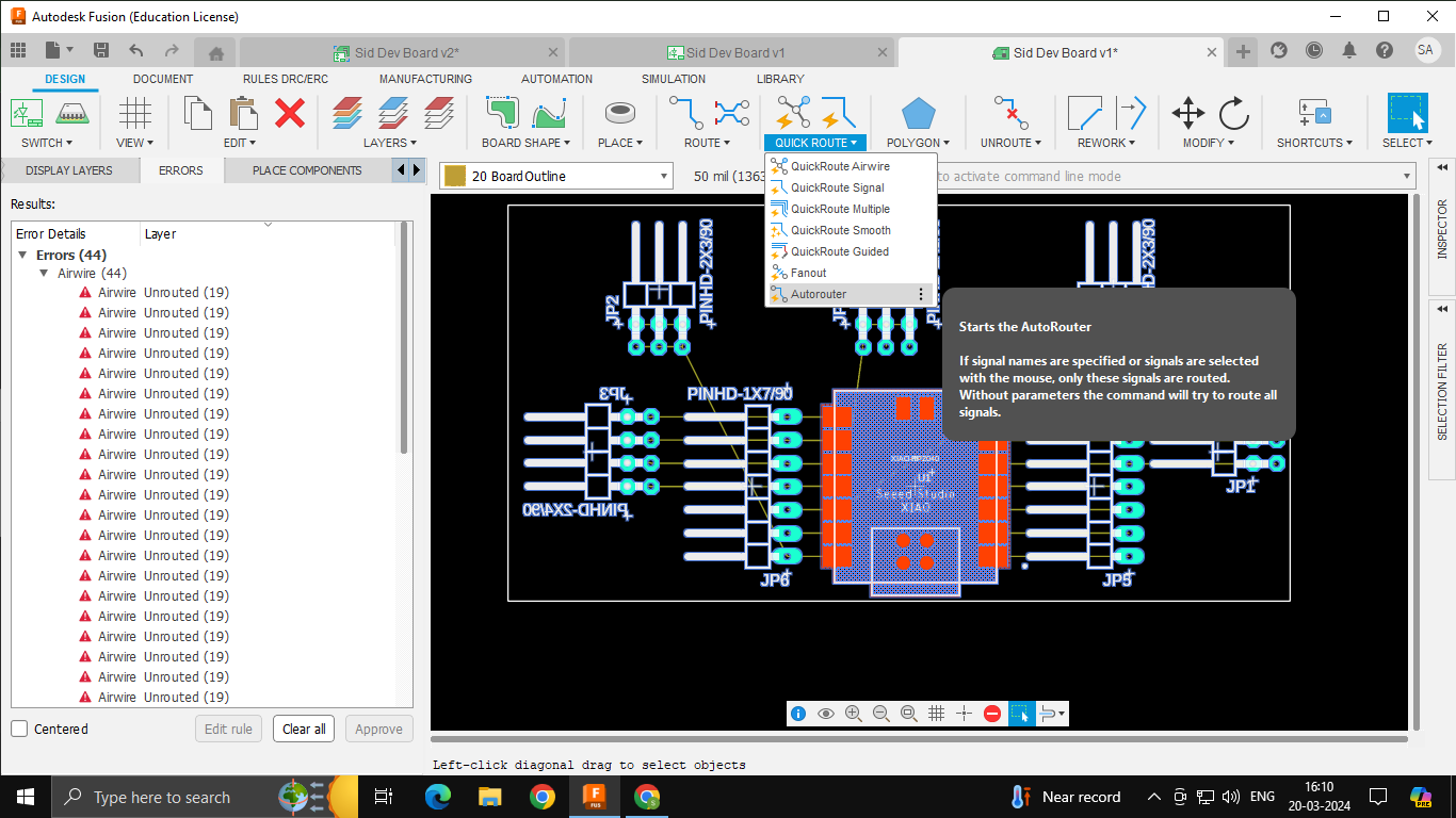
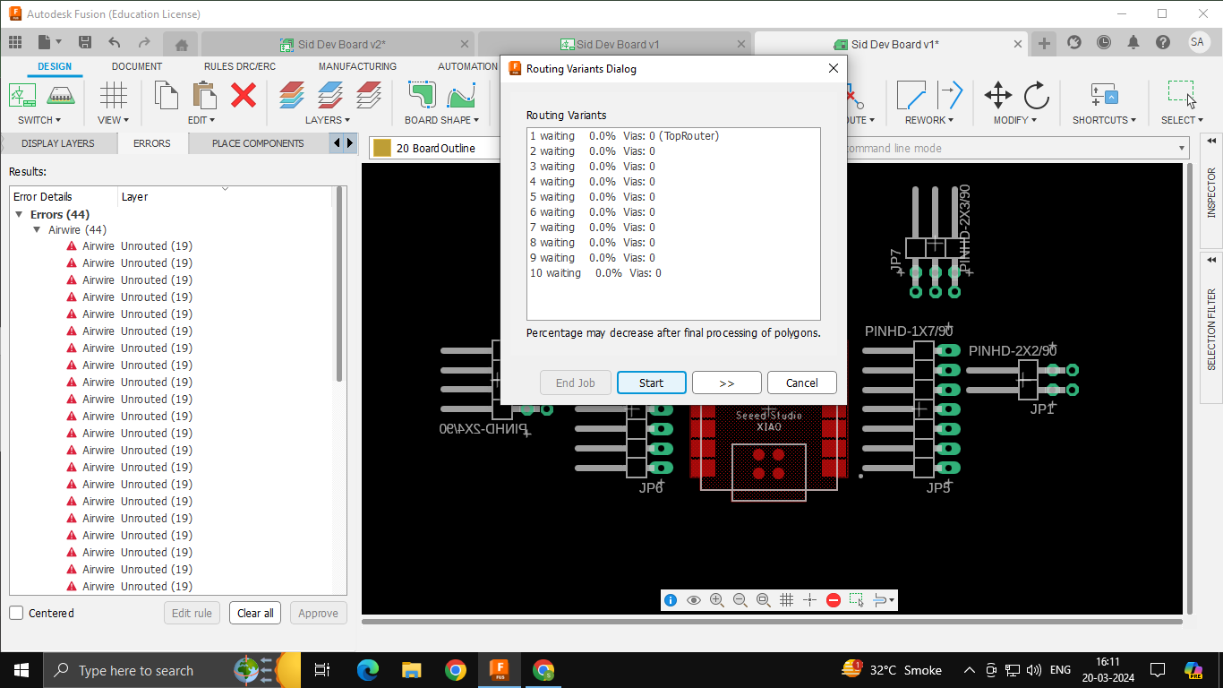

As you can see above, the auto-routing caused a few tracks to be on a different layer. Since I was going to mill them all on one layer, I needed to shift the blue tracks to the red layer.

I used the Selection Filter on the Right side to select just the Blue tracks and then moved it.
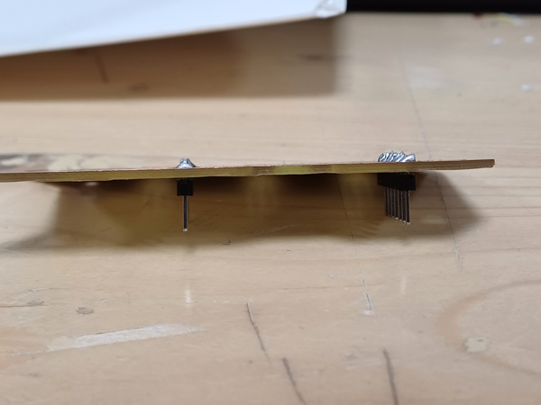
I got to this point, arranged everything and realized that my pins were wrong! I was planning to use the straight header pins, not the 90 degree bent ones. So I had to go back to replace them.
The replace feature on Eagle was really good. You just had to select which pin you wanted to replace and to what.
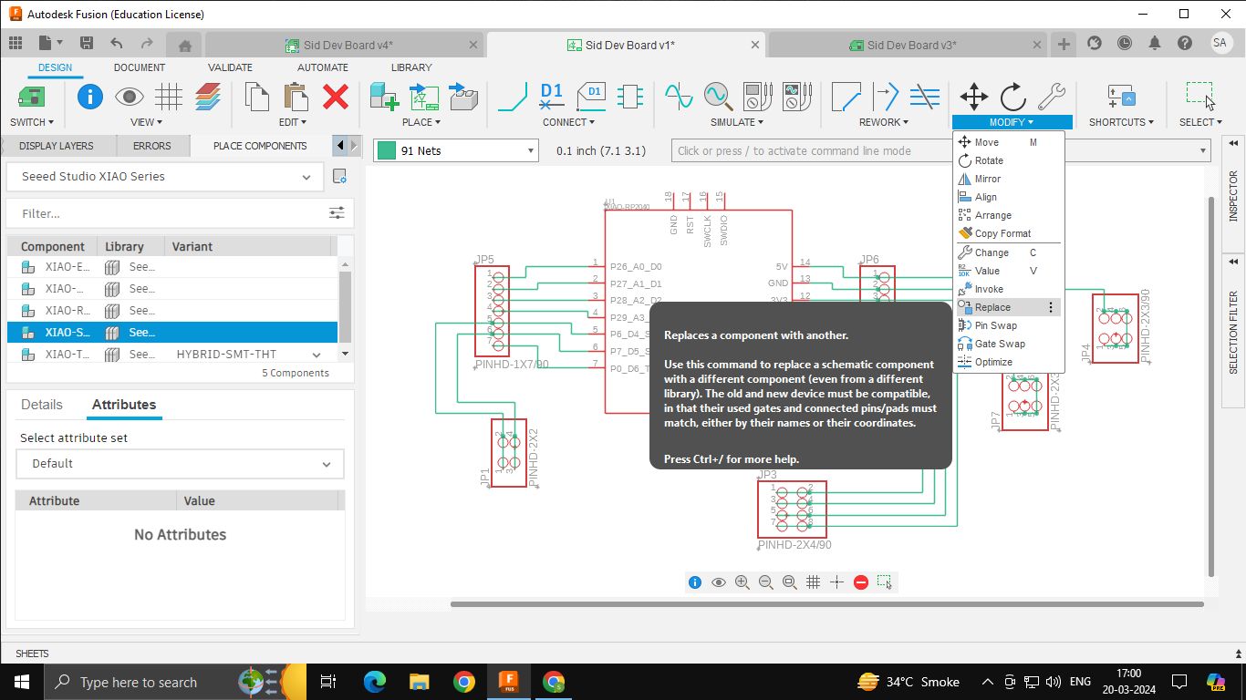

And it worked!
Before:

After:

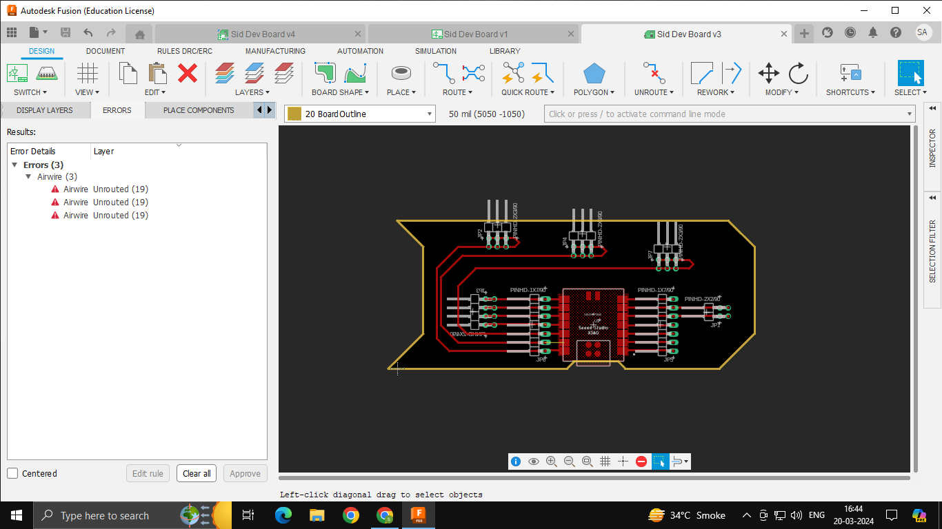
And finally I arranged them!
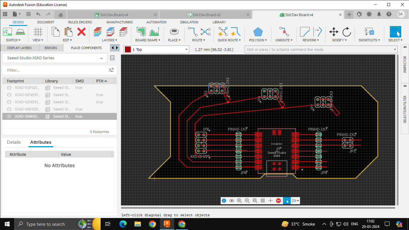
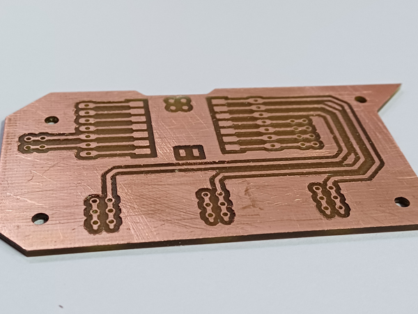
The final board design:

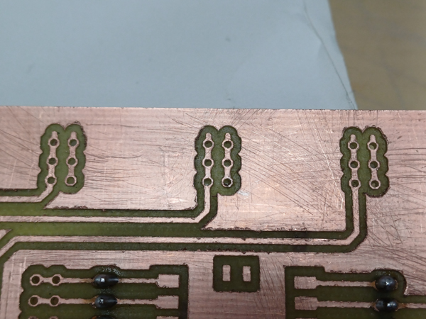
Since I had only header pins on my board (and no LEDs or resistors), I chose to keep the layout simple. I simply extended the route along a tangent from the Xiao board and set the pins there. For GND, 5V, 3V3, I chose to go around have the three lined up along the lower edge of the board. This way they would be evenly spaced and recognizable.
To further add to this, I gave the board direction. I chose a shape for the outline which signified motion, to relate to the “flow” of current. Moreover, this asymmetry of the board made it easier to recognize the pins once it was milled. It became easier to remember which pins were where.
I wasn’t very confident with my soldering and based on what I learnt in Week 4, I knew that I needed the tracks to be a certain width, and the pads to be a certain width [Track width = 0.7 mm, Pad width = 1.7 mm]. I also knew that I could change these widths on CopperCAM itself before milling.
I did the DRC after making the PCB. In the DRC, I changed all the “Clearance” values to 16 mils or 0.4064 mm and the Copper/Board outline to 40 mils or 1.016 mm. Drill hole value remained at 6 mils or 0.1524 mm. These values were recommended to me by Jesal Sir. He said it is what he used and would recommend because it is a safe disctance/clearance to have in case soldering goes bad. However, on applying and checking DRC, I got a series of errors because I had already routed the tracks. So, to change the track widths, I went to the Command line of Eagle and typed
CHANGE WIDTH 0.4064and pressed Enter. This made my cursor into the “+” icon and any track I selected after that turned 0.4064 mm wide. Either way, I ended up changing the track width to 0.7 mm and Pad widths to 1.7 mm on CopperCAM as mentioned earlier.
Milling
I started out by exporting the gerber files from Eagle.
To do this, go the manufacturing panel and then under Manufacturing, select Export as Gerber etc.

Then click OK, you will now have a zip file containing Gerber files, board outline, and drill files.
Then I began importing the gerber files to the CopperCAM software which we use for milling PCBs. I used the SRM-20 Machine to mill the PCB. You can learn more about the usage of the machine- the How tos, the right settings etc in my week 4 documentation
The engraving contours and the cutout went to the right layer and I could manually Right Click and use the “Center Horizontally” and “Center vertically” to get them aligned in place. However, the Drill holes were all over the place. Some were in the right spots while others were not. Reopening the file didn’t help either.
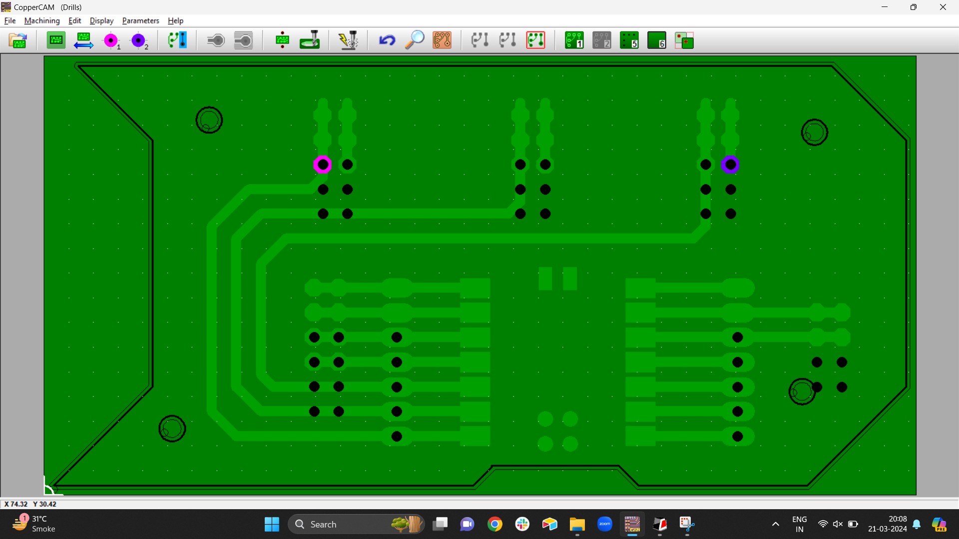
So, here’s how I tackled it: First, I set a drill pad as a Reference point and adjusted all of the holes so that maximum holes were on their respective pads. Then, I removed all drill holes which were not in position. This left me with a good number of spots which had the drill holes rightly placed and a few places which needed drill holes but didn’t have it.
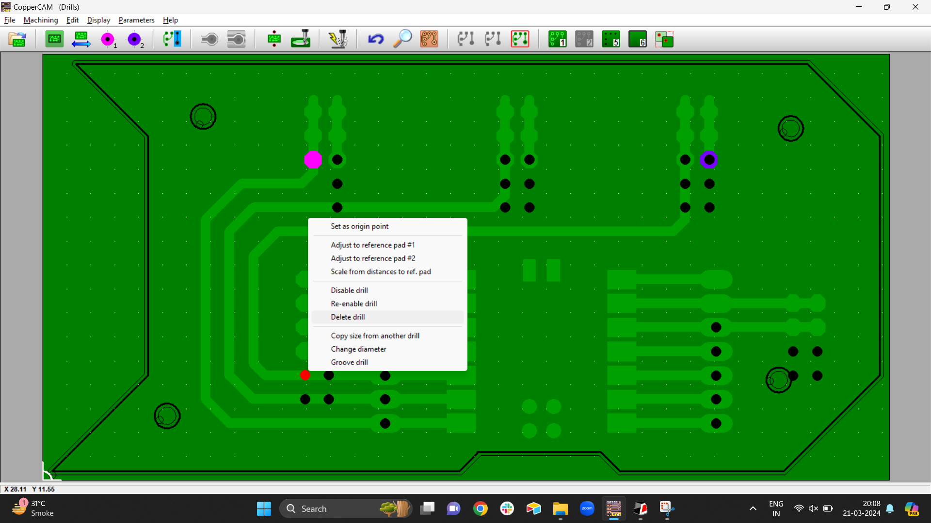
I went ahead and drilled the right ones out. Next, within the CopperCAM software itself, I set the empty spots as a Reference Point and moved all drill holes to the reference point. I deleted all drill holes which were out of place.
I made sure not to change the origin on Vpanel. This way, in subsequent drilling iterations, I was able to get the machine to drill all the holes.

Dev board being milled:
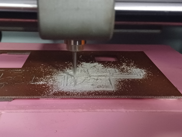
It turned out quite burred. I’m not sure why, maybe the plate was warped. To deburr, I took a piece of sand paper and lightly sanded off the board. It worked well!
Before:


After:

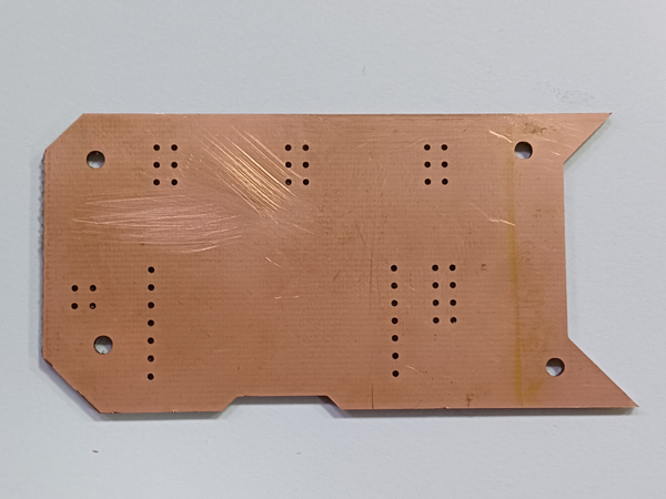
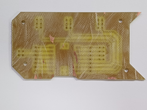
Then, something dangerous struck me- almost like lightning. I had used the wrong copper plate to make the dev board. See, the thing is, I wanted to make a through-hole soldered PCB, and NOT a Surface mount one (Primarily becuase soldering SMD was really tedious for me). However, I goofed up and used a double-sided copper plate. That meant that all my thorugh hole components and pins would DEFINITELY be shorted.

I didn’t have enough time to mill another one as our lab was closing for the day, and given the time our milling machine takes to mill a PCB, I would be stuck for another 20-30 minutes easily. Plus, I was leaving the city the next day so I had to get my dev board ready that night.
I used a Jugaad and decided to bulldozer it. I know it’s not the best approach to things. But it did work out well.
Here’s what I did: I used an Angle Grinder with the Sanding Blade and carefully sanded off the layer of copper at the back.
This is what my Dev board looked like post that:
Before sanding:
After sanding:
I know this isn’t the best option but done is better that perfect :/
Soldering
I started out by soldering the male header pins. In through-hole components, the soldered part rests on the top surface (the copper pad) and the actual component most likely rests on the underside of the board.
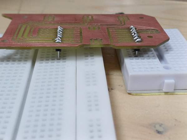
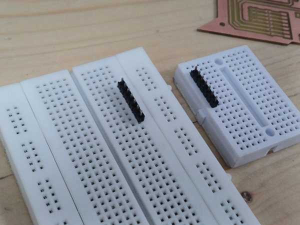
It is advisable to use a a bread board to hold the pins in place while you solder the top.

I realized that the machine had missed a semi-circular path which connected these lines of pins:
I decided I would just solder them together. However, I ran out of time and chose to solder only a basic amount of pins which I would require, and not the extra ones.
Hero shots


Testing
Finally, I used a multimeter to check if the connections were correctly made or not.
I set the multimeter to do the Connectivity Test so that it beeped and showed a value when the two probes were connecting. I kept one probe on the soldered Pad/hole which was at the beginning of the track, and the other probe at the other end of the same track. With this, I was able to ensure that all connections were good and there was no shorting due to excess solder or any other reason.
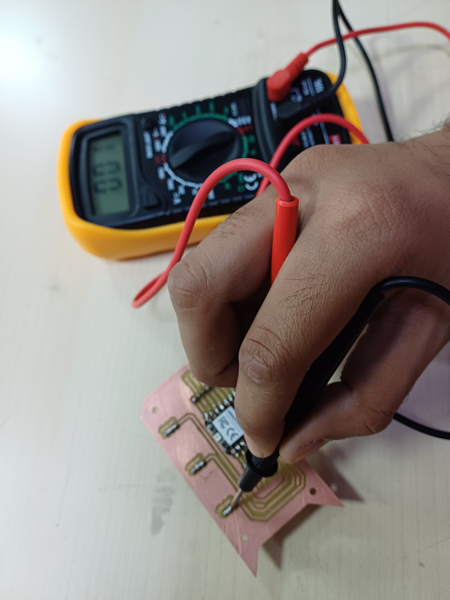
In this image, I am connecting one probe to where the soldered pins are. The other probe would connect to the other end of the same track which is soldered at pin of the XIAO. However, I was not able to take an image of the multimeter test correctly as I was the only one there and needed to hold the camera in one hand.
Thankfully, all the connections were connected well.
Next, I tested out my Dev board.
I started out by blinking the RGB on the Xiao RP2040 board. And then I went to connect an LED and a button and put up the basic code to test that out.
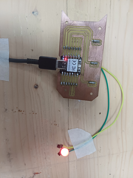
I used the Example Blink Code. You can find more about programming the Xiao RP2040 on my Week 6 Documentation.
Send out a PCB to a board house [Group work]
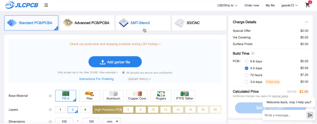
We availed services of the board house JLCPCB to place an order of the QT v1 board. We did this with the help of Pranav sir.
The landing page greeted us with various features of the board house. We logged in and clicked on “Order now”.

Here, we chose from the 4 different types of outcomes we desired and went ahead with the standard PCB.
We added The gerber zip files to Adrian’s QT v1. Once that happened, we could see the board layout in a small box on the page.
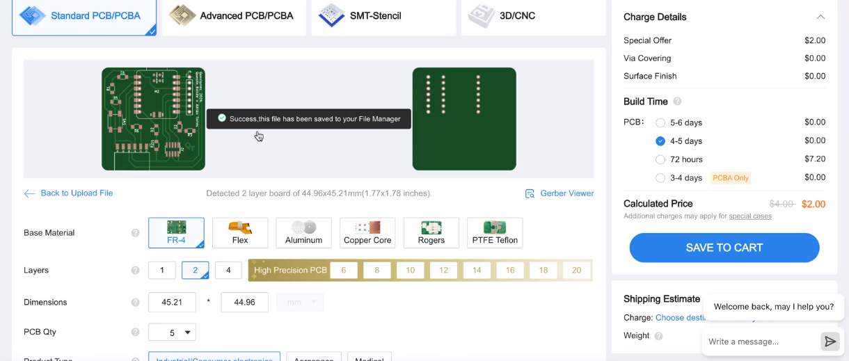
Something to note here is the unique User Interface, which allows the user to know about every technical term mentioned. For the base material, simply hovering over showed you how the base material looked and what its features were.
We chose the FR4 base and set the order quanitity to its minimum, i.e, 5.

We went ahead and chose black as the color along with a white silk screen. Immediately, the diagram above reflected our color choices.
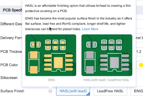
We stuck to the default surface finish of HASL(with lead).
Another UI point to mention here is the tiny ‘?’ symbols near the criteria name. This helps you understand the criteria and its contents better.
The ‘?’ about Vias:

We finally gave in the final bits of detail:
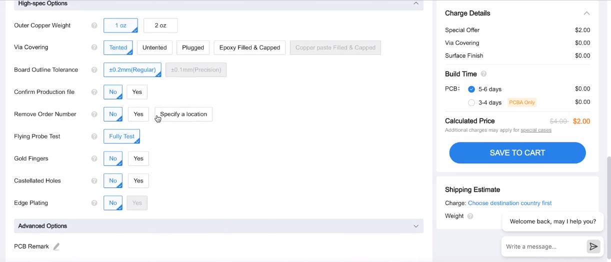

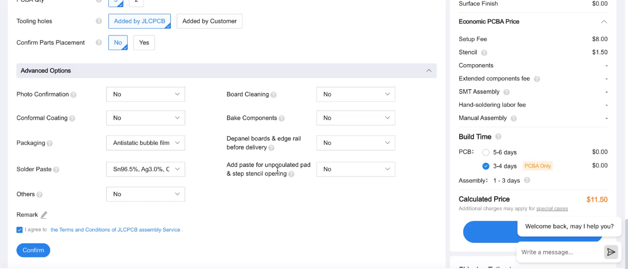
Proceeded to checkout. The PCB is in the cart!
Here, we learnt that JLCPCB has a unique feature where you can lock components into your cart without paying for it immediately. This allows you to block items for you before they run out of stock, and you can pay and have them delivered at your own convenience!

And finally, feeding in the address of delivery:

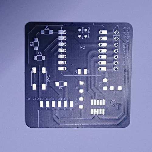
PCB on arrival:

Oscilloscope [Group work]
Please find this week’s group assignment iteration 1 on Himanshi’s Page. Search for Group Work heading. We used the B&K Precision 2194 Oscilloscope. You can find the manual, datasheet, and more information about it on their official website: https://www.bkprecision.com/products/oscilloscopes/2194
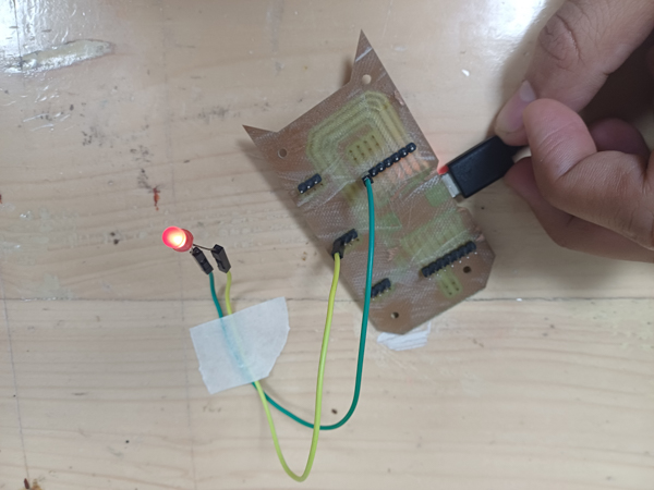
In the second Iteration, we used the MINIWARE Pocket Oscilloscope DS211 for plotting the voltage signals over time. We used the PCB made by Tejas in Week 8. He had an LED soldered on to his PCB which connected to the Xiao RP2040 pin D7. We ran the Fading Example code on the arduino IDE and connected the positive probe to the LED and the negative aligator clips to the GND pin.
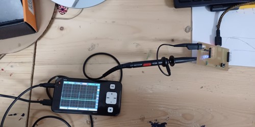
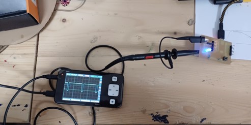
In the video below, you can see the fluctuating waves on the oscilloscope due to the PWM. The voltage is plotted on the Y-axis and time is plotted on the X-axis.
Project Files:
Sid’s Dev Board Zip file GERBER
Sid’s Dev Board Eagle file f3z