Electronics Design
Another challenging and difficult week
Delving into the intricacies of electronics, Neil's comprehensive session served as a much-needed refresher on foundational concepts such as Ohm's Law (V=IR), along with detailed explanations on the roles of capacitors, resistors, and inductors. Furthermore, the exploration of advanced components like MOSFETs and transistors offered insights into their applications and functionality, enhancing understanding and proficiency in electronics design.
This week's assignment was to Use an EDA tool to design a development board to interact and communicate with an embedded microcontroller and group assignment was to Use the test equipment of our lab to observe the operation of a microcontroller circuit board (as a minimum, and demonstrate the use of a multimeter and oscilloscope)
All the basics of electronics I did in week 4- electronic production because electronics is something which was totally new for me and I did not wanted to jump directly on the milling as I was not understanding anything so I did it before, you can check the documentation in this link
Designing a development board with an embedded microcontroller
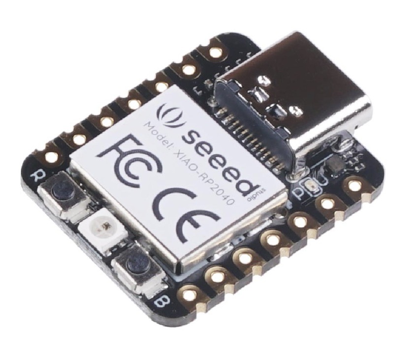
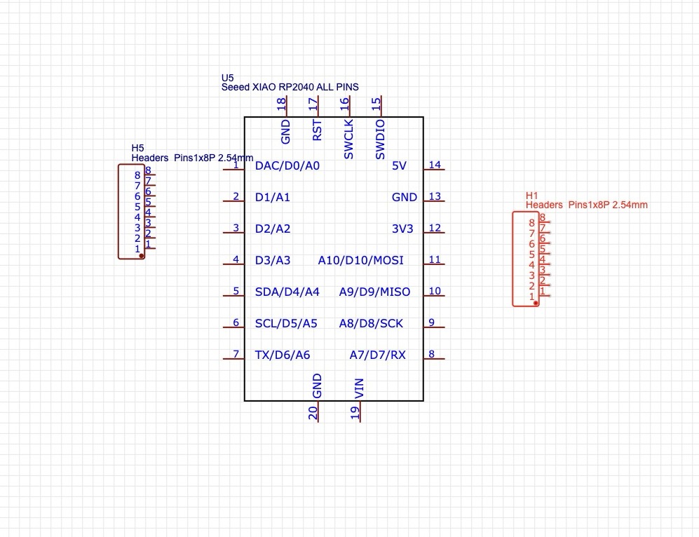
Foe this week's assignment I am going to use RP2040 Micro controller.
RP2040 is a microcontroller chip by Raspberry Pi Foundation. It features a dual-core ARM Cortex-M0+ processor, offering versatility and cost-effectiveness. With GPIO pins, UART, SPI, I2C, PWM, ADC, and more, it's suitable for various applications like embedded systems, IoT, and robotics. Its affordability and ease of use make it popular among hobbyists, educators, and professionals. Everything related to RP2040 can be found Here
Block Diagram of RP2040
Understanding RP2040
For this week's assignment I used RP2040 as the embedded microcontroller to design our development board to communicate and interact with. At first, it was a bit scary as I had no idea what to do next!. So I started with understanding the micro controller.
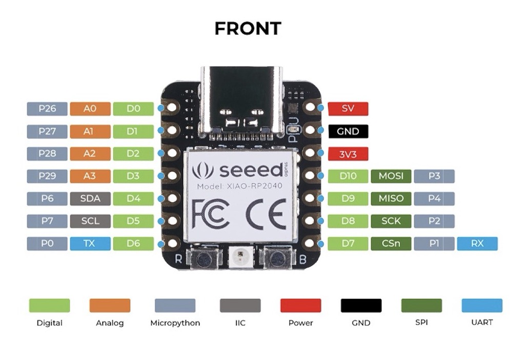
Starting with understanding the pins on RP2040
VCC (3.3V):
This pin provides regulated power at 3.3 volts. It's used to power external components or sensors connected to the board.
GND (Ground):
Ground pin, used as a reference voltage for all circuits on the board. It completes the electrical circuit and provides a return path for current.
Digital I/O Pins:
RP2040 offers multiple general-purpose digital input/output (I/O) pins. These can be configured as either inputs or outputs in your program and are commonly used to interface with sensors, actuators, and other external devices.
Analog Pins:
Some pins on the RP2040 support analog-to-digital conversion (ADC). These pins can read analog voltage levels and are often used to interface with analog sensors like temperature sensors, light sensors, etc.
PWM (Pulse Width Modulation) Pins:
Pulse-width modulation pins allow you to simulate analog output using digital signals. This is useful for controlling the brightness of LEDs, the speed of motors, and other applications where varying voltage levels are required.
UART (Universal Asynchronous Receiver/Transmitter) Pins:
UART pins allow serial communication between the RP2040 and other devices like computers, other microcontrollers, or peripherals. They include transmit (TX) and receive (RX) pins.
I2C (Inter-Integrated Circuit) Pins:
I2C is a serial communication protocol commonly used to connect multiple devices in a master-slave configuration. It uses two pins: SDA (data line) and SCL (clock line).
SPI (Serial Peripheral Interface) Pins:
SPI is another serial communication protocol used for high-speed communication between microcontrollers and peripheral devices like sensors, displays, and memory chips. It typically uses four pins: MOSI (Master Out Slave In), MISO (Master In Slave Out), SCK (Serial Clock), and SS (Slave Select).
RESET Pin:
This pin is used to reset the microcontroller. Pulling this pin low will reset the RP2040, restarting the program execution.
Boot Mode Selection Pins:
These pins are used to select the boot mode of the RP
Exploring the software
PCB design can be done on multiple softwares such as EasyEDA, Autodesk Eagle, KiCAD, etc. I started with easy EDA and continued with that as it's UI was easy to understand and I found the software to be easy to use.Another benefit of the EasyEda software is that you can directly order the PCBs for printing/mass printing from the JLCPCB.
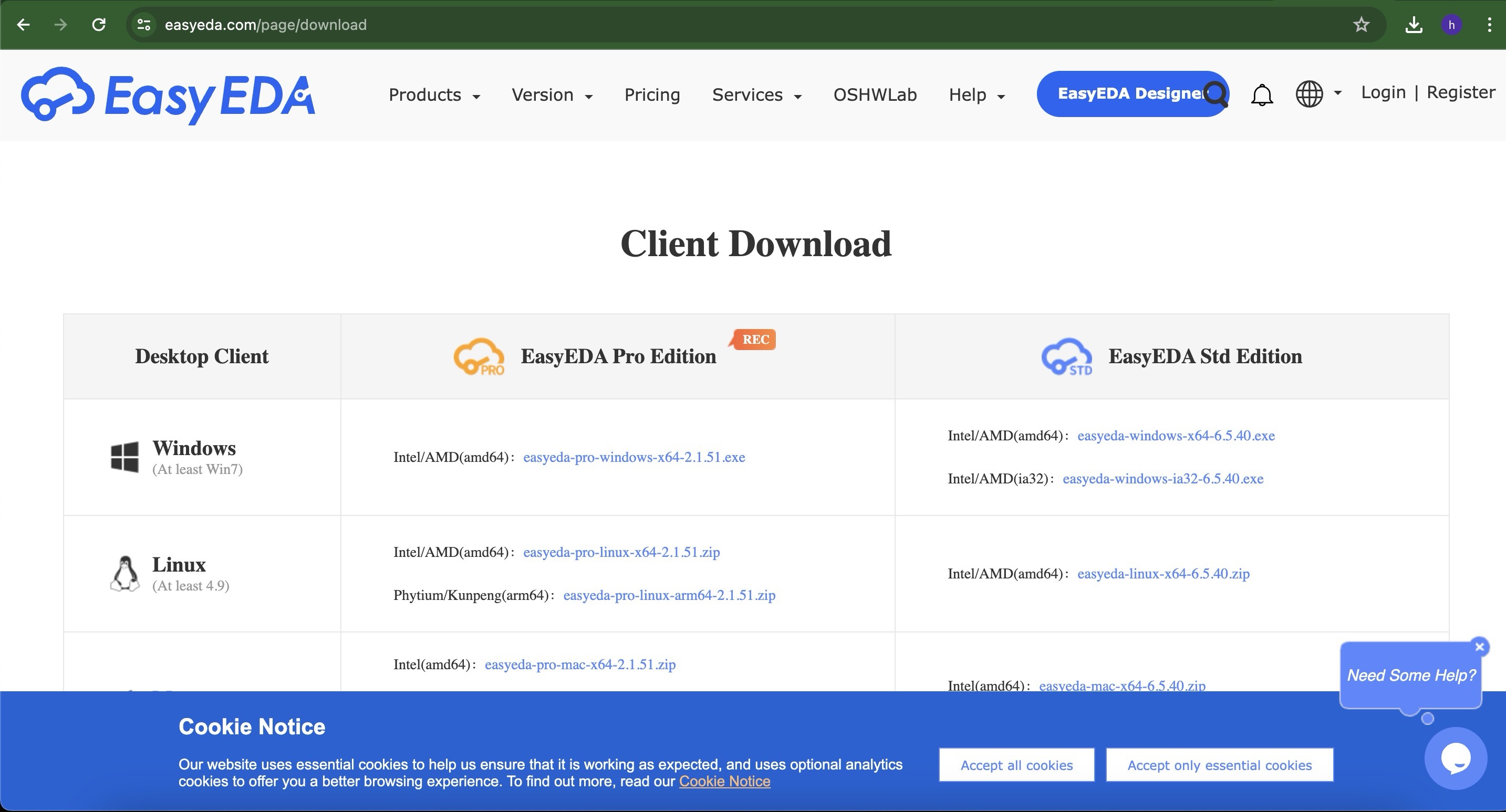
Download the Easy eda software from the official easy eda website, link of the website
The basic interface of the app looks like this:
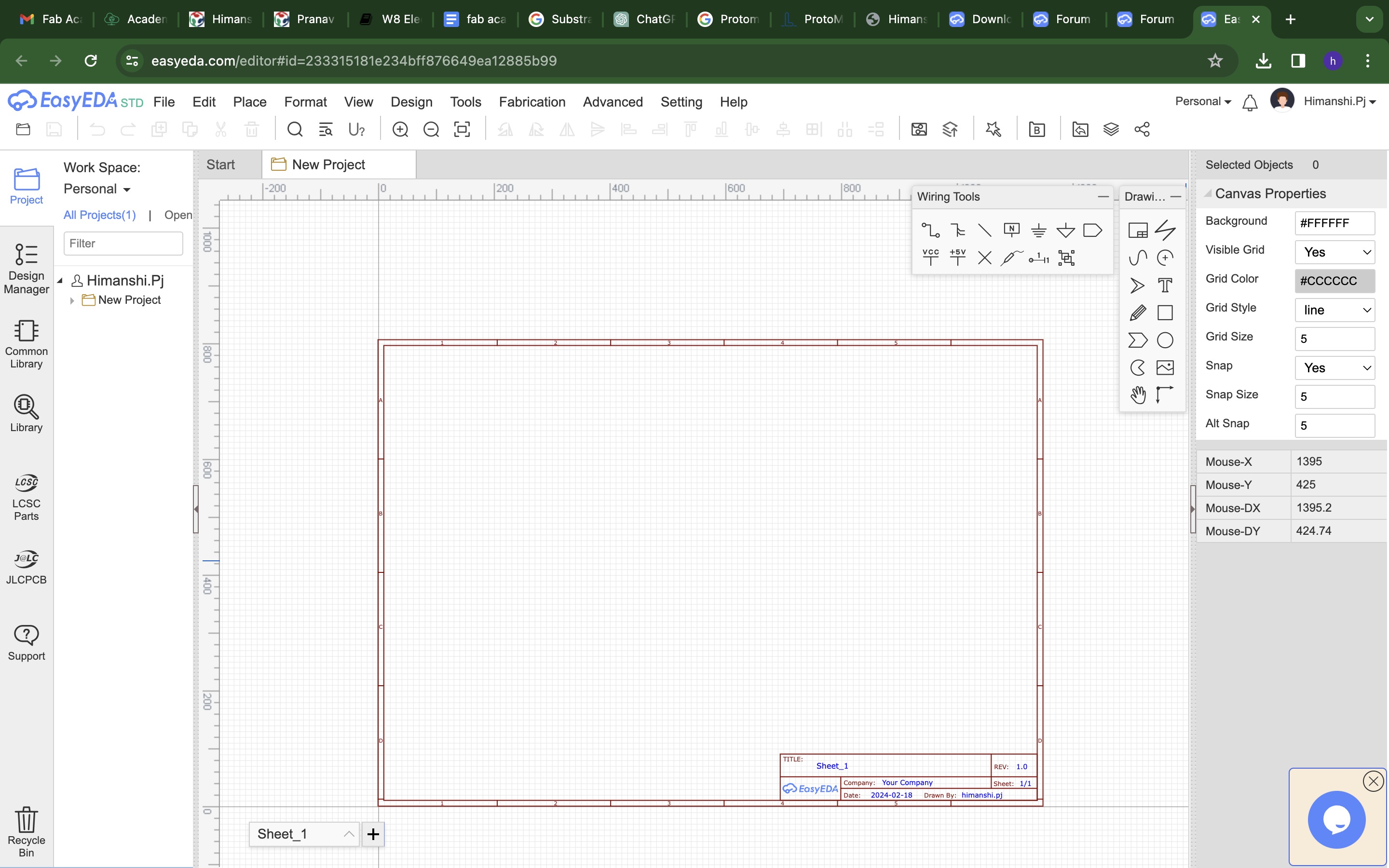
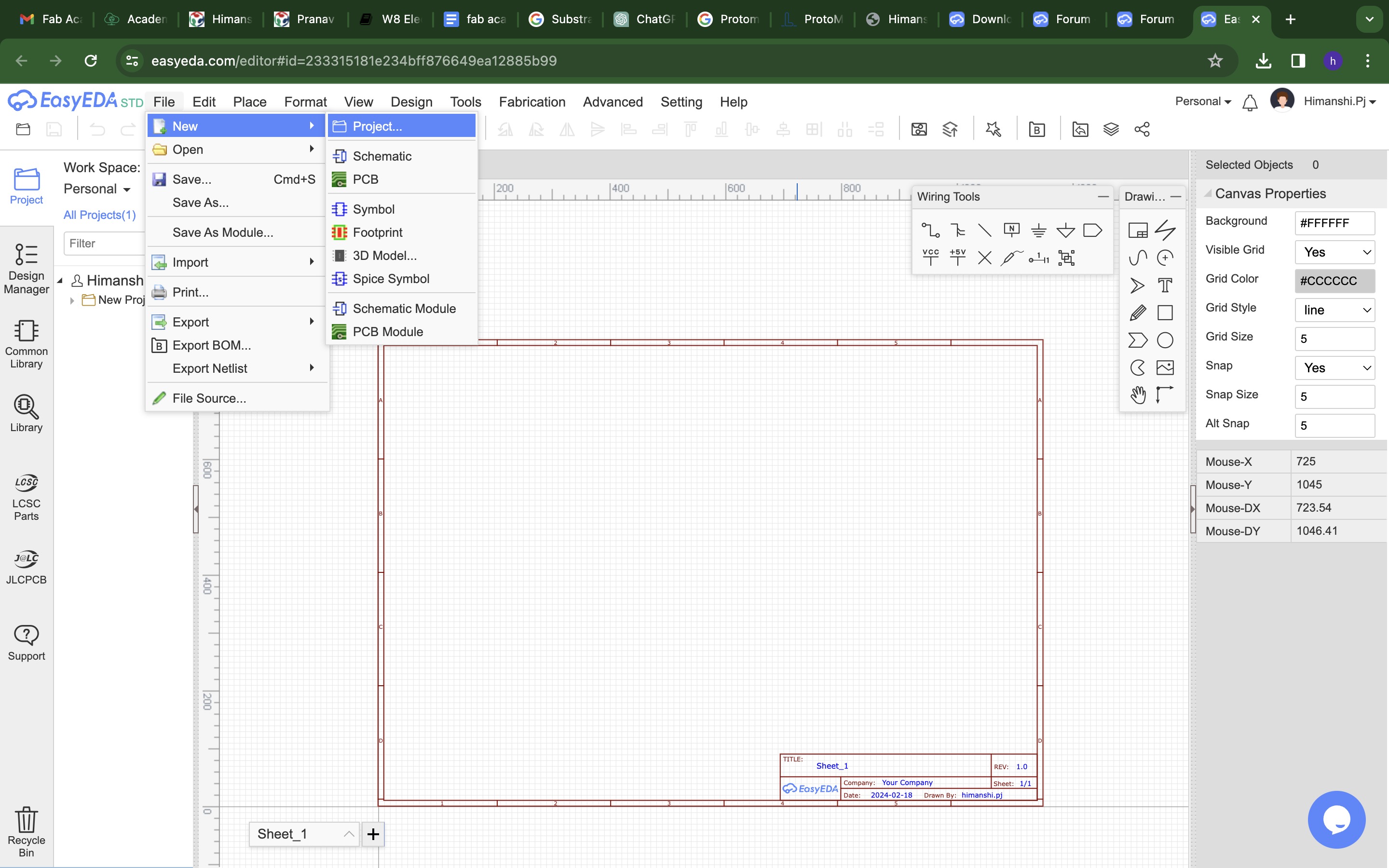
To start designing, FIle > New > Project. Then initiate a new schematic to start first.
To start importing electronic components, open the library panel and enter the name in the search window as shown in the figure below:
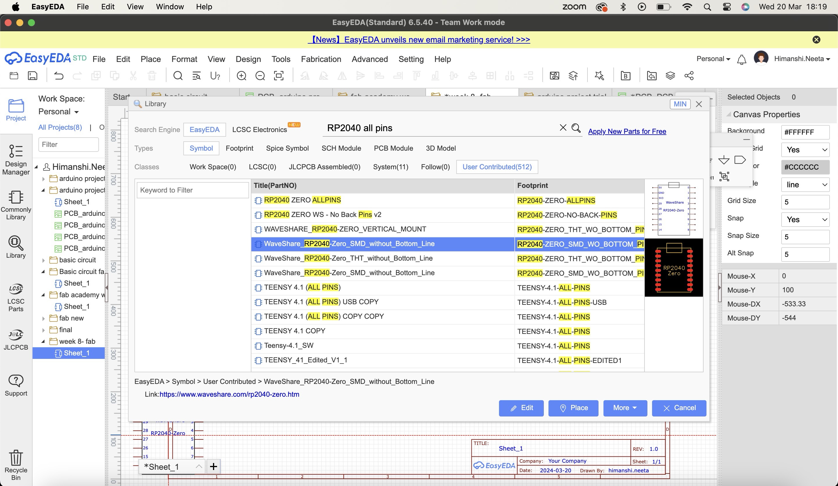
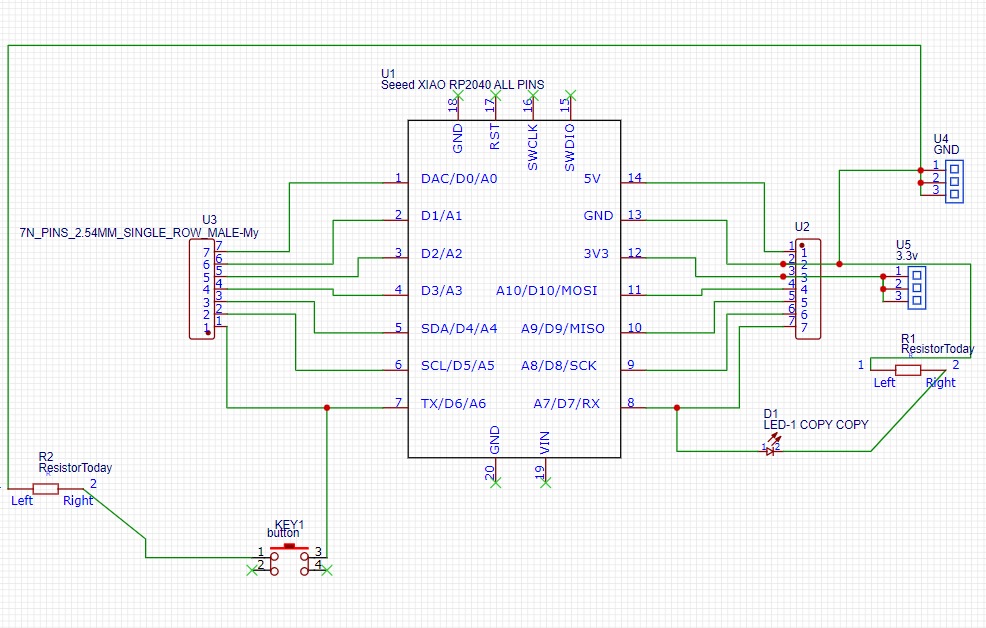
I used RP2040, ultrasonic sensor and male header pins.
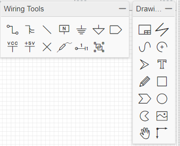
Once I imported all the necessary components, it was time to connect the wires in the schematic. You can do that using the top right panel in the interface as shown in the figure below: Tip: Make sure to mark x on the ports that are not going to be connected to anything or it will show as an error.
After all connections are made it looks like this:
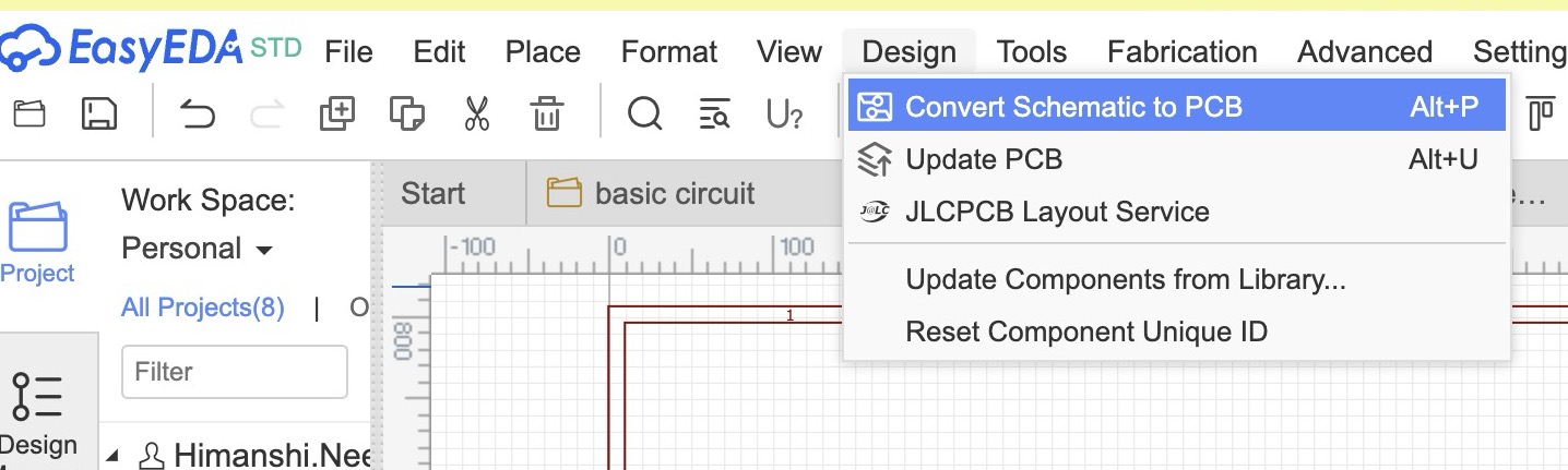
Once all the connections are done, we conver the schematic into PCB design. The steps are Design > Convert schematic to PCB.
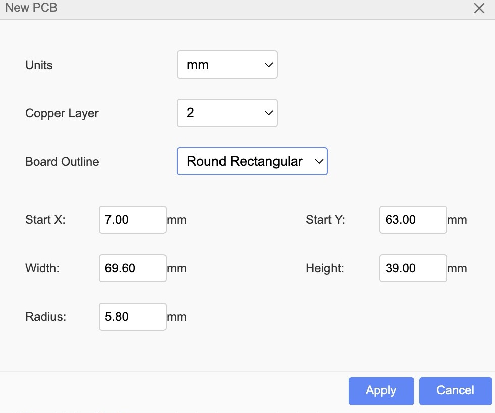
You can check nets before converting when the dialog box pops up. Once that is done, the following PCB design dialogbox opens to choose the parameters. You can keep to default parameters as EasyEDA sets right parameters anywhich ways.
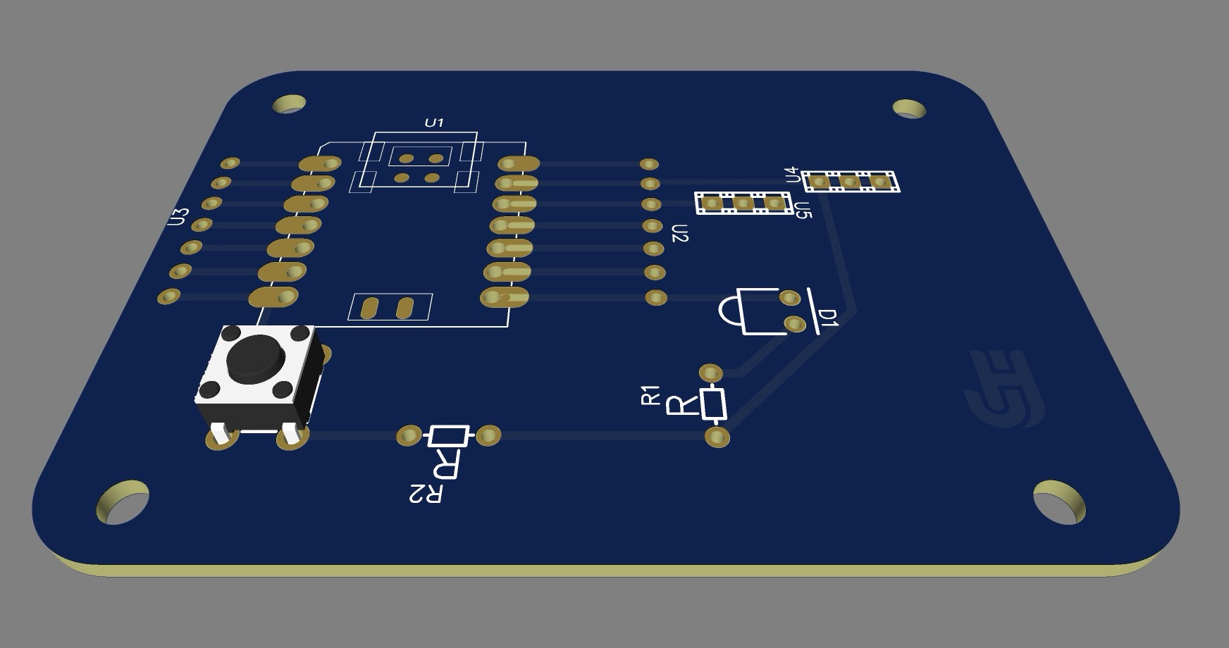
Now first we need to move all the components to the desired locations on the board. The standard board shape from the software is a rectangle as seen above. But we can design whatever shape we want.
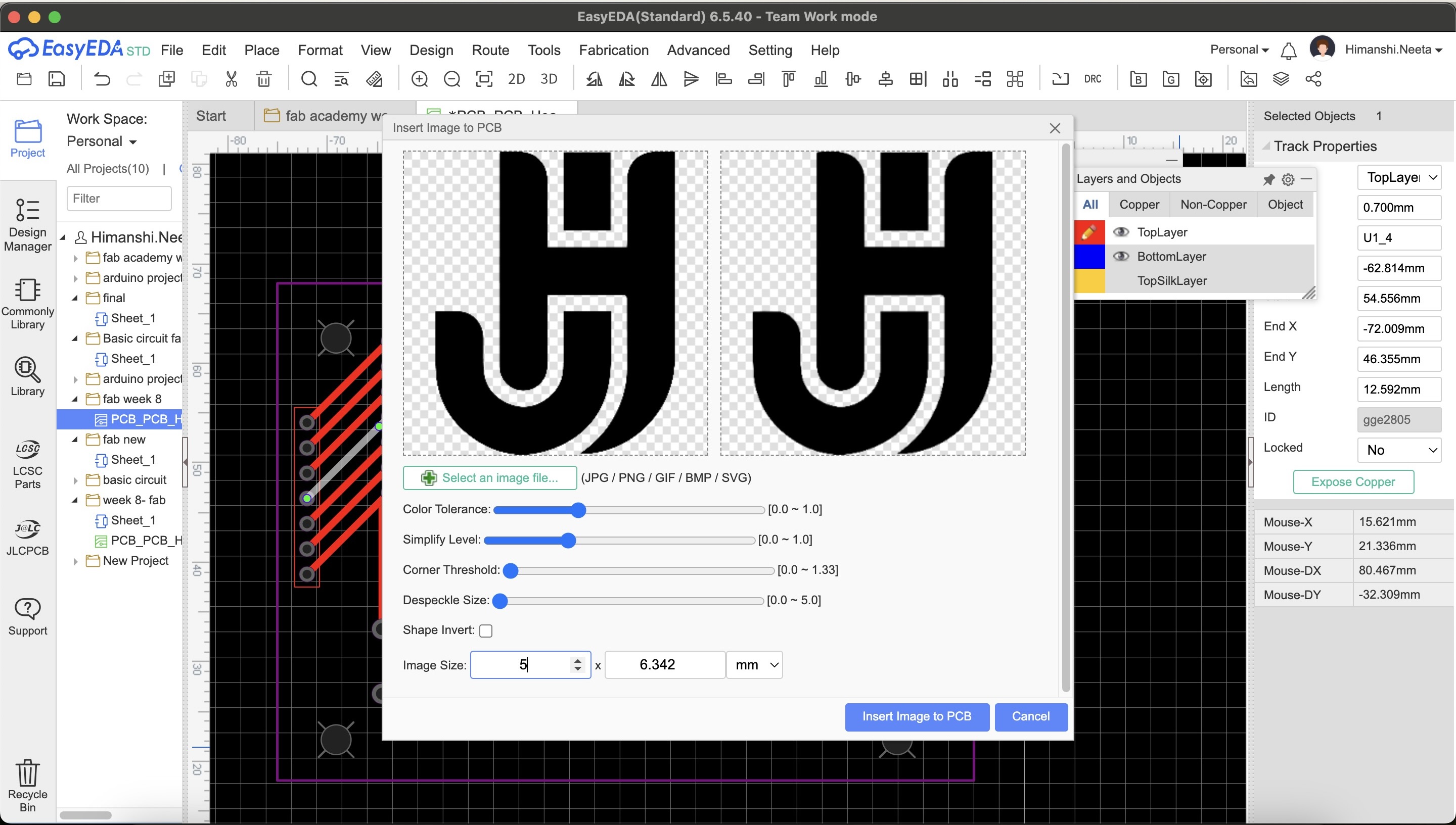
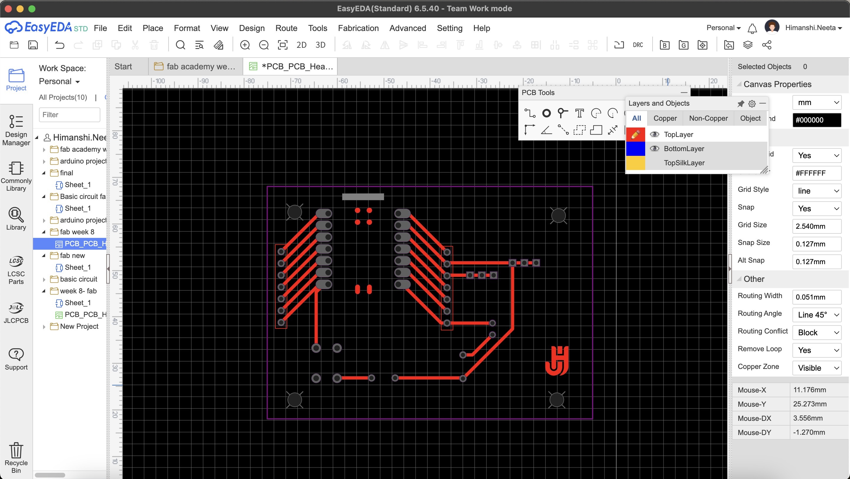
We can also add images on the PCB like our logo or any other image, I have added my logo to give my PCB a personal touch.
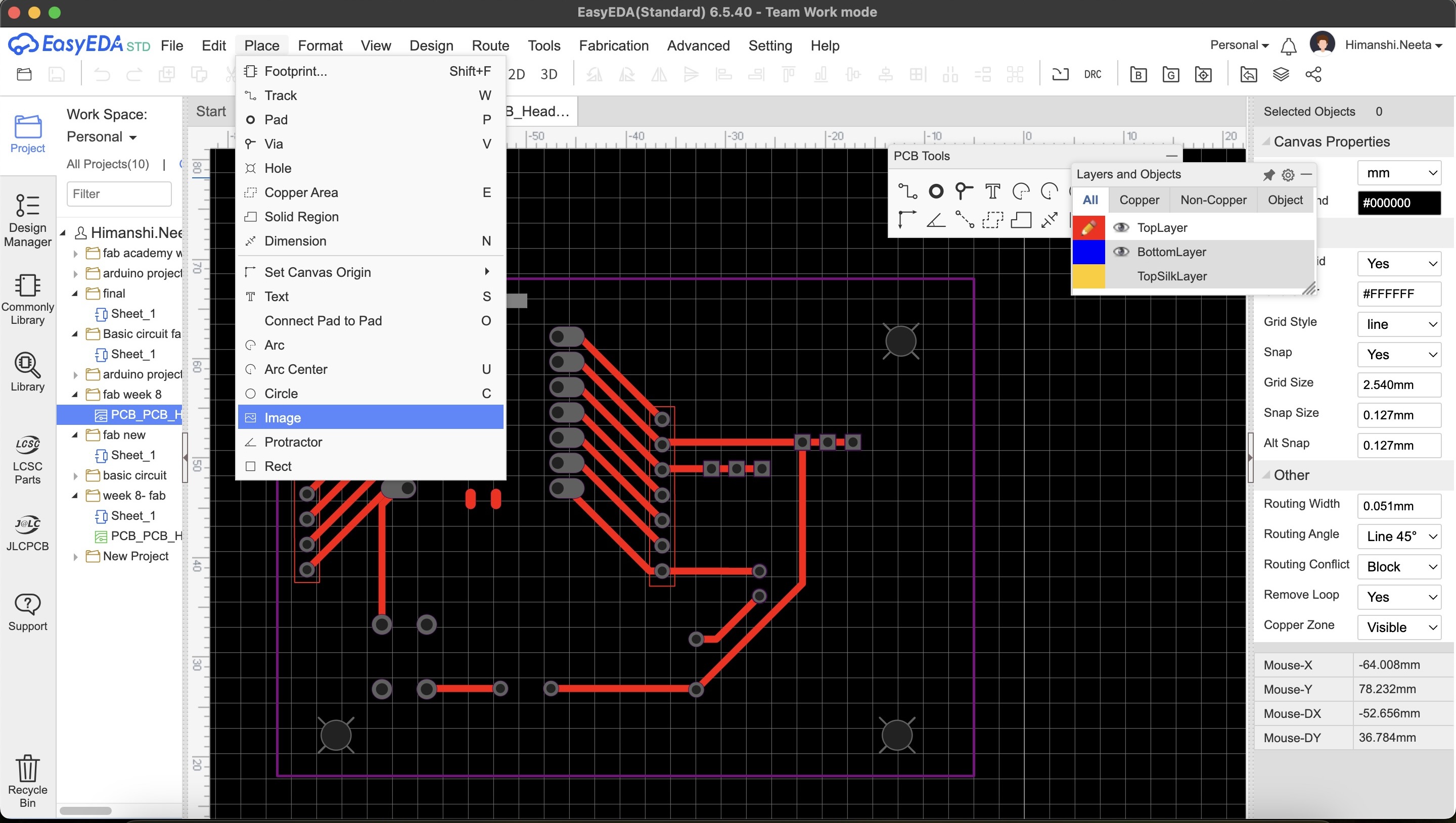
To select image go to:
Place > Image
You can adjust size according to your PCB and where you want the logo.
This is how it looks after placing the logo
For mounting purpose of our PCB, we can add holes and also edit the size, etc as shown below:
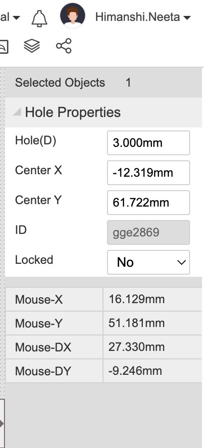
This is how it looks after mounting
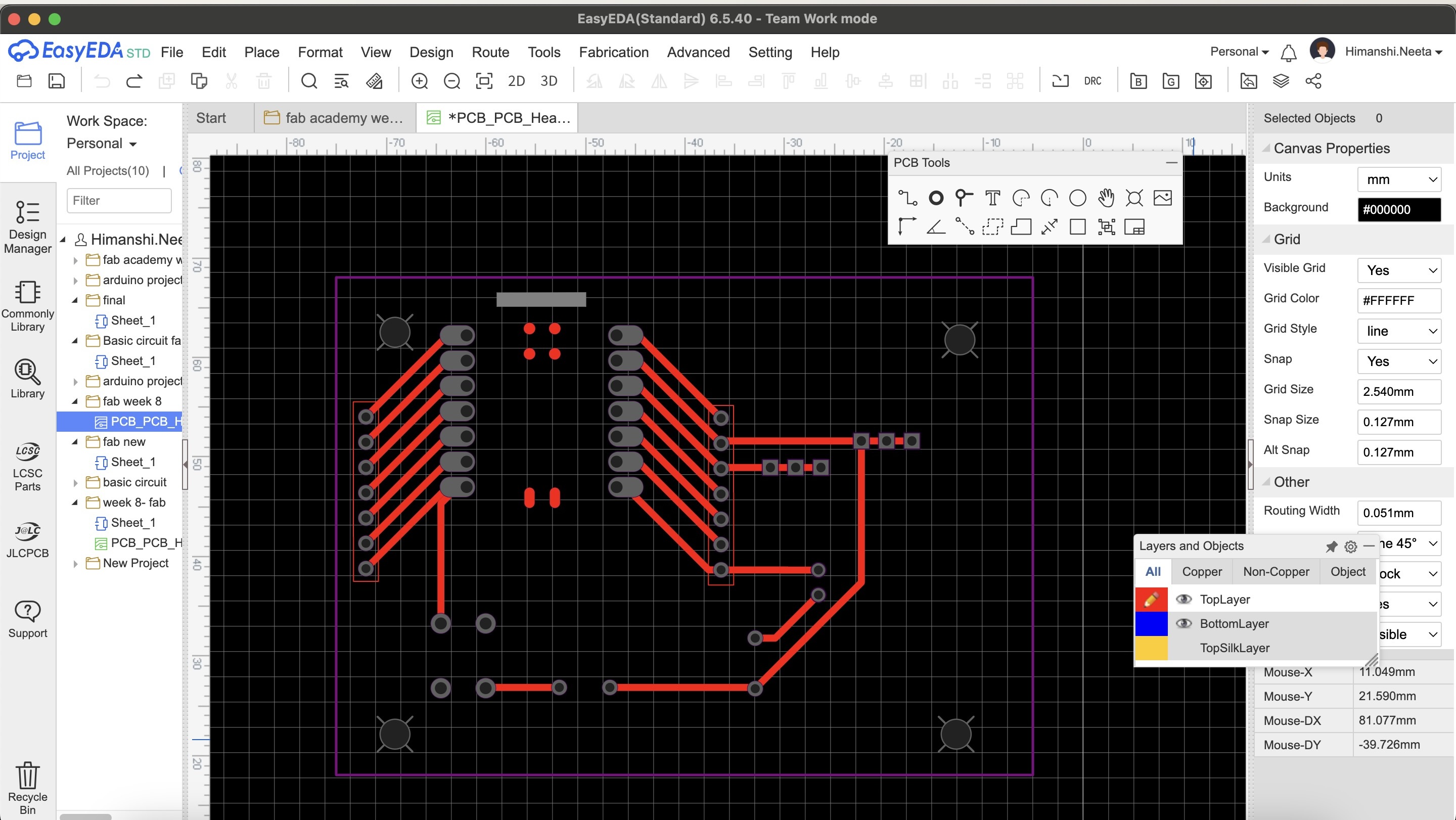
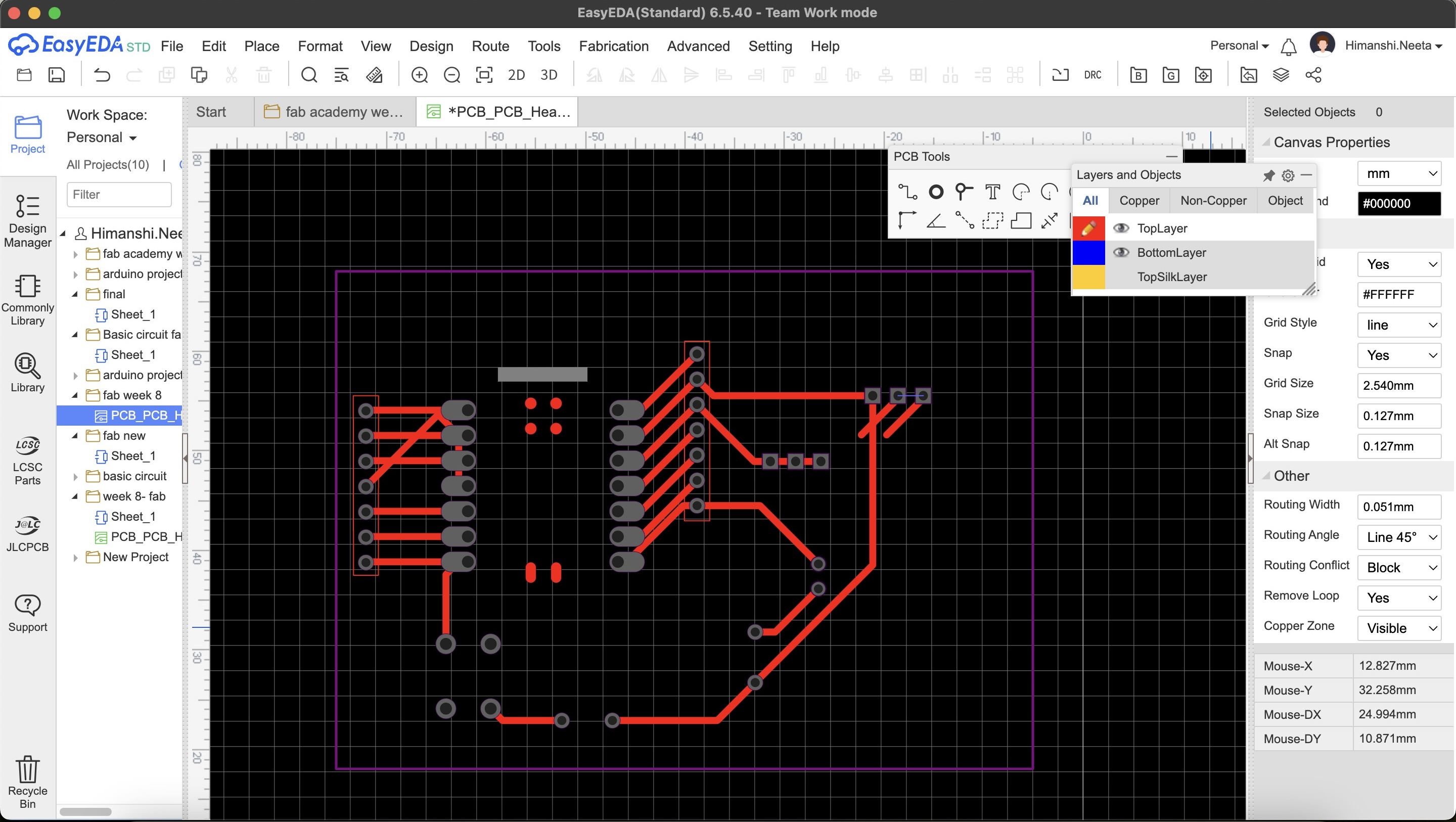
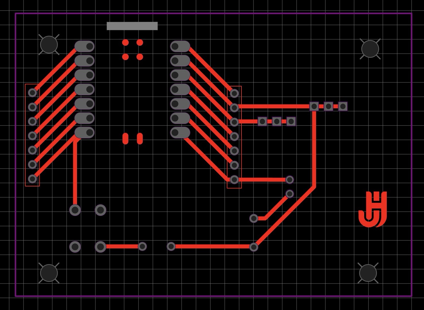
Now next step is to arrange the components in the desired positions on the board and then route the wiring.
For routing the connections, we need to know the design rules for the same. Here's the dialog box and the settings you should ideally use.
Design > Design rules > Setting
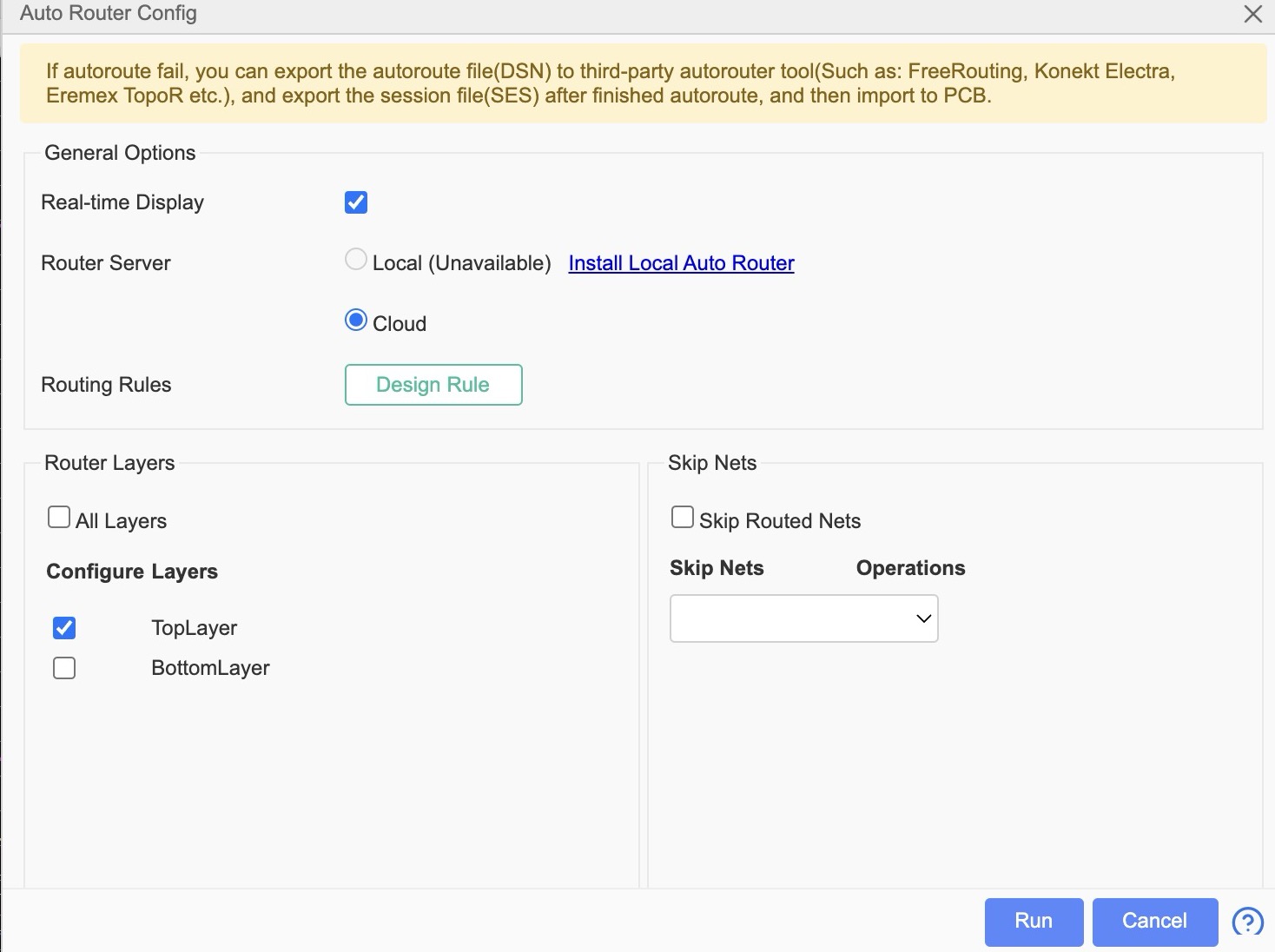
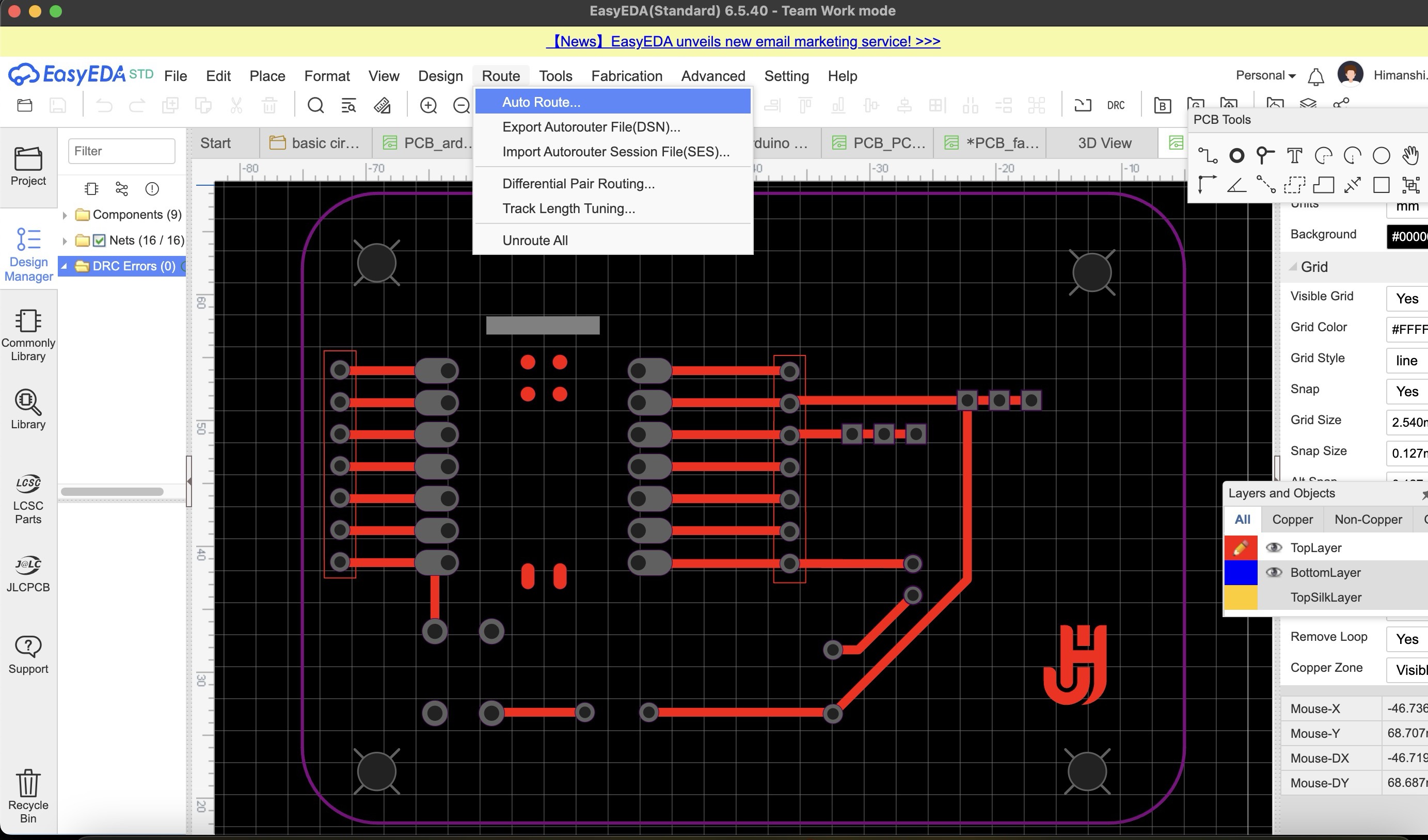
Actually, ideally for a ground connection, you should just have a plane, but since this is just 5V circuit and a simple one, 0254mm width ground line should also be fine. While you can manually connect using the wiring option, there is a auto route option in EasyEDA as shown in the figures below:
In the above image I unticked the bottom layer and skip routed nets.
ROute > Autoroute > Run
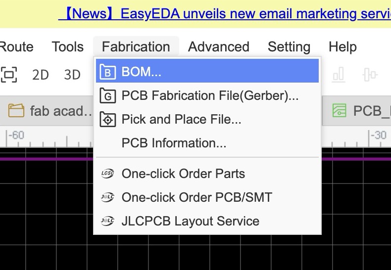
EasyEDA also generates BOM that can be used to order the components quickly or if we are ordering the PCB directly from the JLCPCB, then check for availability.
Fabrication > BOM > Export BOM
Next step is to do DRC check that is Design rules Check from the software end. It is very important to do this before you export your Gerber files. If we have any node open, or any connection incomplete, this check points out those mistakes.
Design > Check DRC
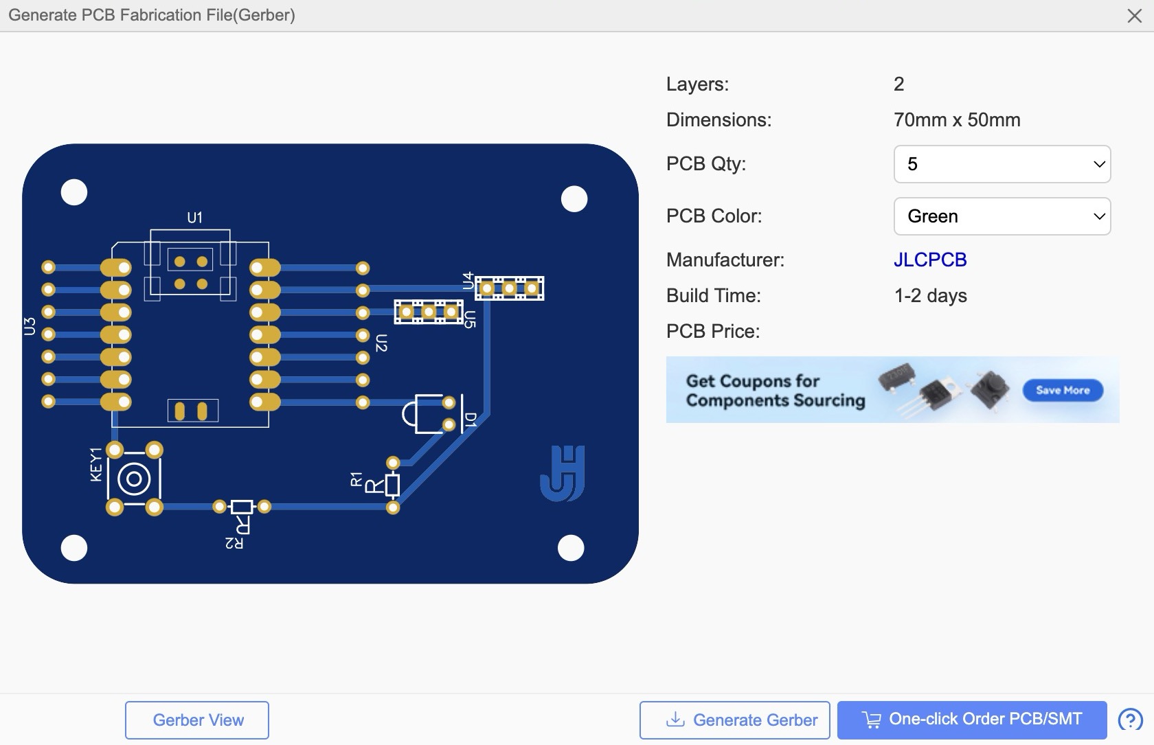
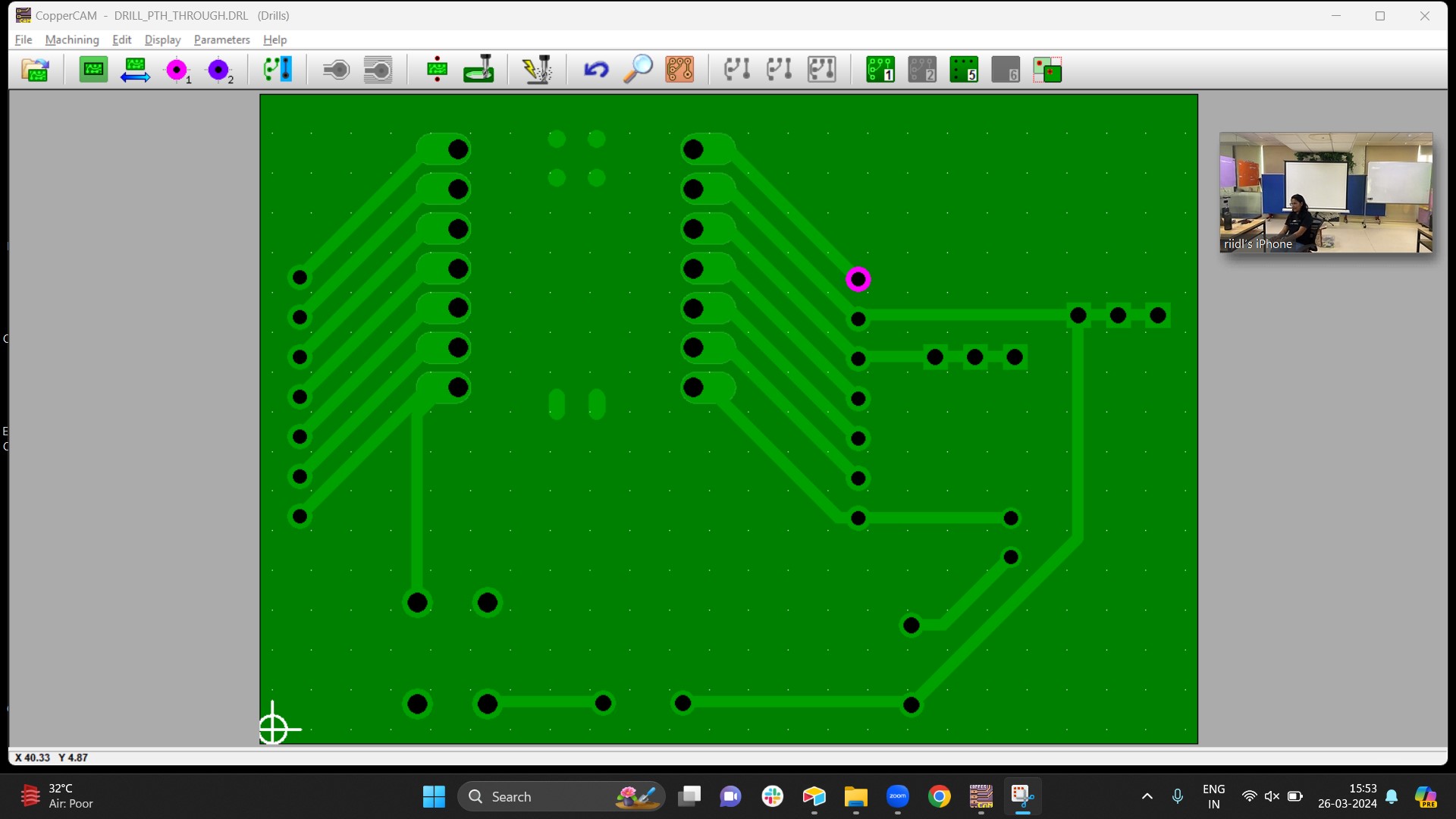
Last step is to download Gerber files, which are needed in the next software for PCB milling.
Fabrication > PCB Fabrication file Gerber > Check DRC > Generate Gerber
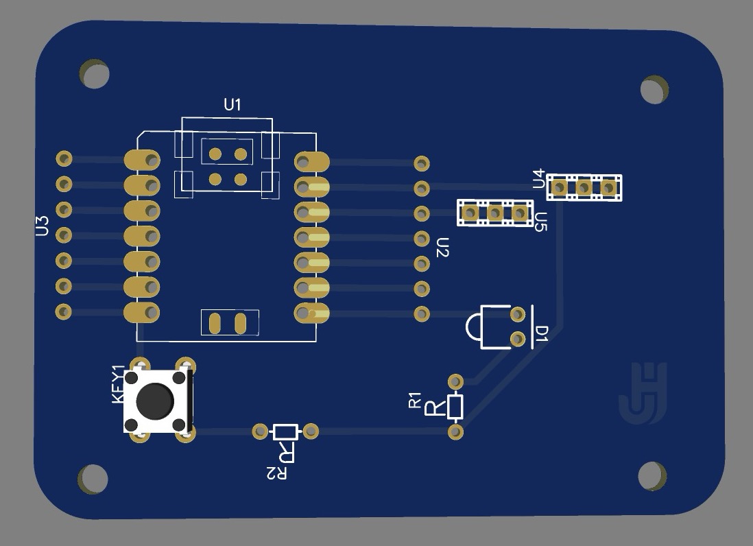
In EasyEDA, you can also visualise the 3D view of your PCB after assembly, provided you have chosen the right components from the library back during the schematic design time and those components had a 3D view uploaded in the library. Just click on the 3D option in the top toolbar. So these below are the 3D views of the 2nd and 3rd iterations of the PCB.
Milling
Once the PCB file is ready I started with milling the PCB. Here are the steps for the same
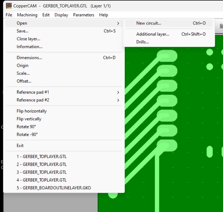
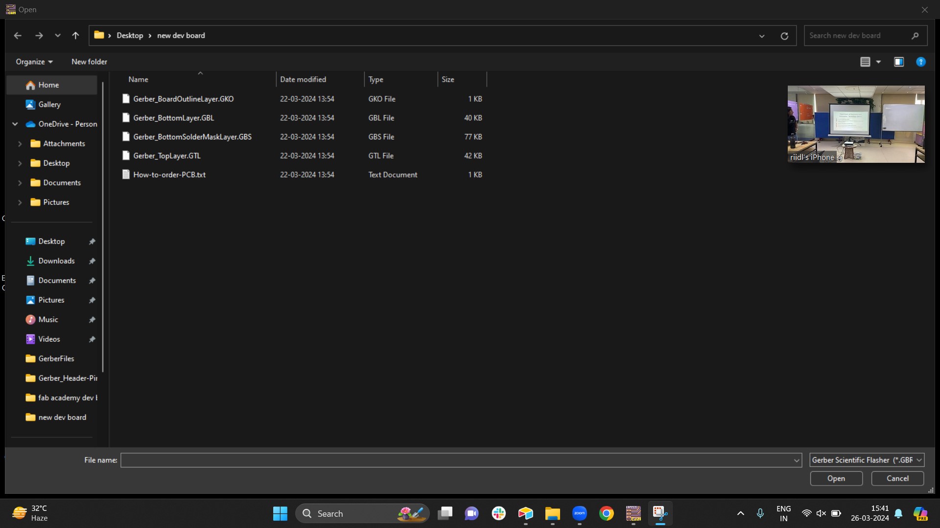
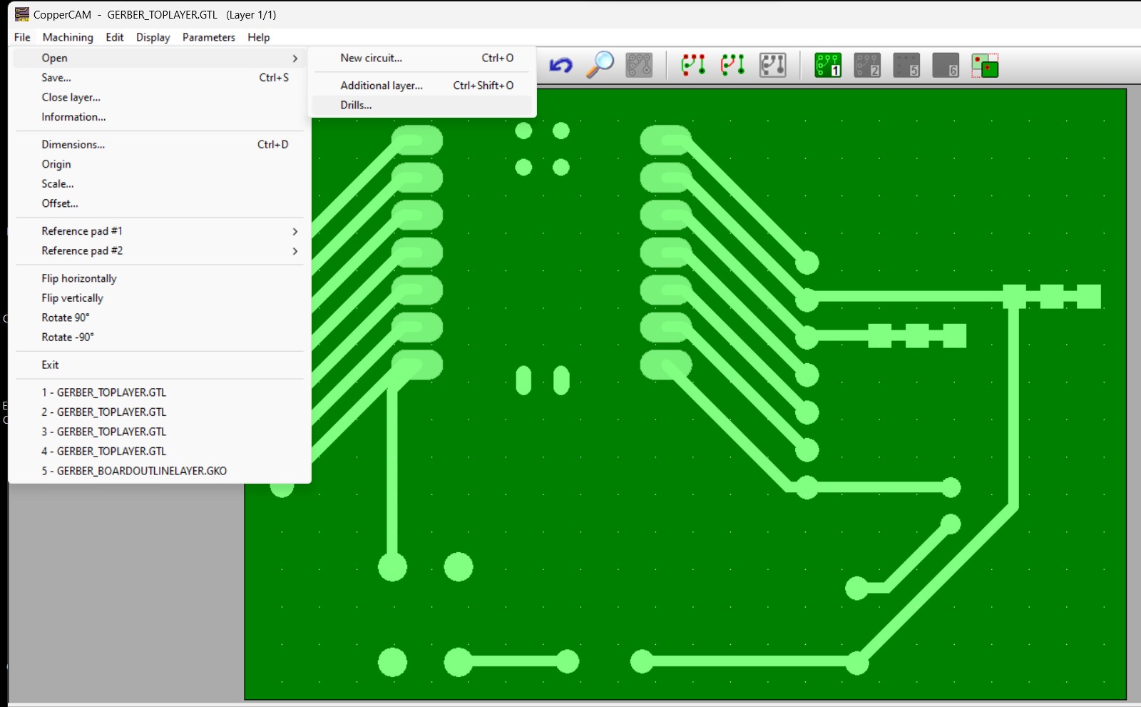
At the start import your file:
File > Open > Select your file > Top layer
Board outline layer will be selected later, as we did not have bottom layer and bottom solder mask layer we didn't selected that
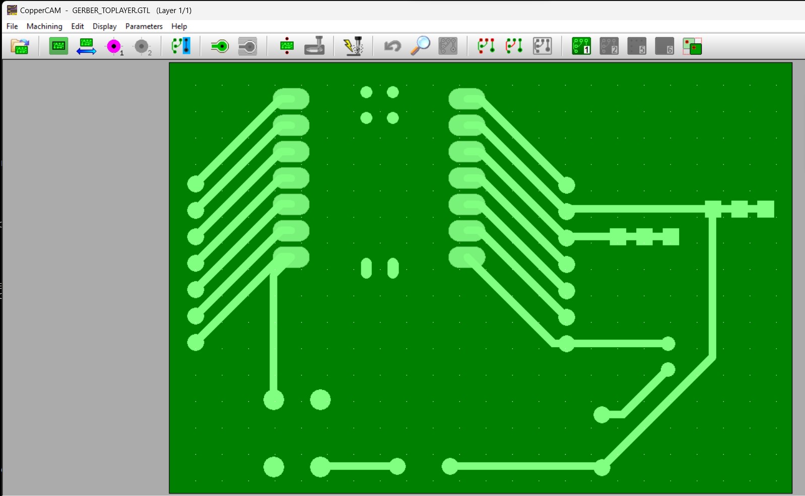
This is how it looks after importing the file
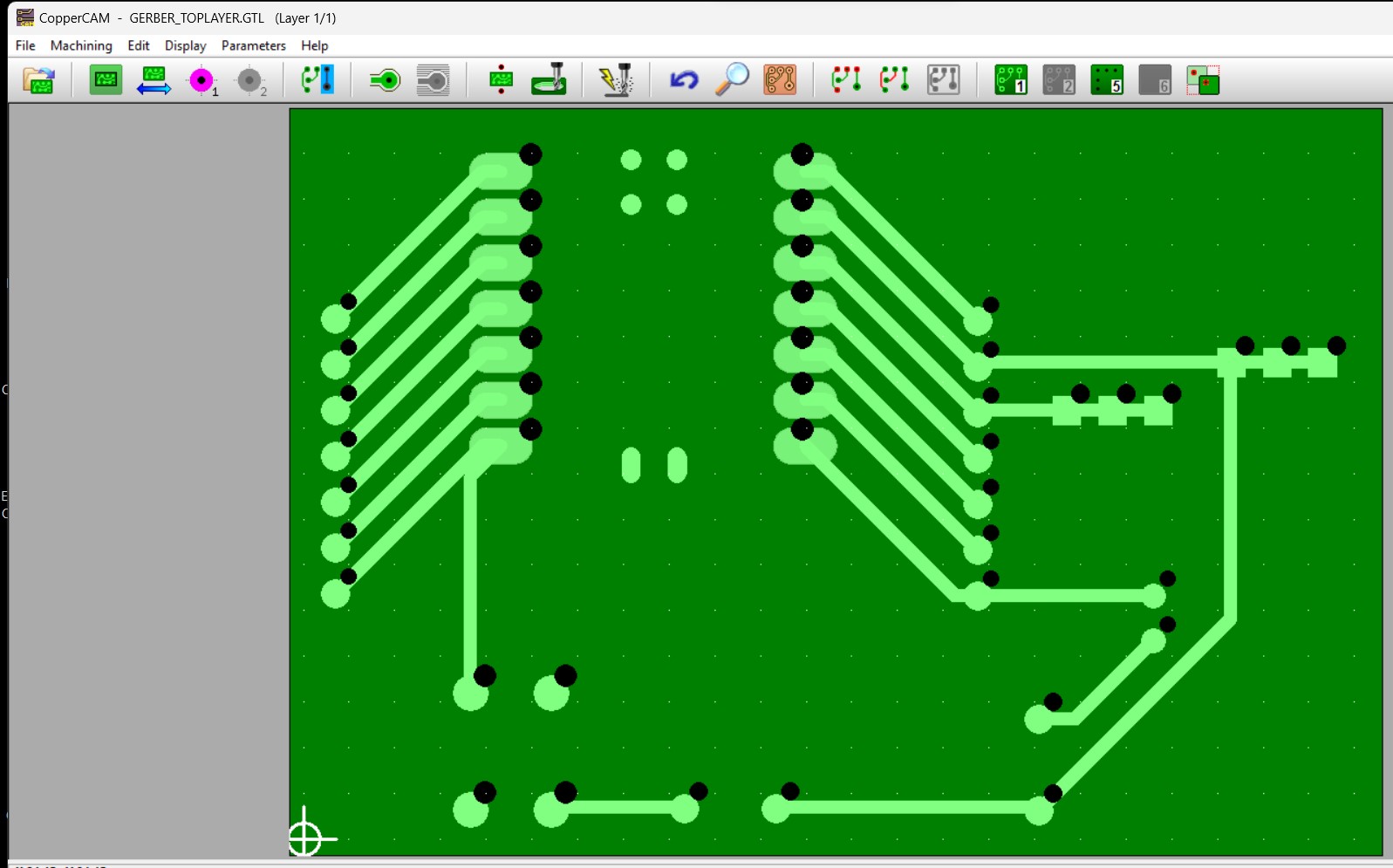
Now repeat the same steps and add drill layer and this is how it will come after importing
Now we need to allign the drill layer with top layer
Select drill layer (5) > Right click > set as origin > again right click > Set reference pad
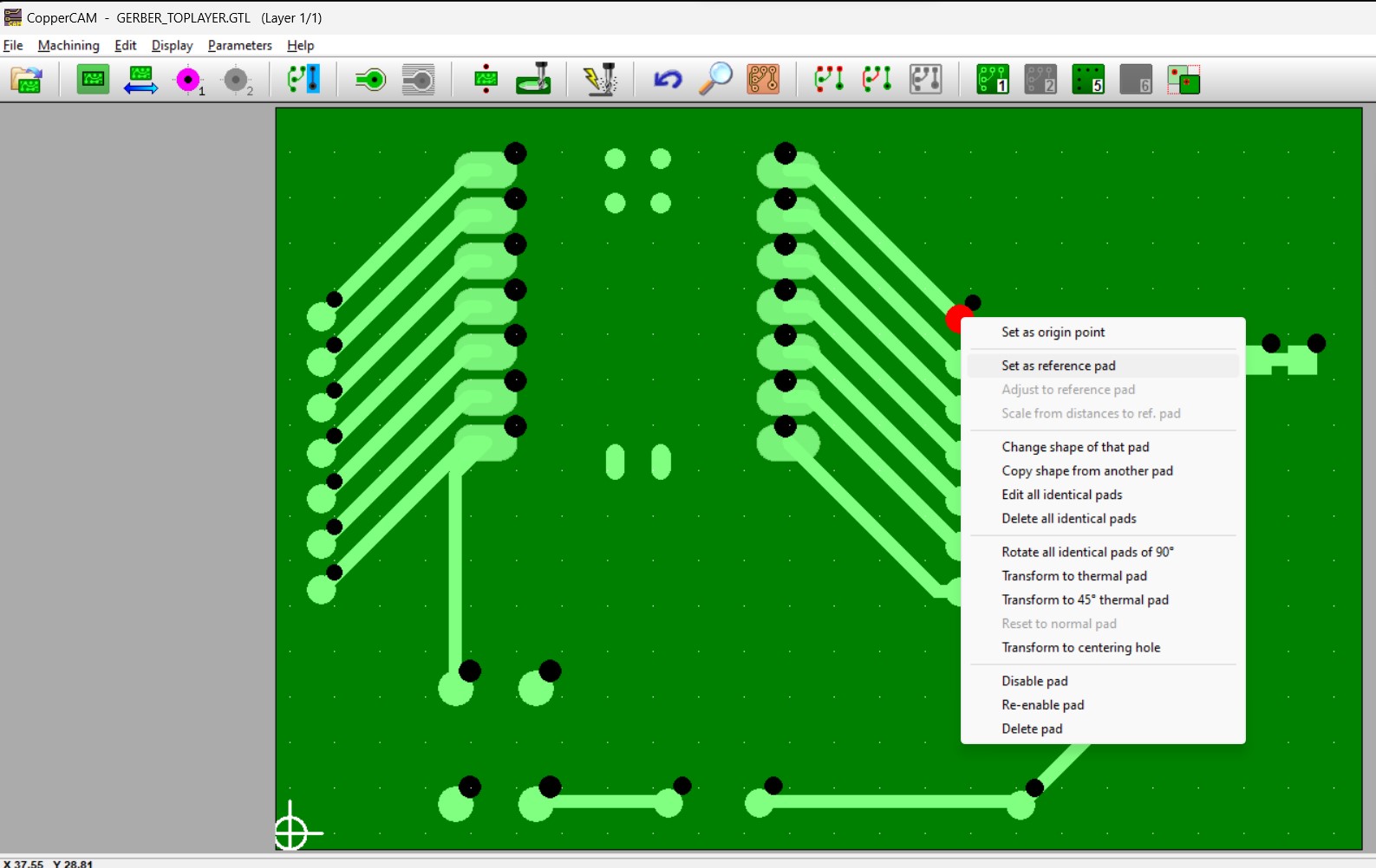
Now select drill layer:
Right click > set as origin > Again Right click > Adjust reference pad
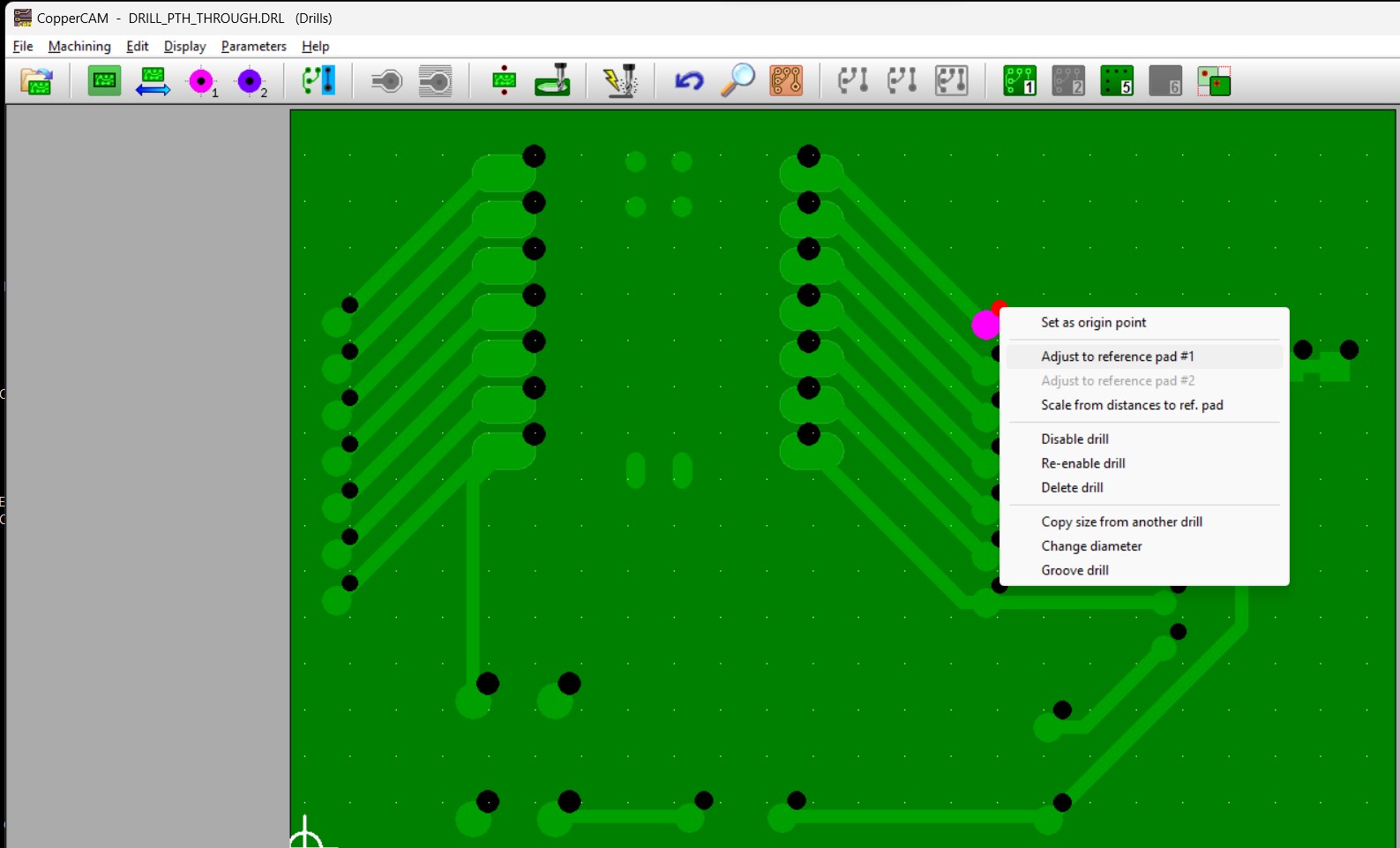
This is how it looks after alligning
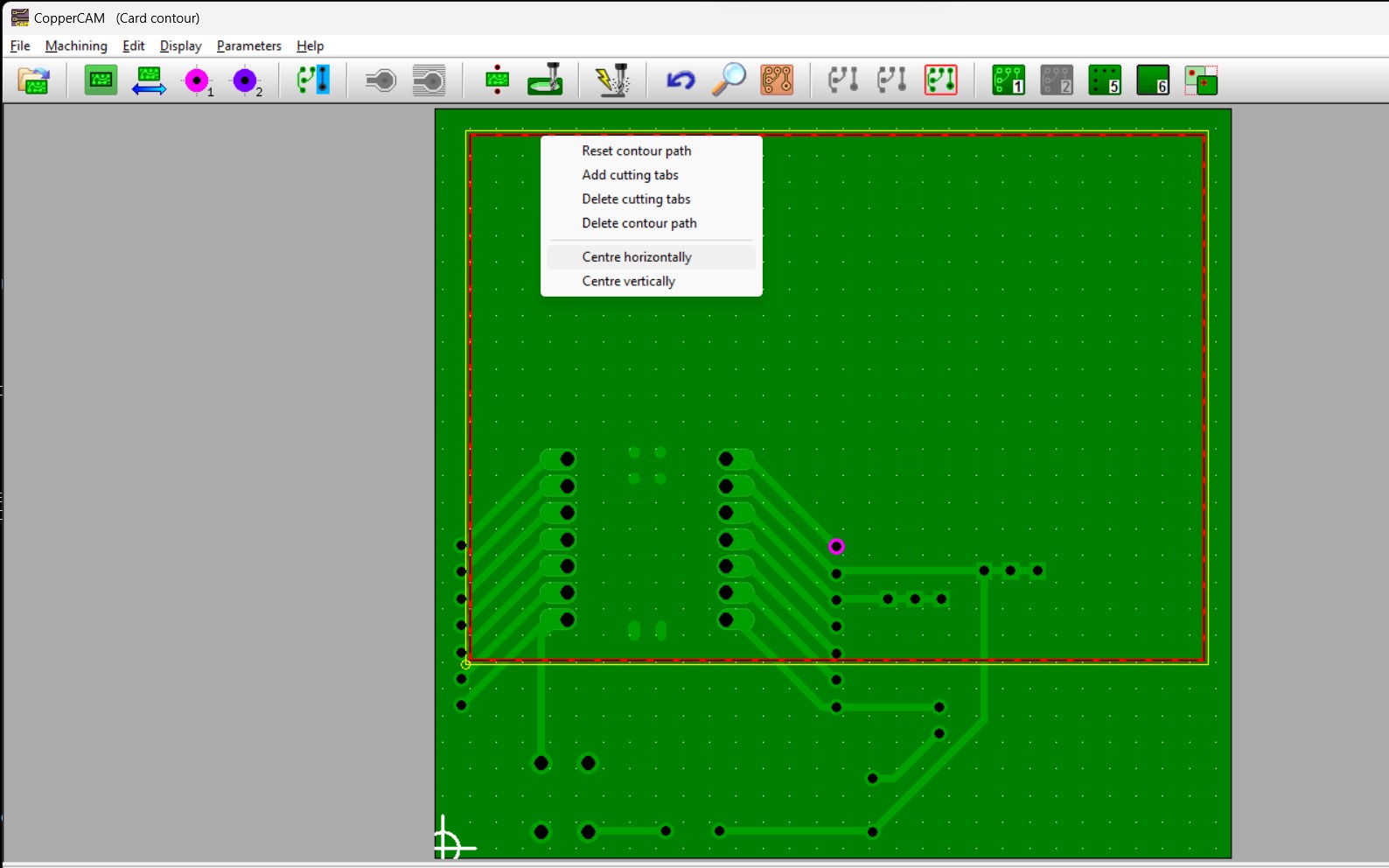
Now repeat the same steps and select board outer layer it should automatically go in layer 6
You can see numbers from 1 and 2 they are the layers. Layer 1 and 2 are for one sided PCB, 3 and 4 are for double sided PCB ,in this machine we cannot do 2 sided pcb, the 5th one is for drilling holes and 6th one is for outer line.
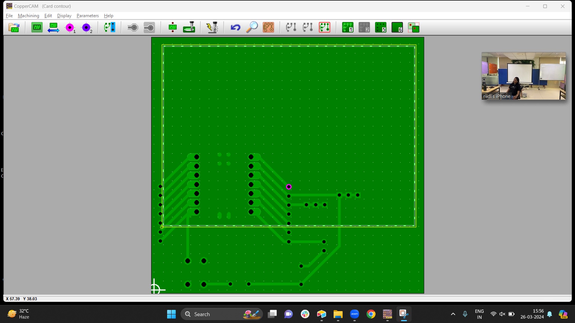
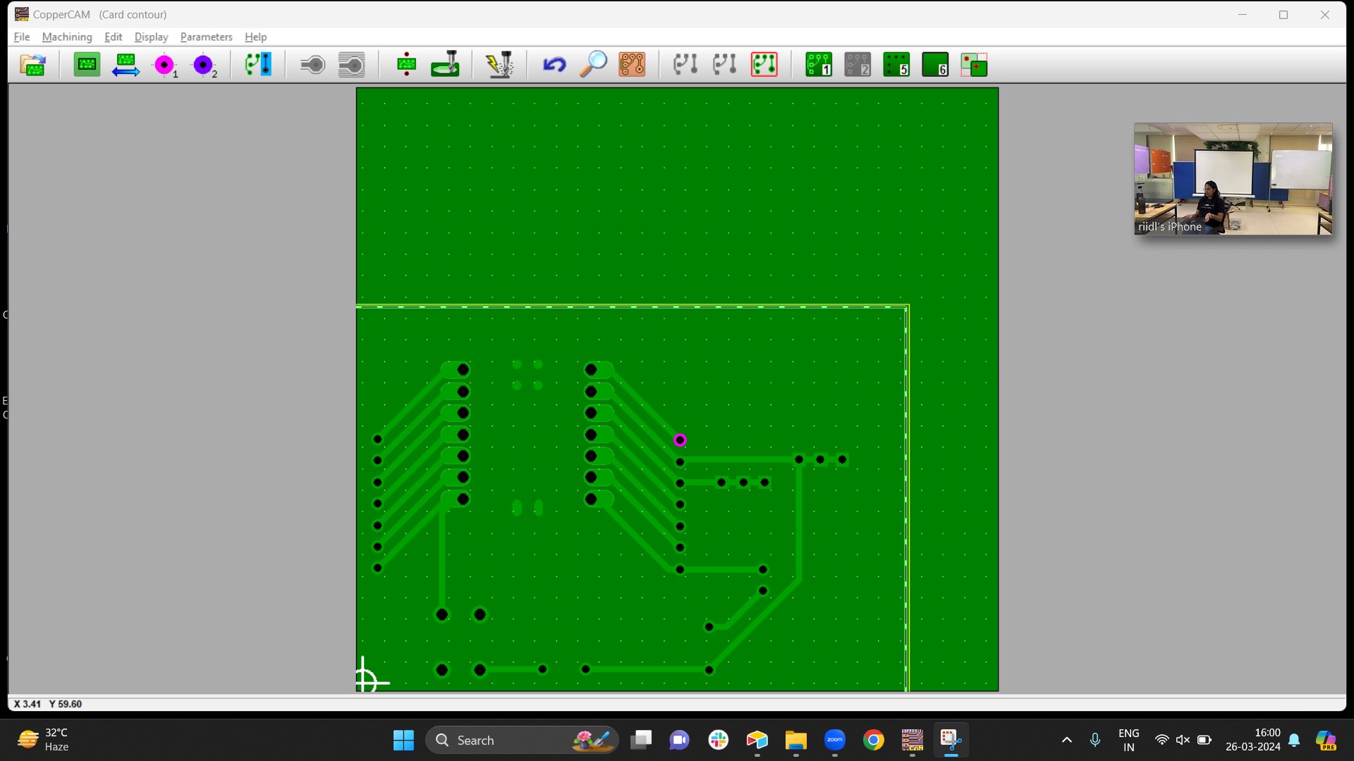
For alligning the outer box with the other layers :
Select outer layer > allign horizontally
Again Select outer layer > allign vertically
For engraving we use 0.8 conclave tool and for cutting and drilling holes we use 0.2 conclave. If we don't have any tool we can add it from tool library, every tool has a fixed parameter so whatever tool we are adding we need to add it's parameter like diameter, profile, angle and so on.
Go to track apentures and put track width as 0.7mm, this we got after a lot f try and error as shown in Week 4
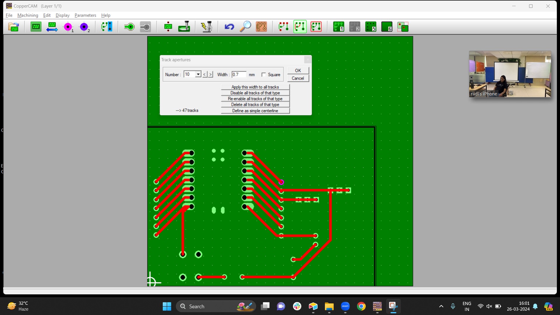
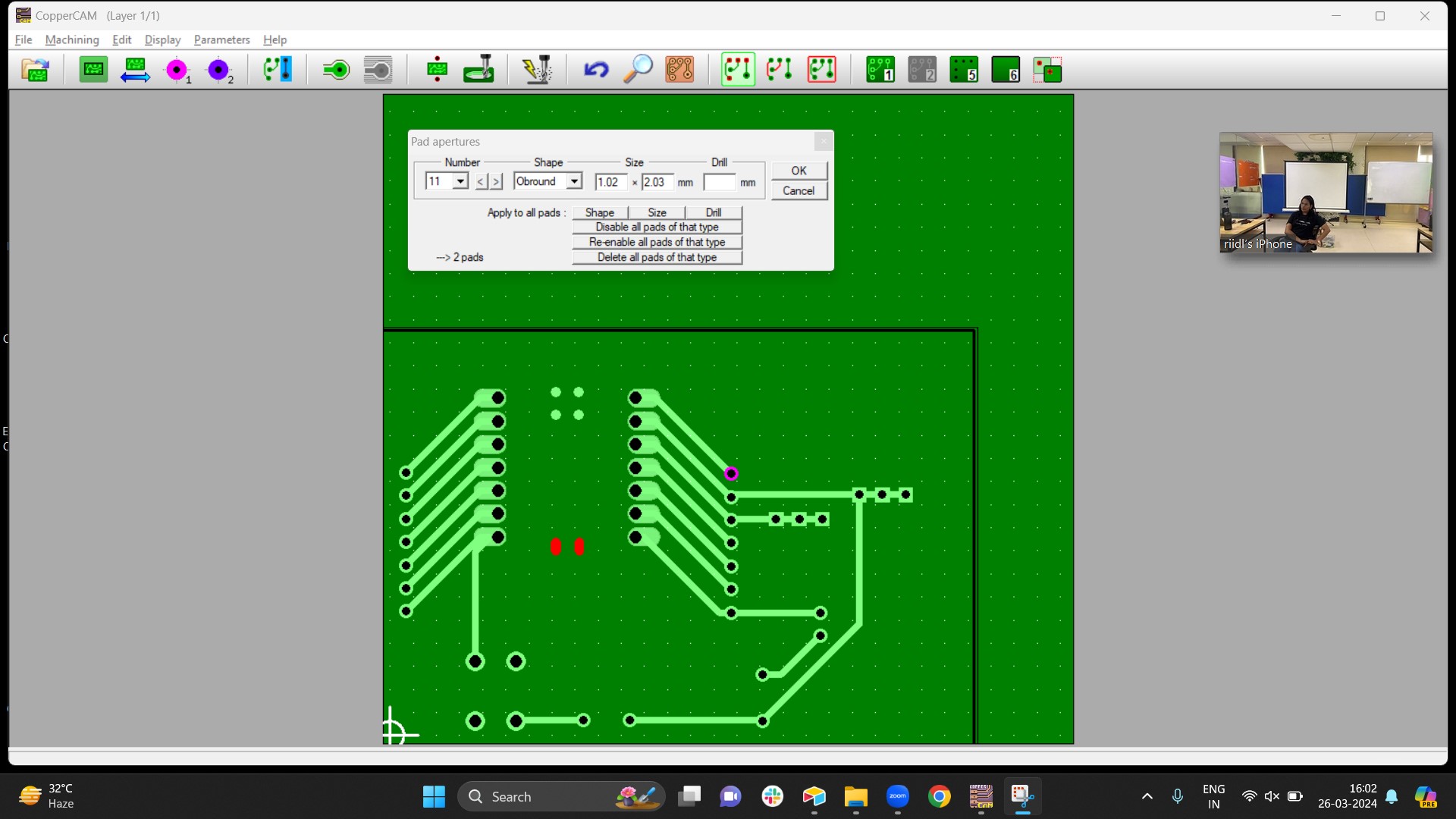
Now go to pad apentures and adjust pad width we kept it as 1.02 * 2.03
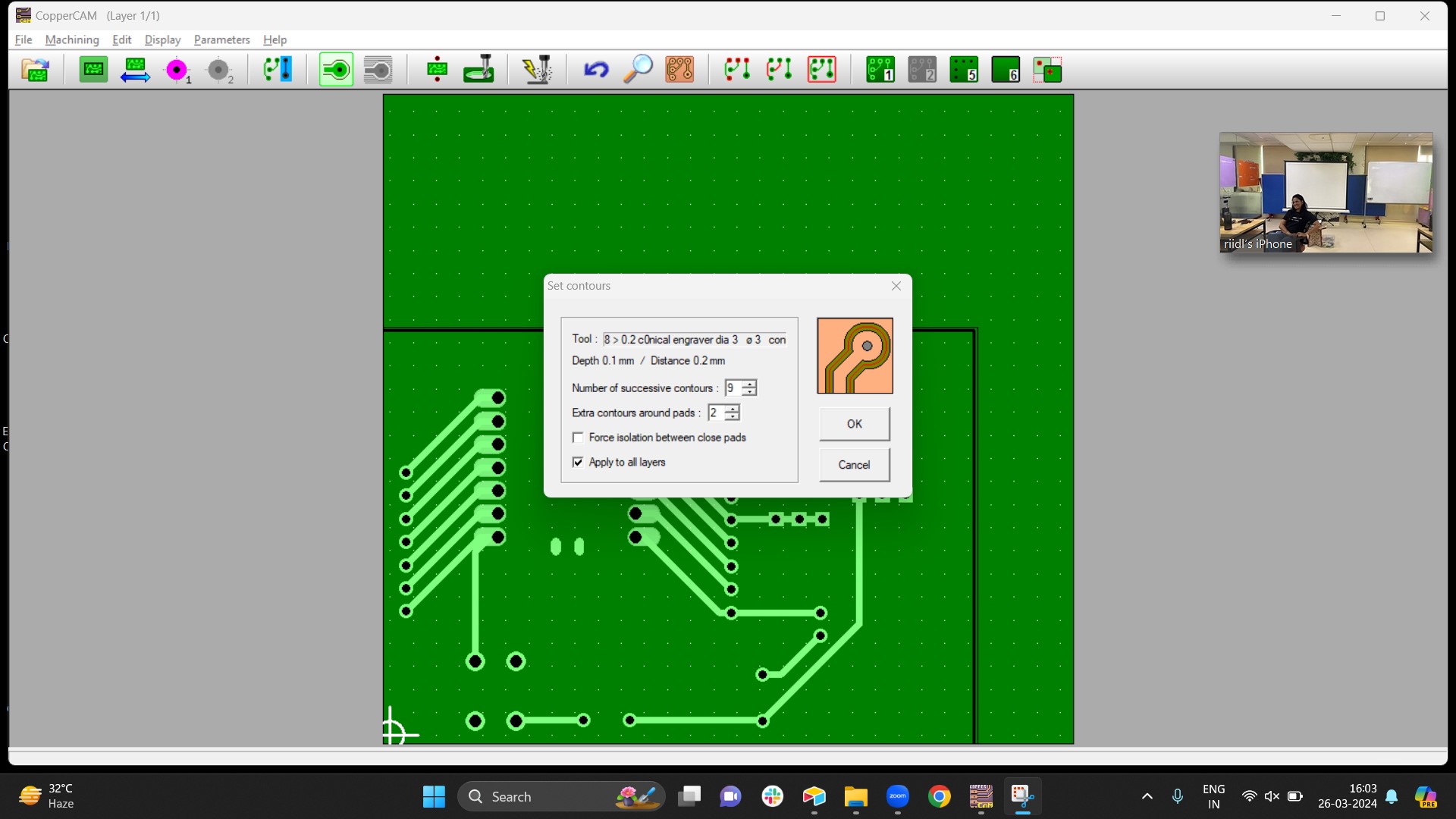
Now after preparing file go to calculate conteurs here you can see number of successive conteurs meaning how many times our tool will go on tracks and pads, set it as 2 because if it fails one time it can cut or engrave the 2nd time. Keep apply to all layers on.
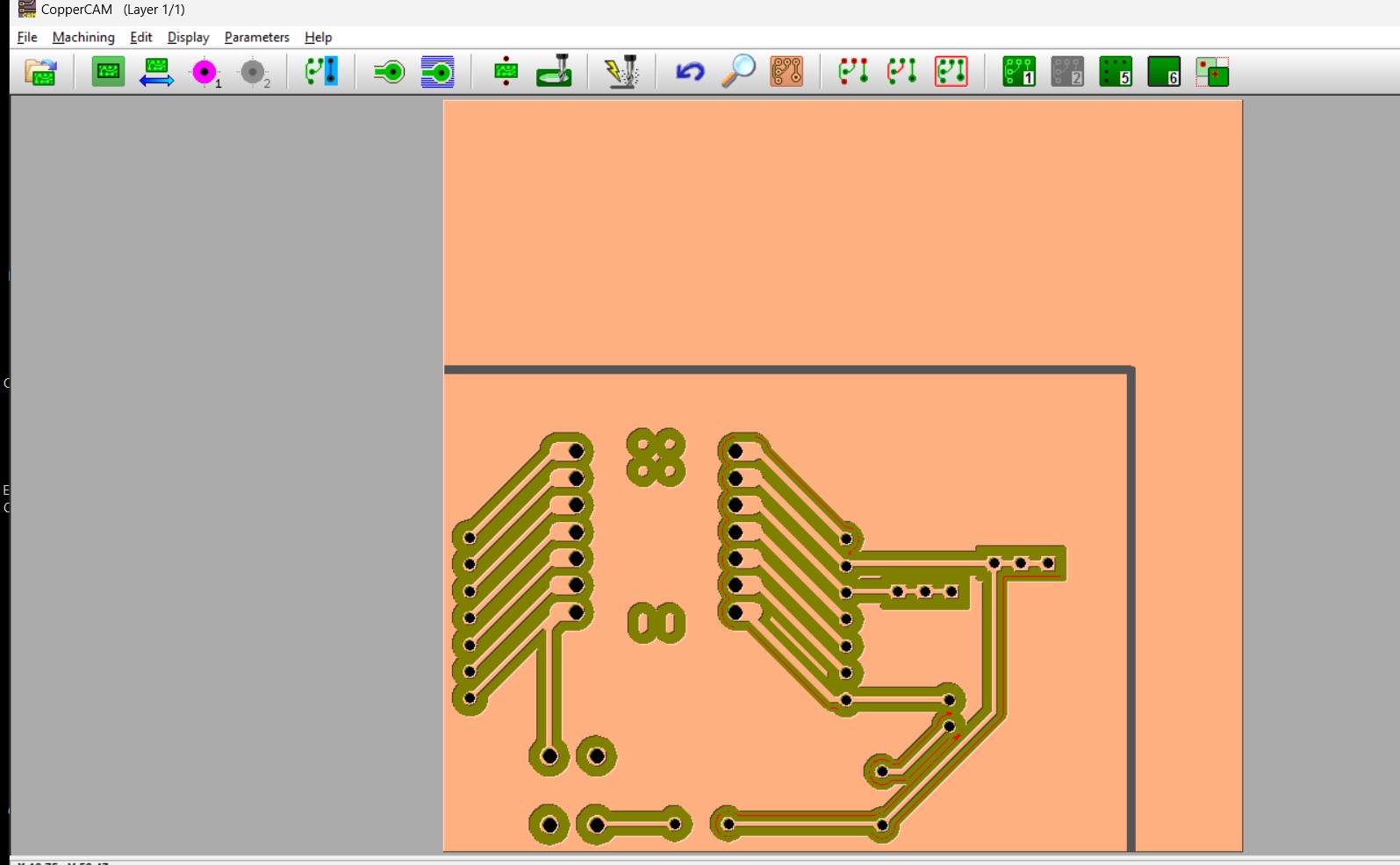
This is how it looks after all the above settings is done
After generating conteurs open output window, we normally do engraving first, so select that first
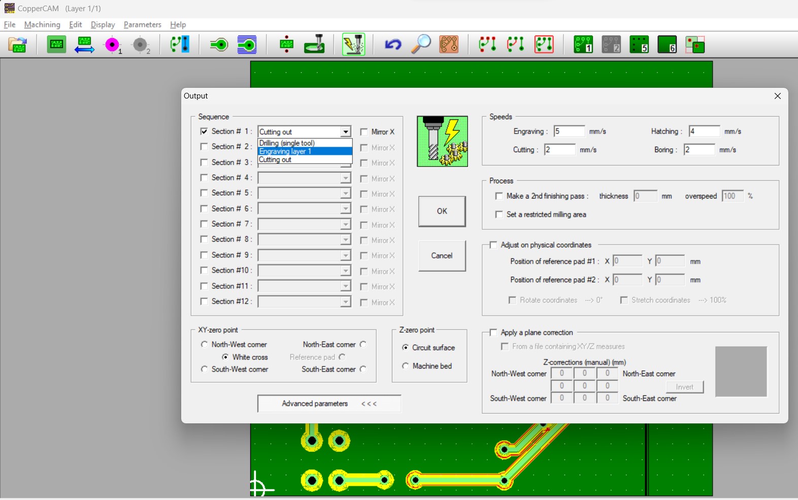
Now set your X,Y and Z axis in V-Pannel software
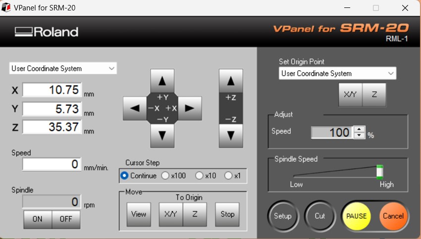
Then start milling a precaution measure drop down will open press continue to start.
Multimeter Testing
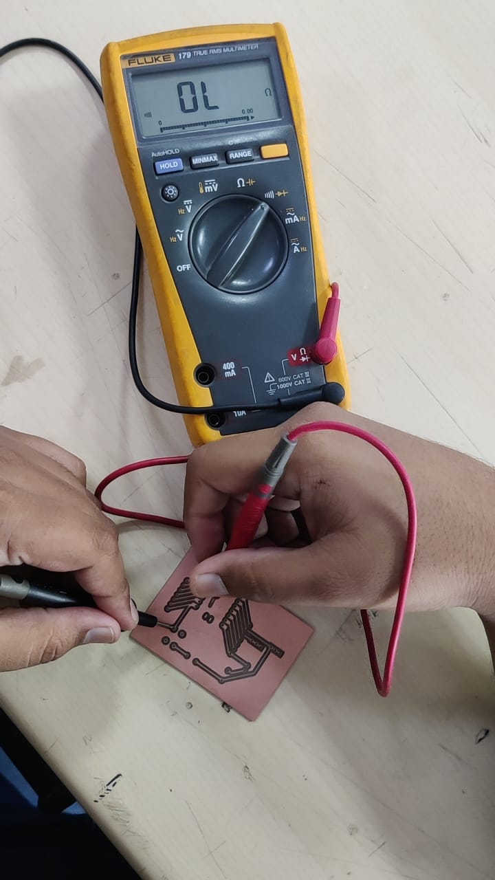
Before starting the soldering we did multimeter testing, There are 2 pen like structures called test probes which you need to keep on 2 connection and it beeps so if it beeps it means it is working and if it does not beep there is some error.
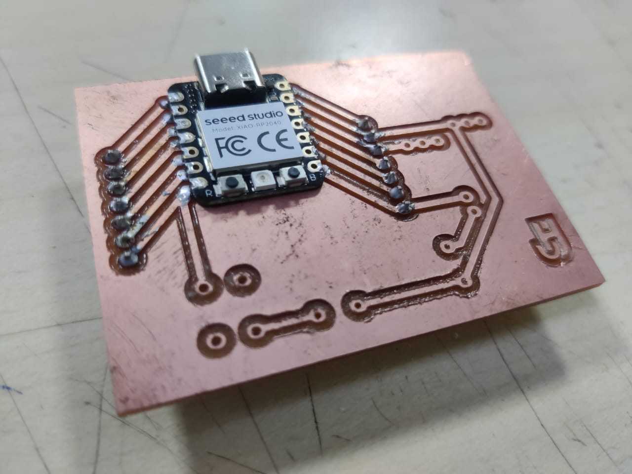
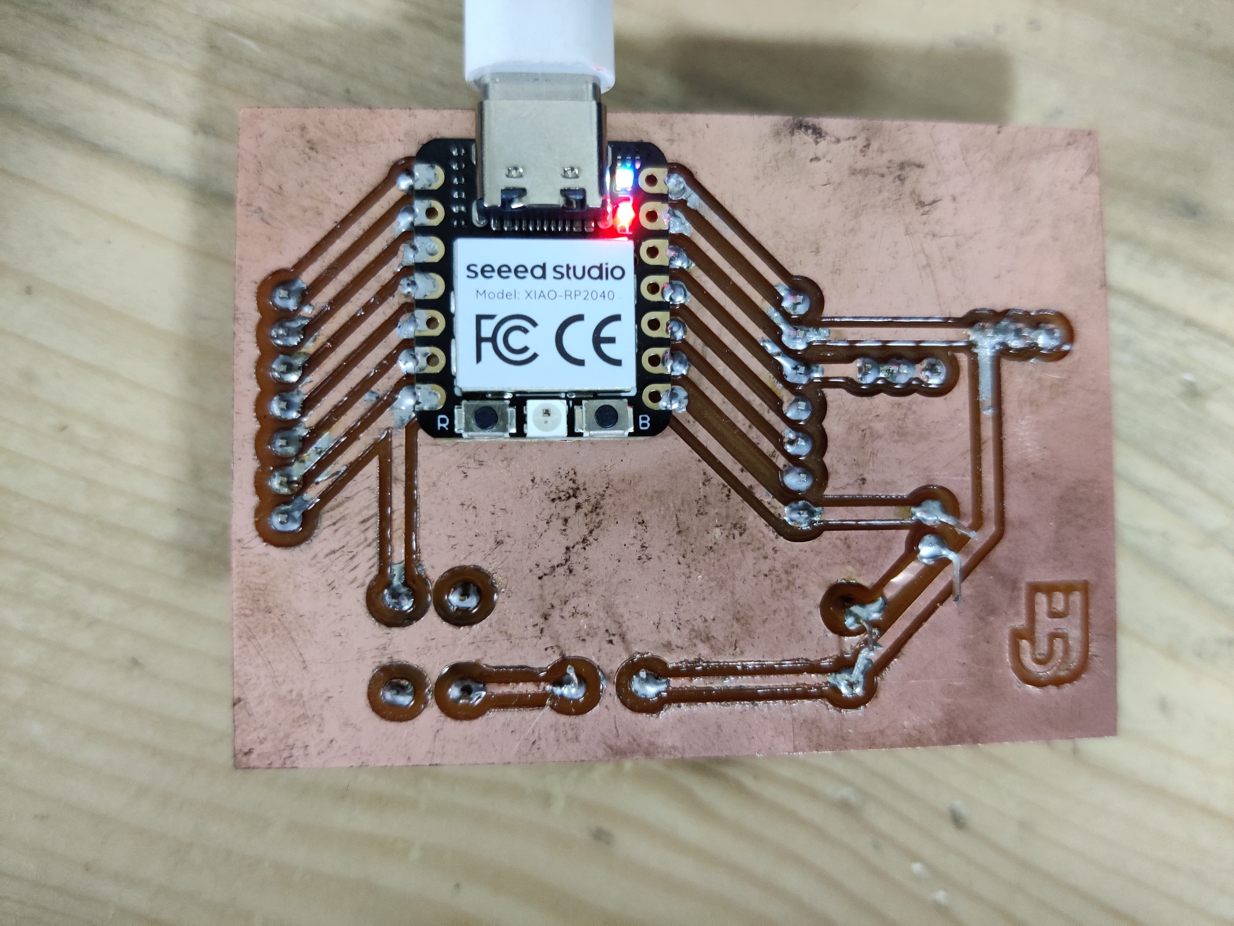
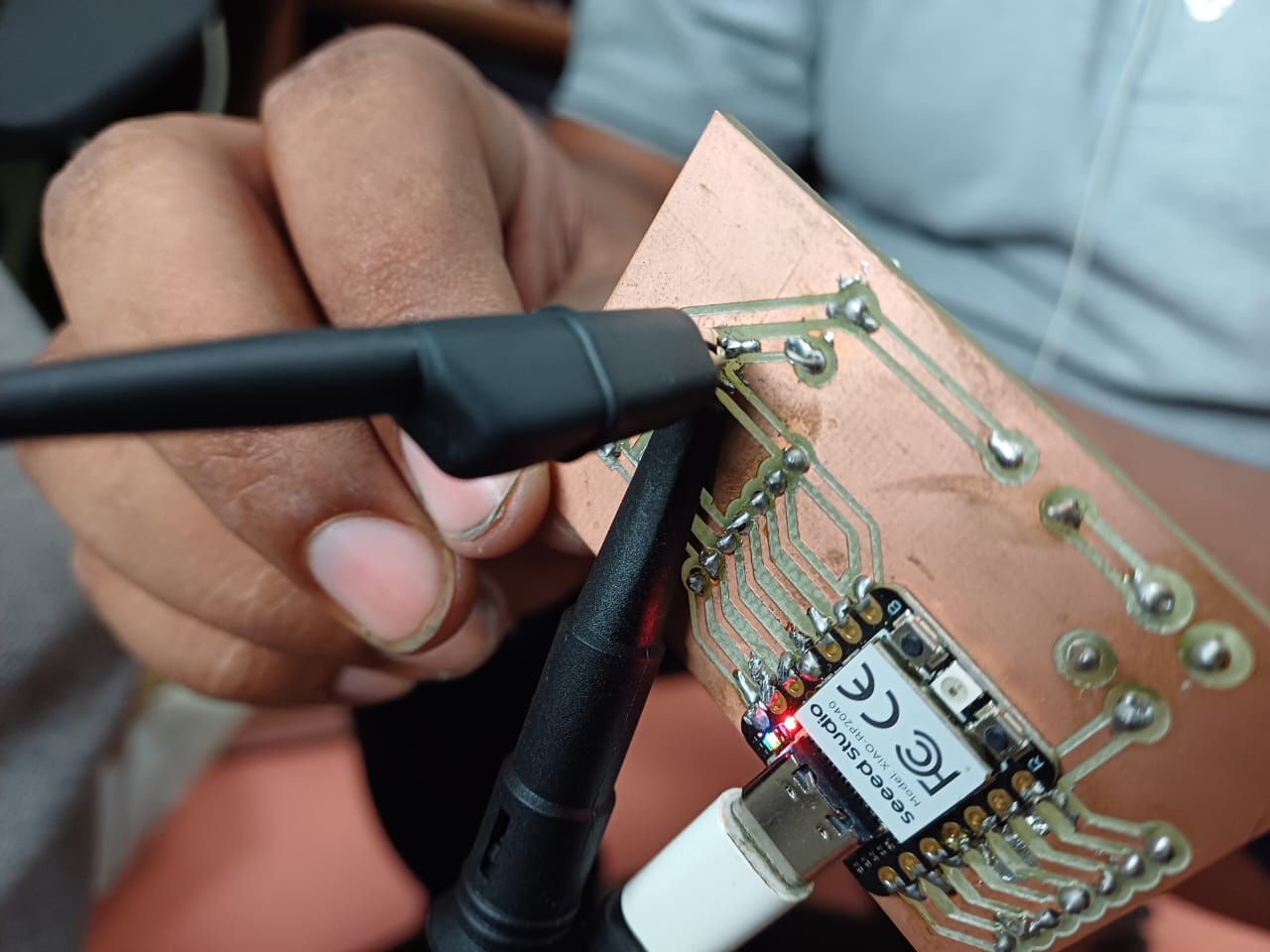
After Soldering
This was my first try of soldering the entire pcb and did not turn out good
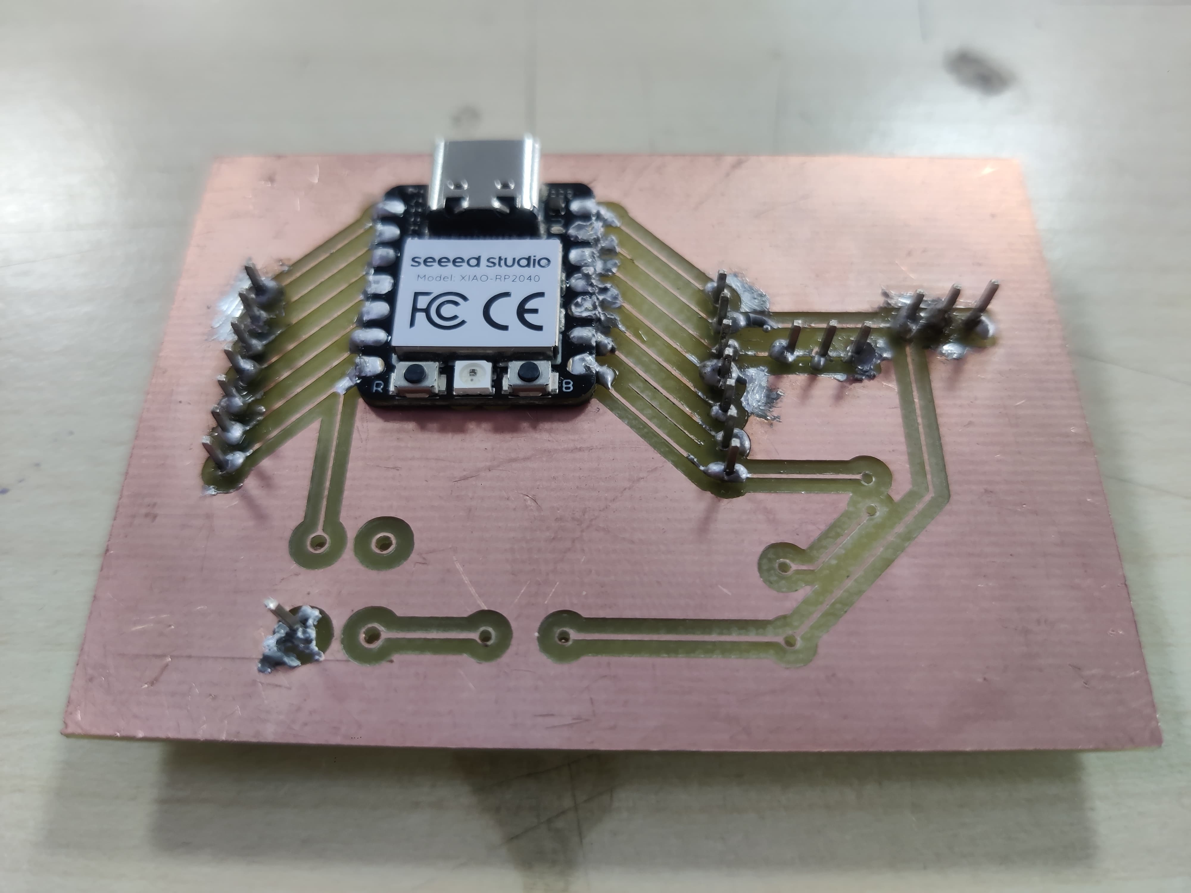
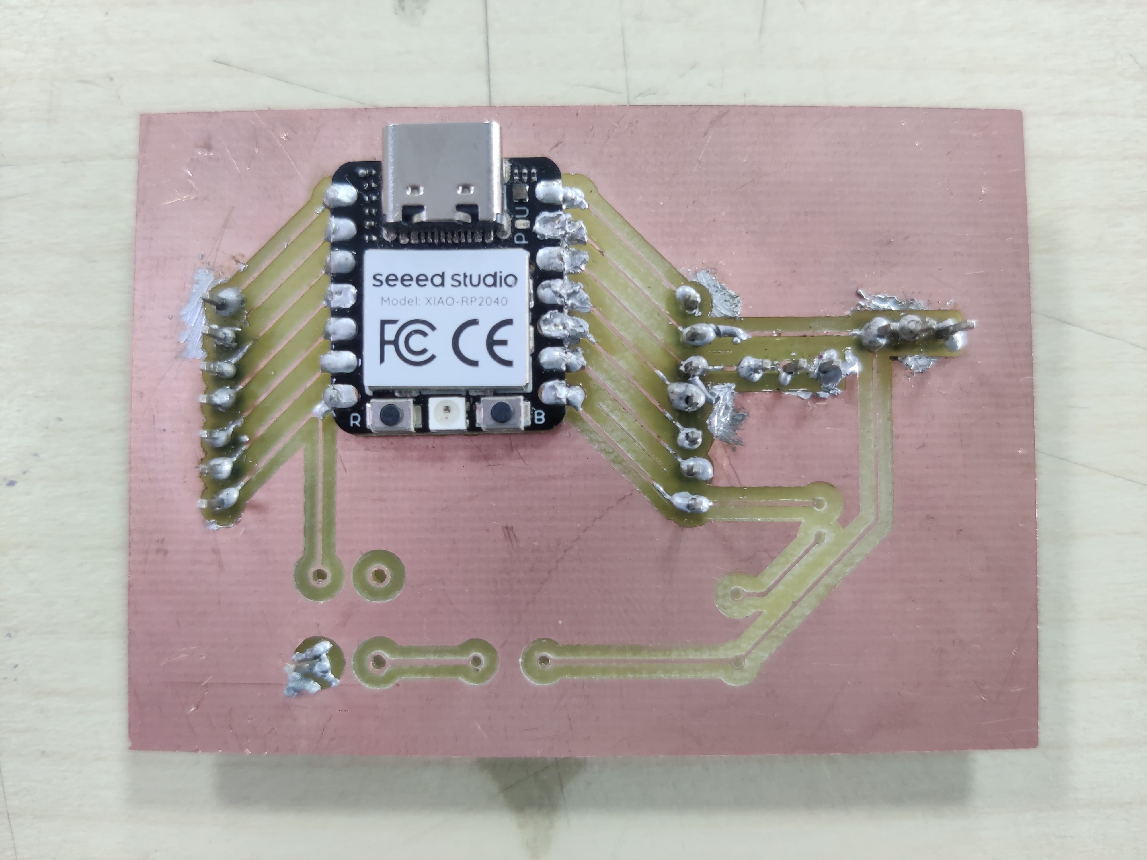
Error while soldering
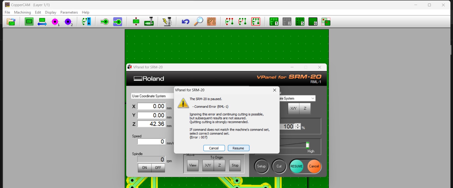
While I was soldering something happened and the RP2040 is not working now, the error needs to be debug yet. SO I made a new PCB and soldered it
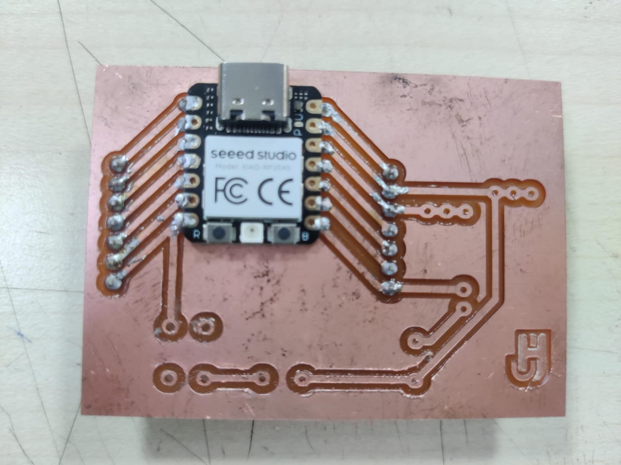
New PCB Milling
Coding
    // Define pin numbers
#define LED_PIN D7
#define BUTTON_PIN D6

// Setup function runs once when you press reset or power the board
void setup() {
  // Initialize LED pin as an output
  pinMode(LED_PIN, OUTPUT);
  // Initialize button pin as an input
  pinMode(BUTTON_PIN, INPUT_PULLUP);
}

// Loop function runs repeatedly as long as the board has power
void loop() {
  // Check if the button is pressed
  if (digitalRead(BUTTON_PIN) == LOW) { // Button is active low
    // Turn on the LED
    digitalWrite(LED_PIN, HIGH);
  } else {
    // Turn off the LED
    digitalWrite(LED_PIN, LOW);
  }
}
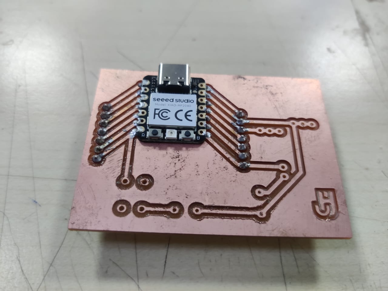
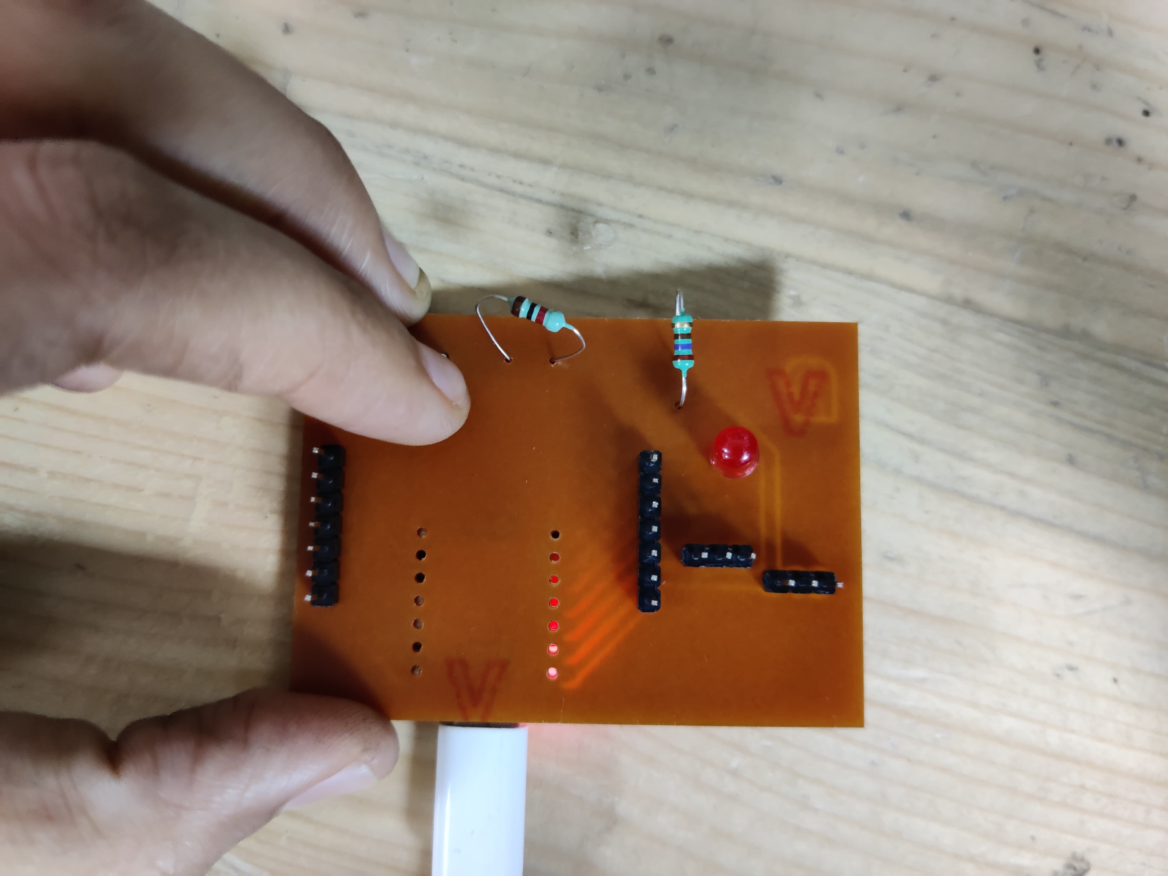
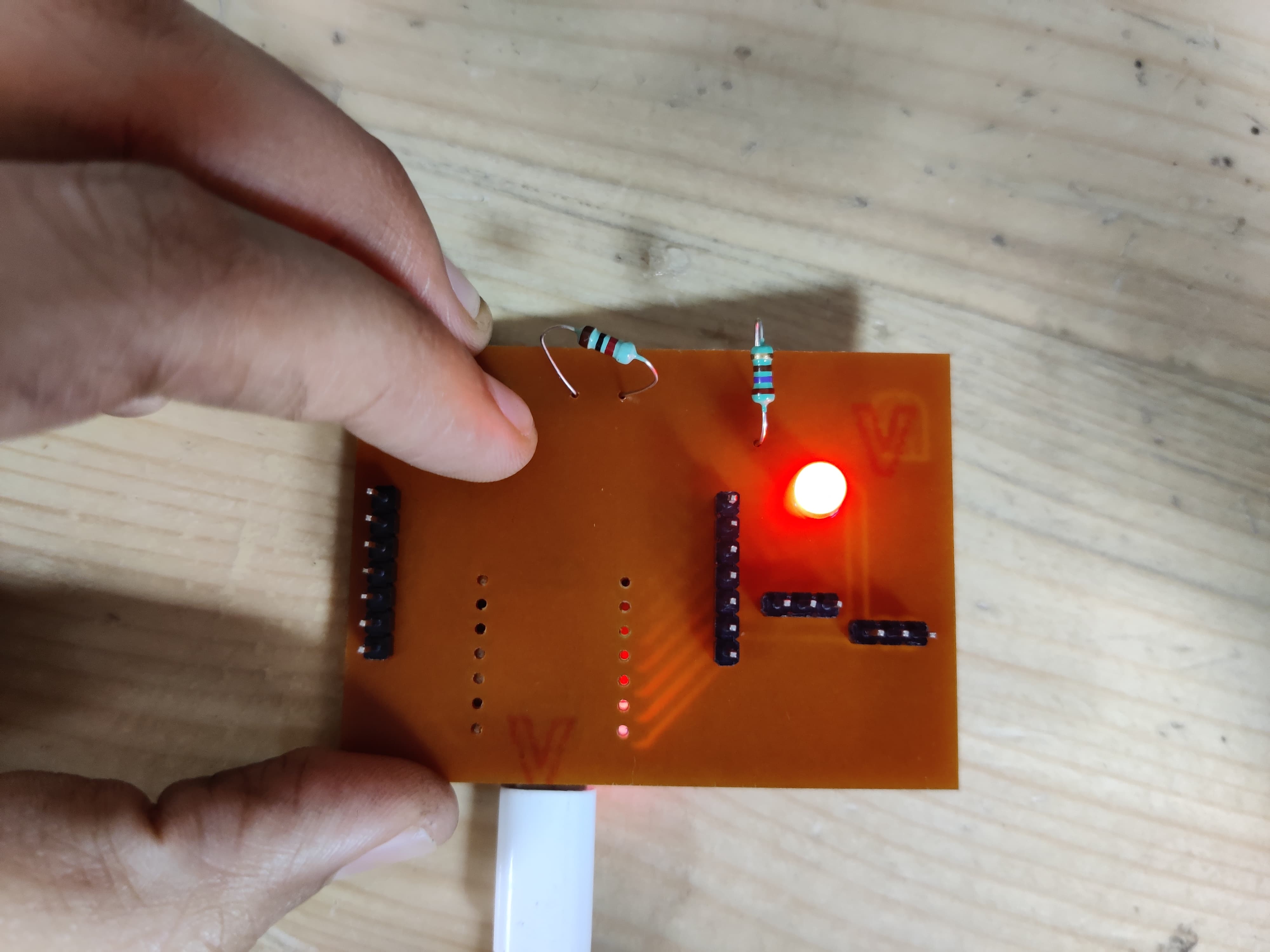
Heroshot of testing the devboard
For testing if I switch on the button on the board then the led should light up was the testing.
Group Work
Task:
Use the test equipment in your lab to observe the operation of a microcontroller circuit board (as a minimum, you should demonstrate the use of a multimeter and oscilloscope)
Document your work on the group work page and reflect what you learned on your individual page
What is Osciloscope
An Oscilloscope is instrument that graphically displays electrical signals.
and shows how voltage changes over time.
The osciloscope which we have is 17 mega hutz frequency and we can record from 1 giga sample per second.
Why Oscilloscope is used?
The main purpose of oscilloscope is to visualize and analyse the waveform of electrical signals.
The most universal tool for viewing electronics signals is oscilloscope . An oscilloscope provides an accurate image of an electronic signal and how that signal changes over time. An accurate waveform lets you take accurate measurement of the signal.
We started with understanding the keys and features of osciloscope first we referred to this link for understanding that Link
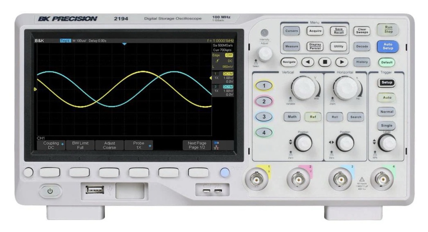
Front Panel
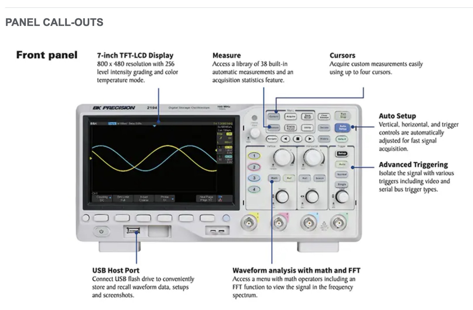
The front panel of the oscilloscope features a 7-inch TFT-LCD display with 800 x 480 resolution, providing clear visual output. It includes advanced triggering options, waveform analysis with math and FFT, and a convenient USB host port for data storage and recall.
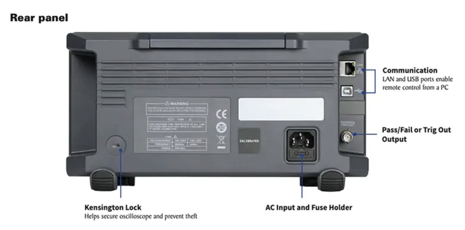
Rear Panel
The rear panel is equipped with LAN and USB ports for remote control from a PC, a pass/fail or trigger out output, and an AC input with a fuse holder. It also includes a Kensington lock for secure usage and theft prevention.
After knowing the basics about front and rear panel we went into more details with exploring all the keys which are there on oscilloscope.
Front Panel Detail
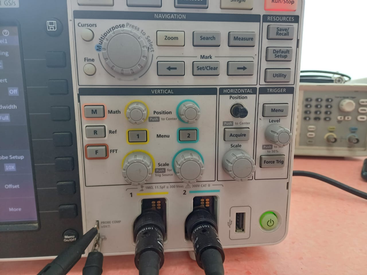
The front panel of the oscilloscope includes various control keys, such as tools, trigger, and horizontal controls, as well as the USB host port and analog channel inputs. The detailed layout allows for precise adjustments and easy access to essential functions.
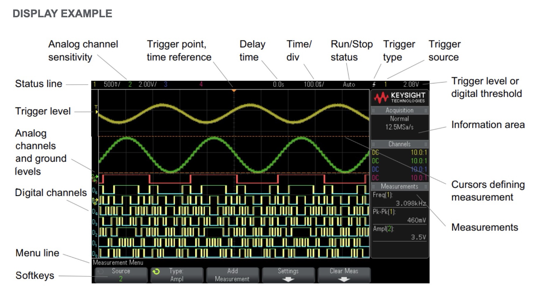
Display Example
The oscilloscope display provides comprehensive information including analog and digital channel sensitivity, trigger point, delay time, and measurement cursors. The clear visual indicators and labeled sections enhance user understanding and analysis of signal data.
Segments
The oscilloscope has 3 segments vertical, horizontal and triger controls.
How to use Oscilloscope.
Step 1: Power On the Oscilloscope
Plug In: Connect the oscilloscope to a power source.
Power On: Press the power switch to turn on the oscilloscope.
Step 2: Connect the Probes
Probe Connection: Connect the oscilloscope probes to the input channels (analog channel inputs).
Ground Clip: Attach the probe’s ground clip to a ground point on your circuit to ensure accurate measurements.
Step 3: Configure the Oscilloscope
1. Auto Setup: Press the [Auto Setup] key to automatically adjust vertical, horizontal, and trigger settings for an optimal display.
2. Manual Adjustments:
a. Vertical Controls: Use the vertical controls to set the volts/div (voltage per division) to scale the signal appropriately.
b. Horizontal Controls: Adjust the time/div (time per division) to set the time base for the signal.
Step 4: Trigger Settings
Trigger Type: Select the appropriate trigger type (edge, pulse, etc.) using the trigger controls.
Trigger Level: Adjust the trigger level to stabilize the waveform display.
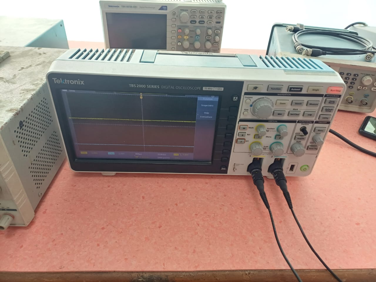
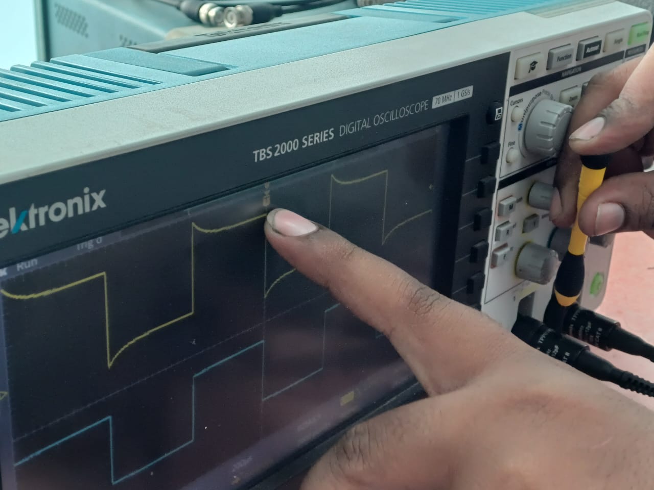
We did the calibration manually here, in vertical we have 2 options one is channel 1 which is yellow in colour and the other one is channel 2 which is blue in colour , so we connected channel 1 first.
There is an option of posistioning waves so if you click once on chanel 1 the waves come in center and if you double click chnael 1 it will get off so if you don't need any one of them channel then off it.
Now the waves which you can see should be square waves and it should not move continuous so we need to stop the wave.Use trigger function for that then it will be perfectly rectangle. But in case sometimes it is over powered and lowered powered then take a screw driver and put it in the holes, then it will be completely allign, so there are 2 place to put screw one is over and one is lower, so with the help of screw driver if there is any marginal error correct it with that.
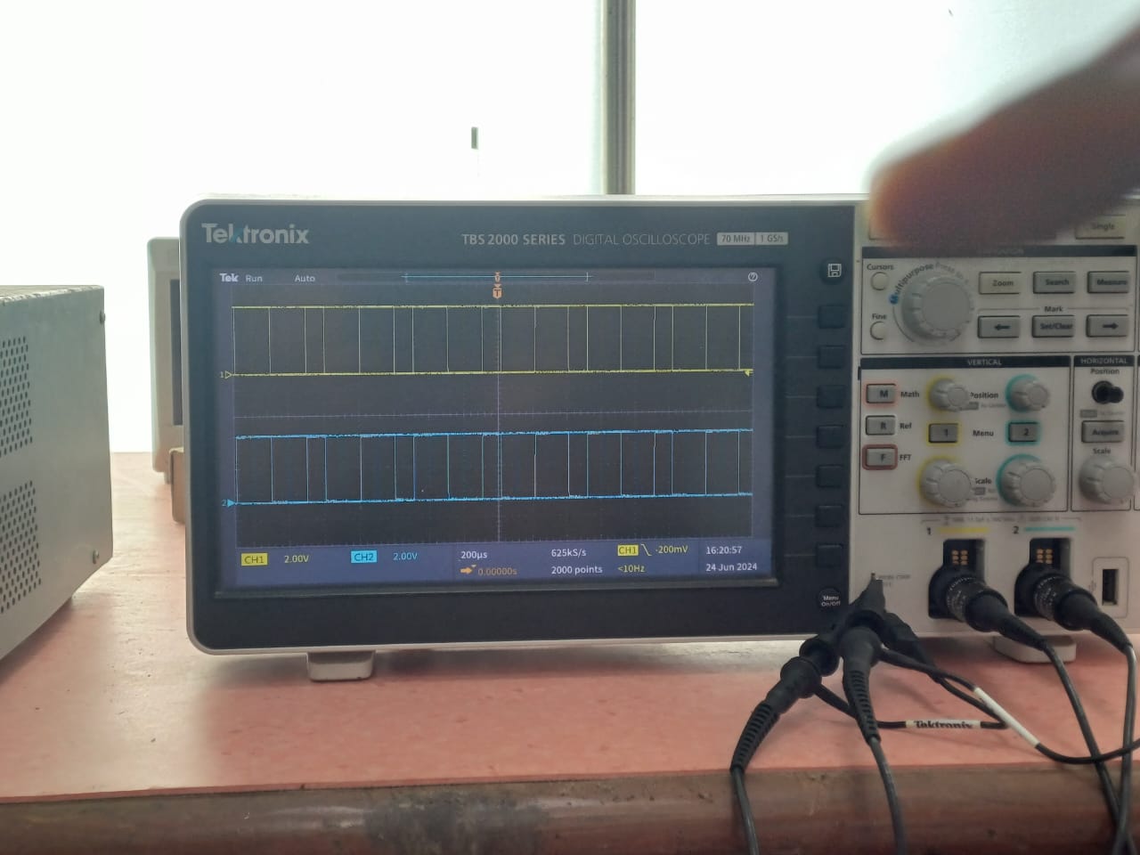
Step 5: Acquire and View Signals
Run Control Keys: Use the run/stop button to start and stop signal acquisition.
Display Analysis: Analyze the signal on the display. Use the cursors to measure specific points on the waveform and the measure controls to access built-in measurement features.
Suggestion
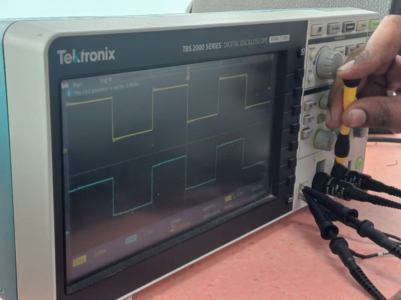
In channel 1 we have some settings, so the first settings is coupling, we use couplings to test signal so if you only need dc signals while testing your circuit then select dc if you select ac then ac will completely boycott your dc signals and you can't analyse it. If you keep it on dc then dc will allow you to analyse ac as well.
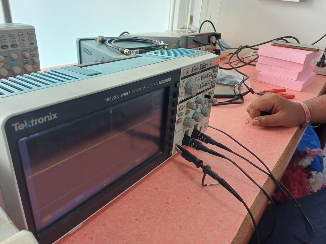
We connected both probes on led and tested the signals.
We did not use this step, it depends on what are you measuring.
Step 6: Save and Document Data
USB Host Port: Insert a USB drive into the USB host port to save waveform data, screenshots, and setup configurations.
File Keys: Use the file keys to navigate and save your data to the USB drive.
Step 8: Safety and Maintenance
Turn Off: Power off the oscilloscope when not in use.
Disconnect Probes: Safely disconnect the probes from the circuit and oscilloscope.
Store Properly: Store the oscilloscope and probes in a safe, dry place to prevent damage.
Hero Shot
Conclusion from this week
During Electronic Design Week, we focused on both group and individual assignments that deepened our understanding of microcontroller circuit boards and PCB design. As a group, we used lab test equipment to observe the operation of a microcontroller circuit board and successfully sent a PCB design to a board house, JLCPCB. Individually, I used EasyEDA to design, produce, and test a development board for interacting with an embedded microcontroller. This week provided valuable hands-on experience with electronic design automation tools and the practical aspects of PCB production, enhancing my skills in designing and testing electronic circuits.
Design Files
Image Credits
All images of cover page are credited below:
https://images.app.goo.gl/Ztt9R31eHpH57b9t8
https://images.app.goo.gl/jzDY3RbNeC4RTcAx9