Electronics Production
Electronic Production seems daunting to me. I've always felt uneasy about anything related to electronics engineering, especially since my background is in commerce and I have little connection to science. Despite having some exposure to Arduino in the past, I've forgotten most of it and had to start over from the beginning. This week's assignment involved understanding the design rules for our in-house PCB production process, sending a PCB to a board house, and creating and testing a microcontroller development board.
Basic concepts of Electronics
Electricity:
Electricity is the flow of electric charge. It can be generated by sources such as batteries, generators, and solar cells.
Voltage:
Voltage, also known as electric potential difference, is the force that drives electric charge through a circuit. It is measured in volts (V) and represents the energy per unit charge.
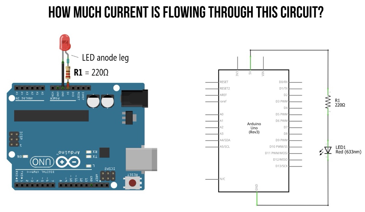
Current:
Electric current is the flow of electric charge through a conductor. It is measured in amperes (A). Current flows from higher voltage to lower voltage, driven by the voltage difference.
Resistance:
Resistance is the opposition to the flow of electric current. It is measured in ohms (Ω). Materials with high resistance impede the flow of current, while those with low resistance allow current to flow easily.
Ohm's Law:
Ohm's Law states that the current through a conductor between two points is directly proportional to the voltage across the two points, and inversely proportional to the resistance between them. It can be expressed as V = I * R, where V is voltage, I is current, and R is resistance.
Circuit:
A circuit is a closed path through which electric current can flow. It typically consists of a power source (such as a battery), conductors (wires), and loads (such as resistors, capacitors, and inductors).
Series Circuit:
In a series circuit, components are connected end-to-end, so the same current flows through each component. The total resistance in a series circuit is the sum of the individual resistances.
Parallel Circuit:
In a parallel circuit, components are connected across common points, so the voltage across each component is the same. The total resistance in a parallel circuit is less than the smallest individual resistance.
Capacitance:
Capacitance is the ability of a component, called a capacitor, to store electrical energy in an electric field. It is measured in farads (F).
Inductance:
is the property of a component, called an inductor, to store energy in a magnetic field when current flows through it. It is measured in henrys (H).
Types of circuits
There are primarily two types of circuit configurations: series circuits and parallel circuits. Let's delve into each type:
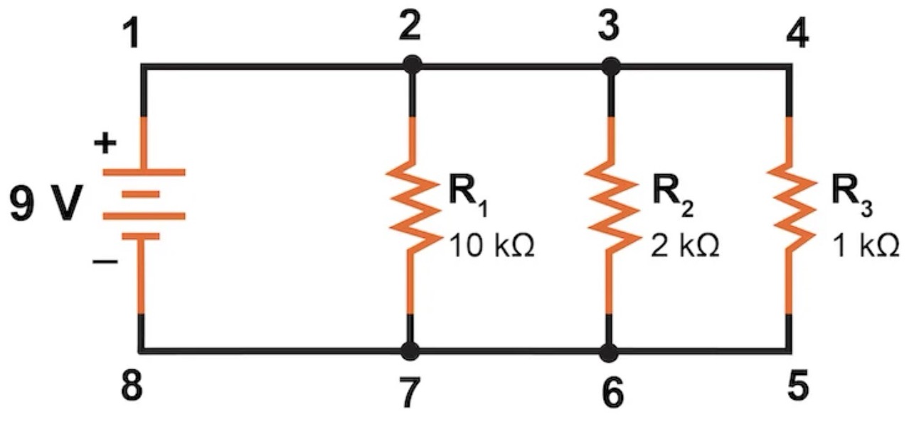
1. Series circuit
In a series circuit, components are connected end-to-end in a single path so that the same current flows through each component. It forms a loop with no branches.
Characteristics:
a. The total resistance in a series circuit is the sum of the individual resistances.
b. The total voltage across the circuit is the sum of the voltages across each component.
c. If one component in a series circuit fails or is removed, the entire circuit becomes open and current stops flowing.
Example:
Consider three resistors (R1, R2, R3) connected in series to a battery. The total resistance (RT) would be RT = R1 + R2 + R3.
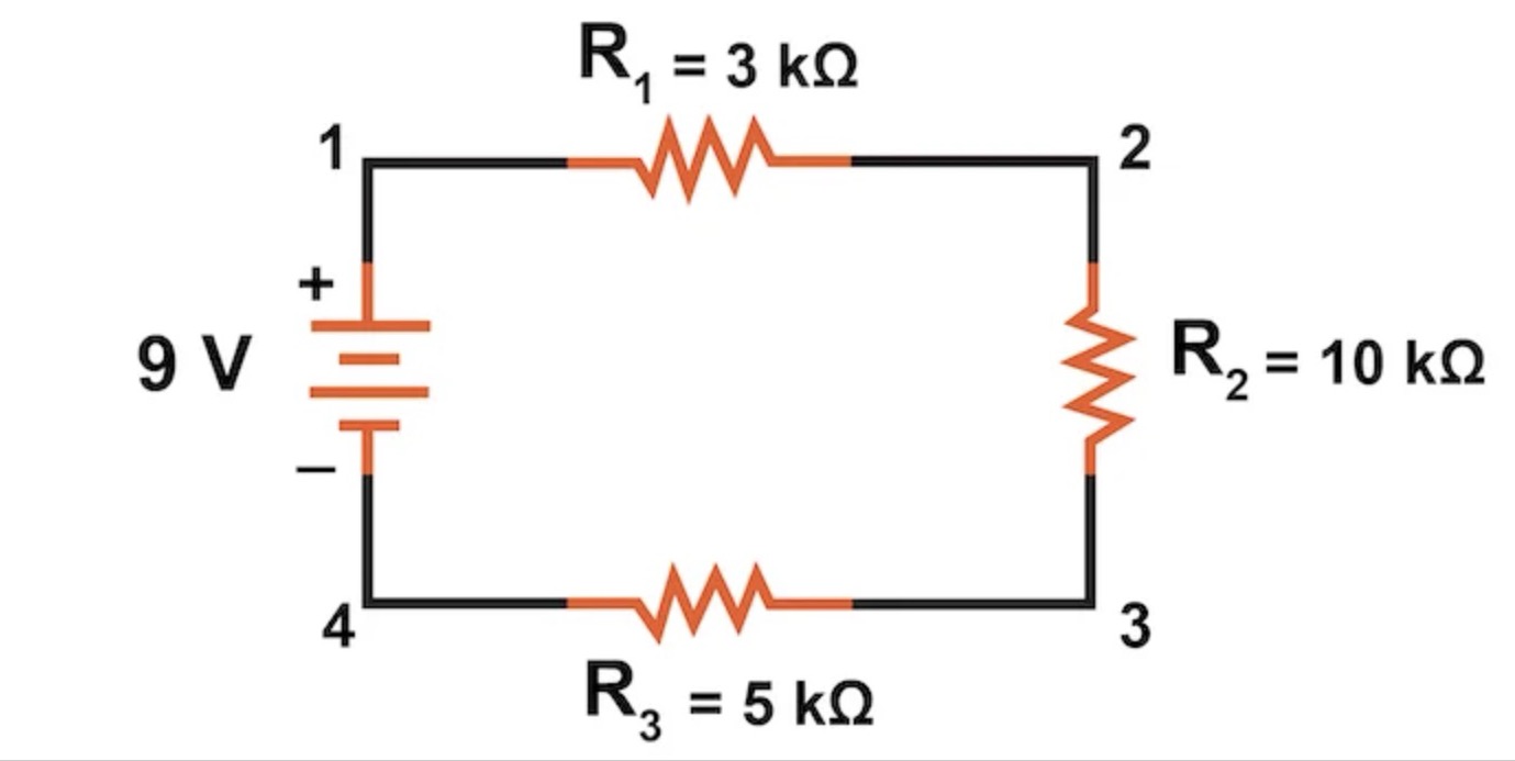
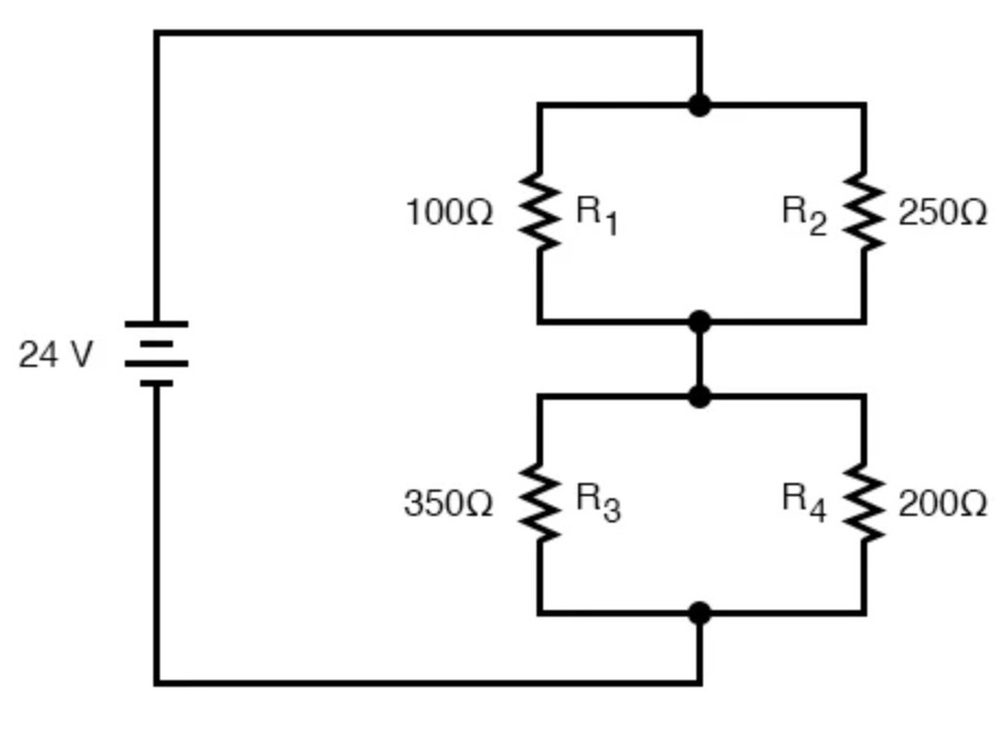
2. Parallel Circuit:
In a parallel circuit, components are connected across common points, forming multiple paths for current flow. Each component has the same voltage across it.
Characteristics:
a. The total resistance in a parallel circuit is less than the smallest individual resistance.
b. The total current in a parallel circuit is the sum of the currents through each branch.
c. If one component in a parallel circuit fails, the current can still flow through other branches.
Example:
Consider three resistors (R1, R2, R3) connected in parallel to a battery. The reciprocal of the total resistance (1/RT) would be 1/RT = 1/R1 + 1/R2 + 1/R3.
Series-Parallel Circuits:
Series-parallel circuits are combinations of series and parallel circuits. Components can be connected in both series and parallel configurations within the same circuit.
Characteristics:
a. They offer flexibility in designing circuits with various functionalities.
b. Analysis can be more complex compared to purely series or parallel circuits.
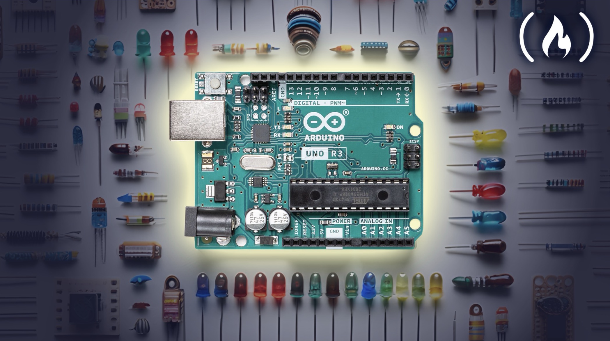
What is Arduino
Arduino is an open-source electronics platform based on easy-to-use hardware and software. It consists of a microcontroller and a development environment that allows for the creation of interactive electronic projects. Arduino boards are equipped with input and output pins that can be programmed to interact with sensors, actuators, and other electronic components. They are widely used by hobbyists, students, artists, and professionals to prototype and build a variety of electronic systems, ranging from simple blinking LED projects to complex robotics and IoT applications.
Imput and Output devices
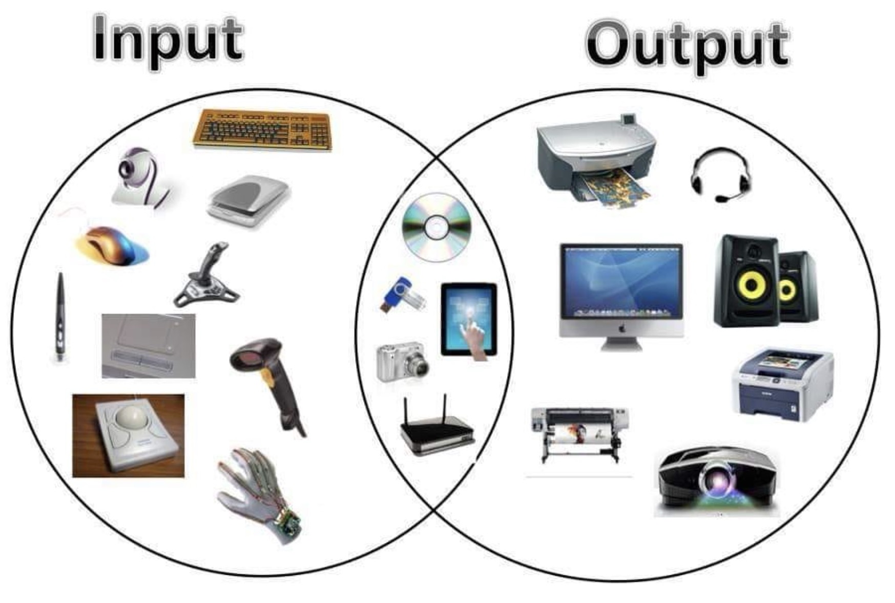
3. Imput devices
Input devices are components that allow users to interact with electronic systems by providing input signals. They capture data from the environment or user input and send it to the system for processing.
Examples:
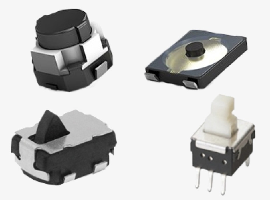
a. Switches:
Mechanical or electronic devices used to open or close a circuit, such as push buttons, toggle switches, and pressure sensors.
b. Sensors:
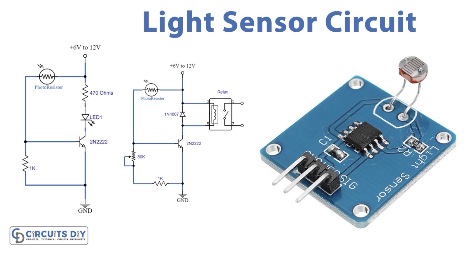
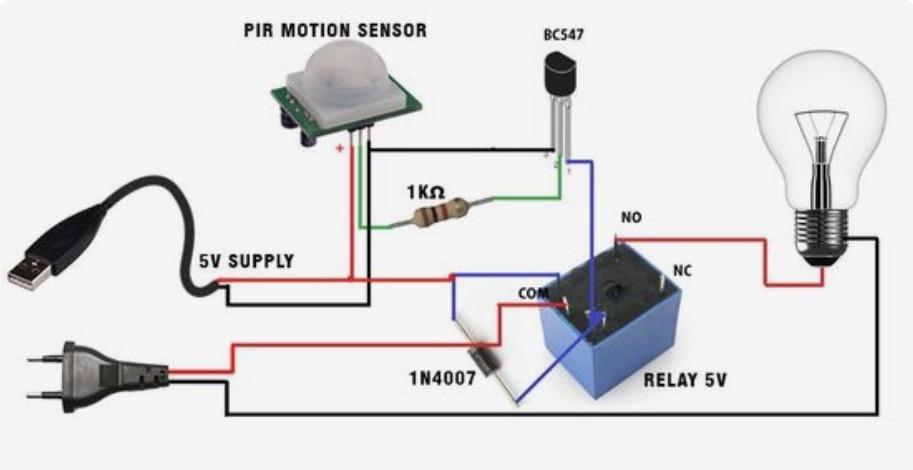
Devices that detect changes in the environment and convert them into electrical signals, including temperature sensors, light sensors, motion sensors, and gas sensors.
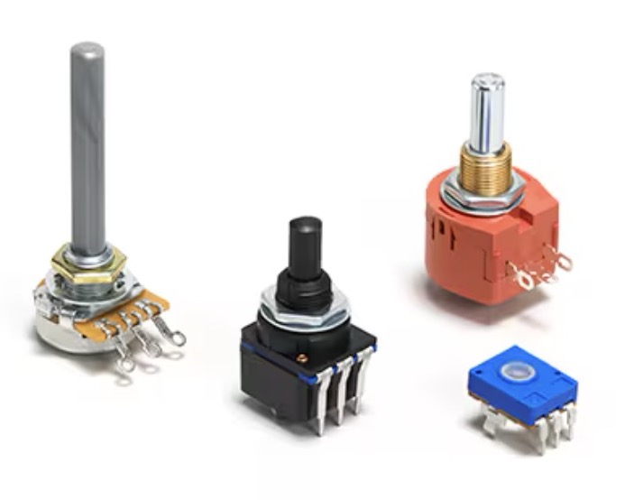
c. Potentiometers:
Variable resistors used to adjust the voltage or resistance in a circuit, commonly used for volume control, dimmer switches, and analog input. Keyboards and Keypads: Input devices for entering alphanumeric characters and commands into electronic systems.
2. Output devices
Output devices are components that display information or respond to signals generated by electronic systems. They provide feedback to users or control external processes based on the system's output.
Examples:
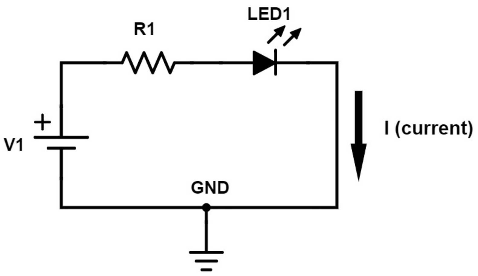
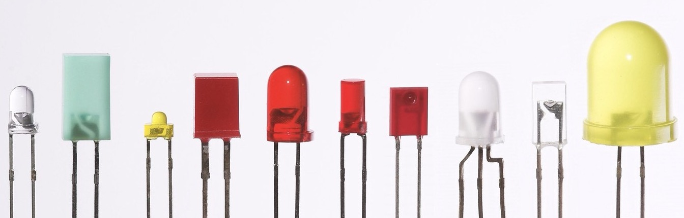
a. LEDs (Light-Emitting Diodes):
Semiconductor light sources that emit light when current flows through them, used for visual indicators, displays, and illumination.
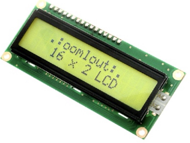
b. LCD (Liquid Crystal Display) and LED Displays:
Display modules that present text, numbers, or graphics to users in electronic devices, such as digital watches, calculators, and meters.
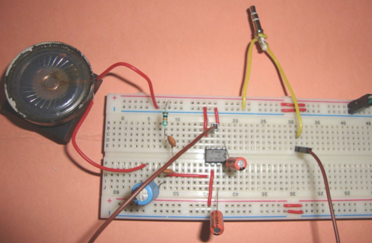
c. Speakers:
Transducers that convert electrical signals into audible sound waves, used for audio output in devices such as smartphones, computers, and alarm systems.
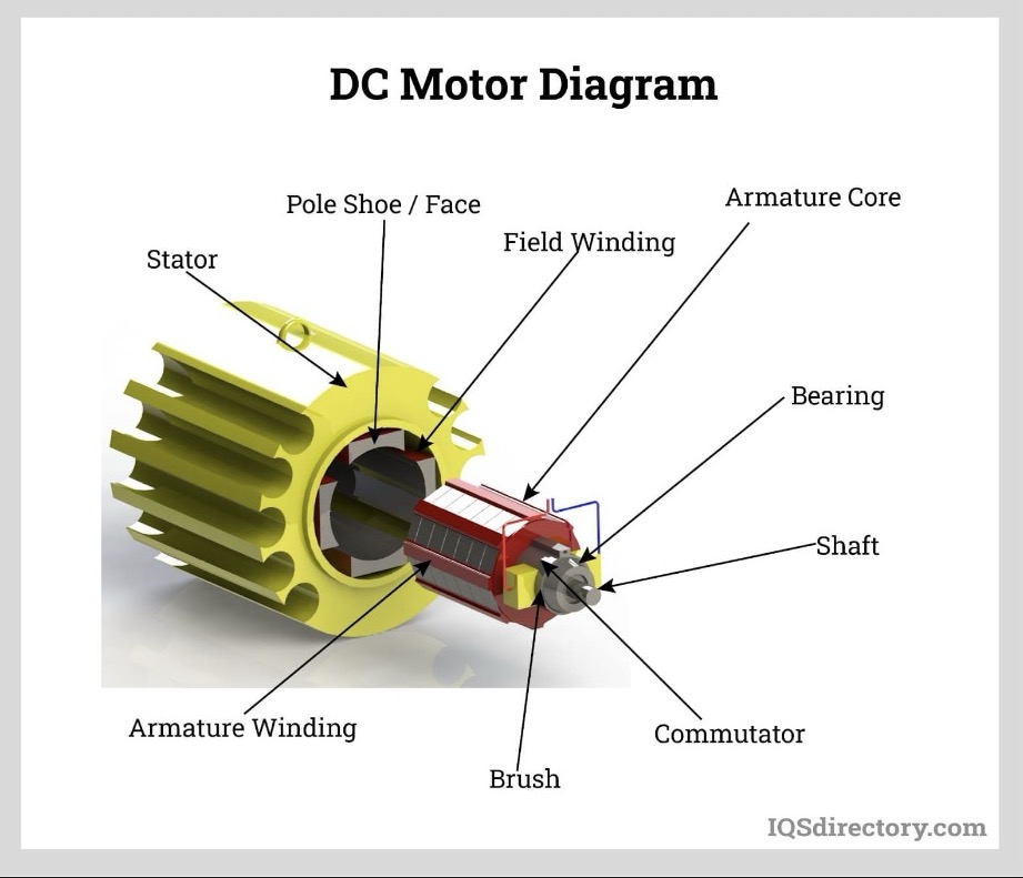
d. Motors:
Devices that convert electrical energy into mechanical motion, including DC motors, stepper motors, and servo motors, used in robotics, automation, and electromechanical systems.
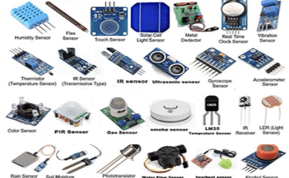
Sensors
Sensors are electronic devices or modules that detect changes in physical or environmental conditions and convert them into electrical signals. These signals can be processed by electronic systems to monitor, control, or respond to the detected changes. Sensors are widely used in various applications, including industrial automation, environmental monitoring, healthcare, and consumer electronics. Some common types of sensors include:
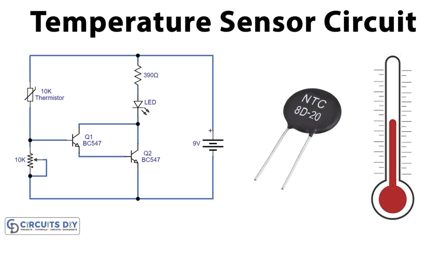
a. Temperature Sensors:
Measure temperature changes in the environment or objects.
b. Light Sensors:
Detect light intensity or ambient brightness levels.
c. Motion Sensors:
Detect movement or changes in position.
d. Pressure Sensors:
Measure changes in pressure or force.
e. Humidity Sensors:
Measure relative humidity or moisture levels in the air.
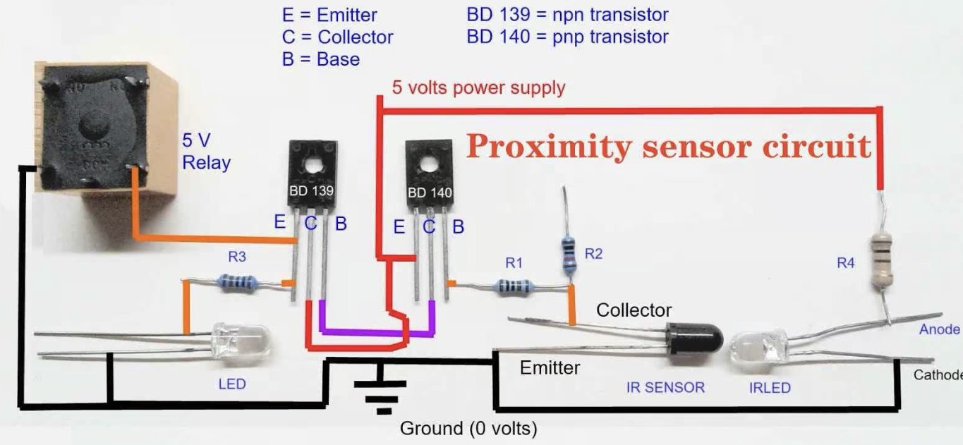
f. Proximity Sensors:
Detect the presence or absence of nearby objects without physical contact.
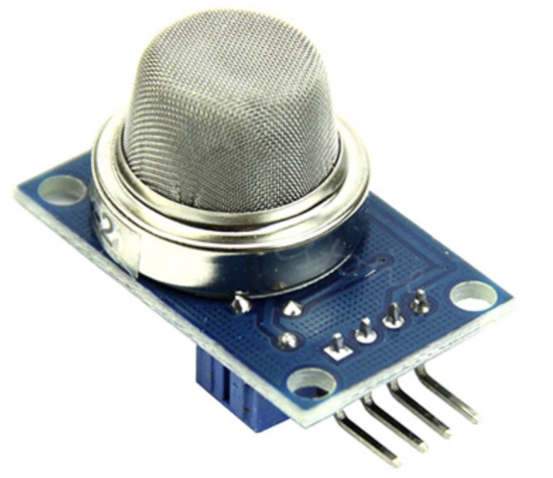
g. Gas Sensors:
Detect the presence and concentration of gases in the environment.
h. Biometric Sensors:
Measure biological data, such as heart rate, fingerprints, or retinal patterns, for authentication or health monitoring purposes.
Sensors play a crucial role in gathering data from the physical world and enabling electronic systems to interact with and adapt to their surroundings effectively. They are essential components in a wide range of electronic devices and systems, enabling capabilities such as environmental monitoring, automation, and human-machine interaction.
Components on arduino board
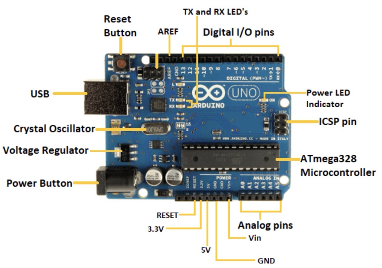
1. Microcontroller:
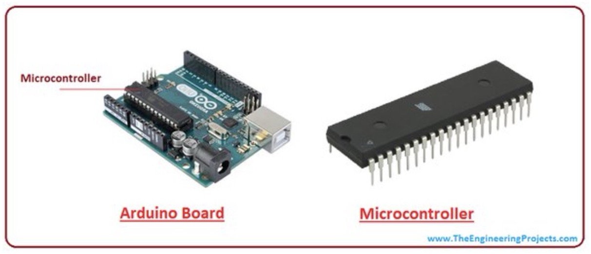
The heart of the Arduino board is a microcontroller, which is a small integrated circuit (IC) that contains the processor (CPU), memory (RAM and ROM), and various peripherals necessary for controlling electronic devices. The most commonly used microcontroller in Arduino boards is the Atmel AVR series, such as the ATmega328P or ATmega2560. However, some newer Arduino boards also use other microcontrollers, such as the ARM Cortex-M series.
2. Input/Output (I/O) Pins:
Arduino boards feature a set of digital and analog input/output pins that allow the microcontroller to communicate with external devices, such as sensors, actuators, and other electronic components. These pins can be configured as either inputs or outputs and can be used for tasks such as reading sensor data, controlling LEDs, driving motors, and communicating with other devices via protocols like SPI, I2C, and UART.
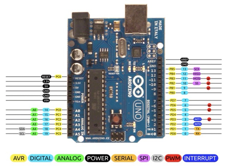
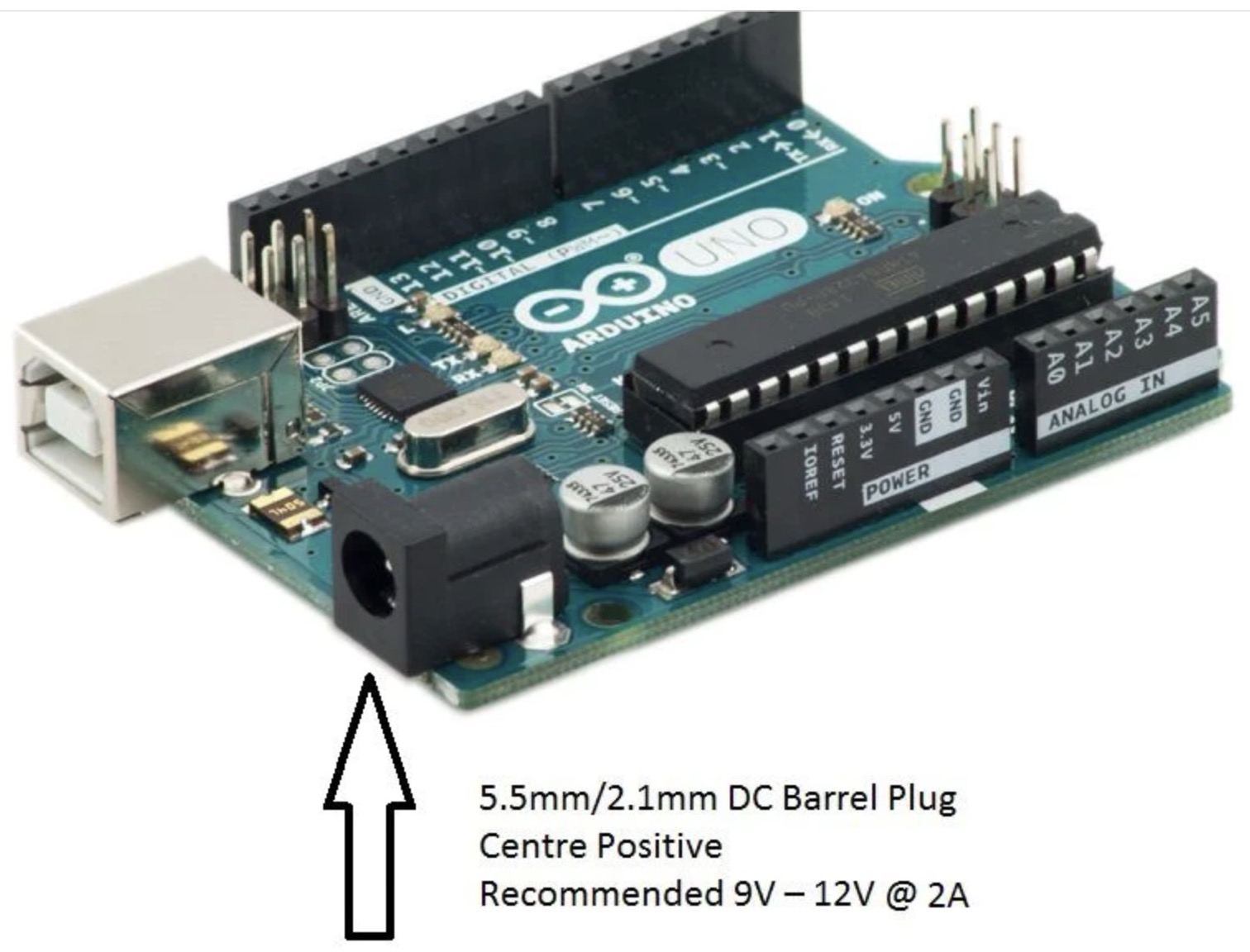
3. Power Supply:
Arduino boards can be powered in various ways, including via USB connection, external power supply, or battery. They typically include voltage regulators to provide stable voltage levels for the microcontroller and other components. Some Arduino boards also feature additional power-related components, such as power jacks or battery connectors.
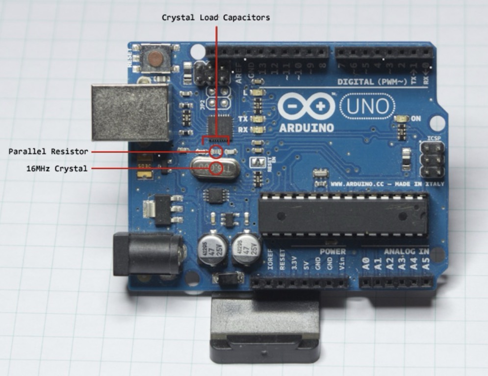
4. Clock Crystal/Resonator
To keep track of time and synchronize operations, Arduino boards often include a clock crystal or resonator, which generates precise clock signals for the microcontroller.
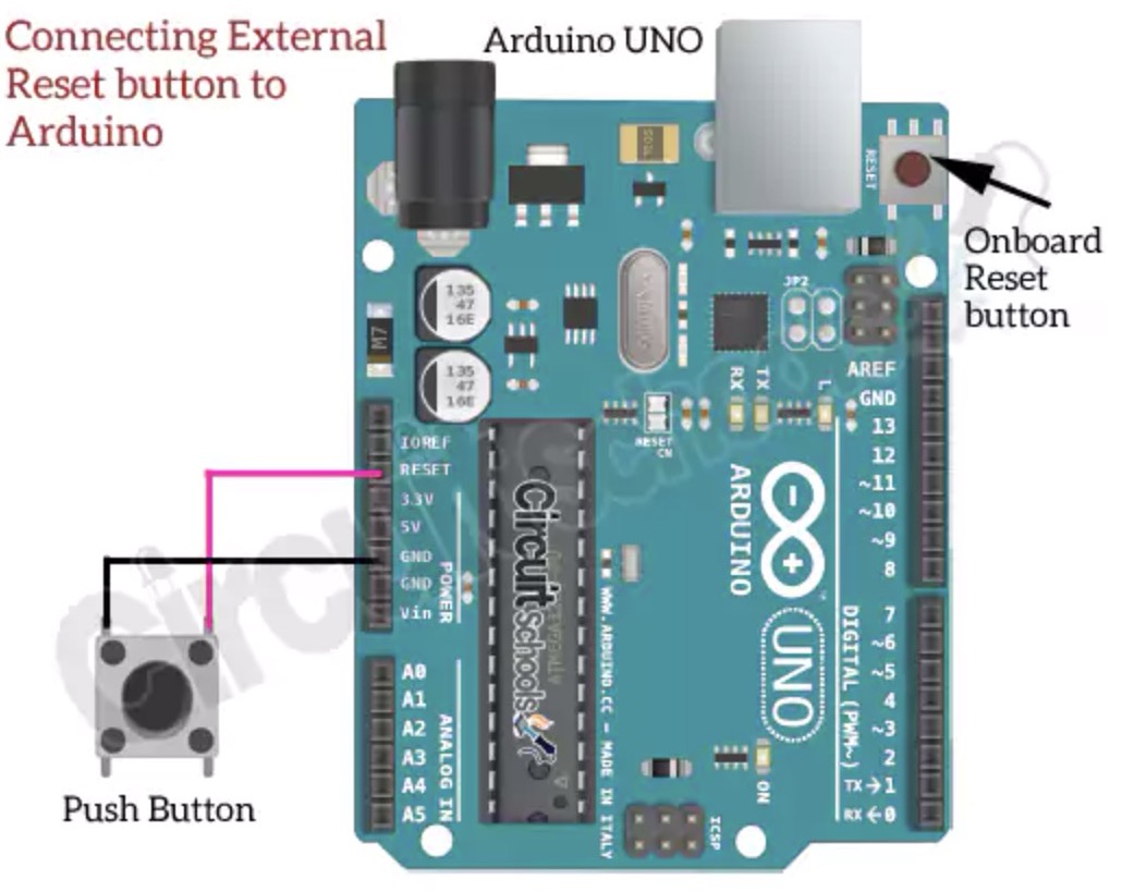
5. Reset Button:
A reset button allows you to restart the Arduino board, resetting the microcontroller and restarting the code execution from the beginning.
6. LEDs:
Many Arduino boards include built-in LEDs that can be used for visual feedback or debugging purposes. These LEDs are often connected to specific pins on the microcontroller and can be controlled via software to indicate various states, such as power status, communication activity, or program execution.
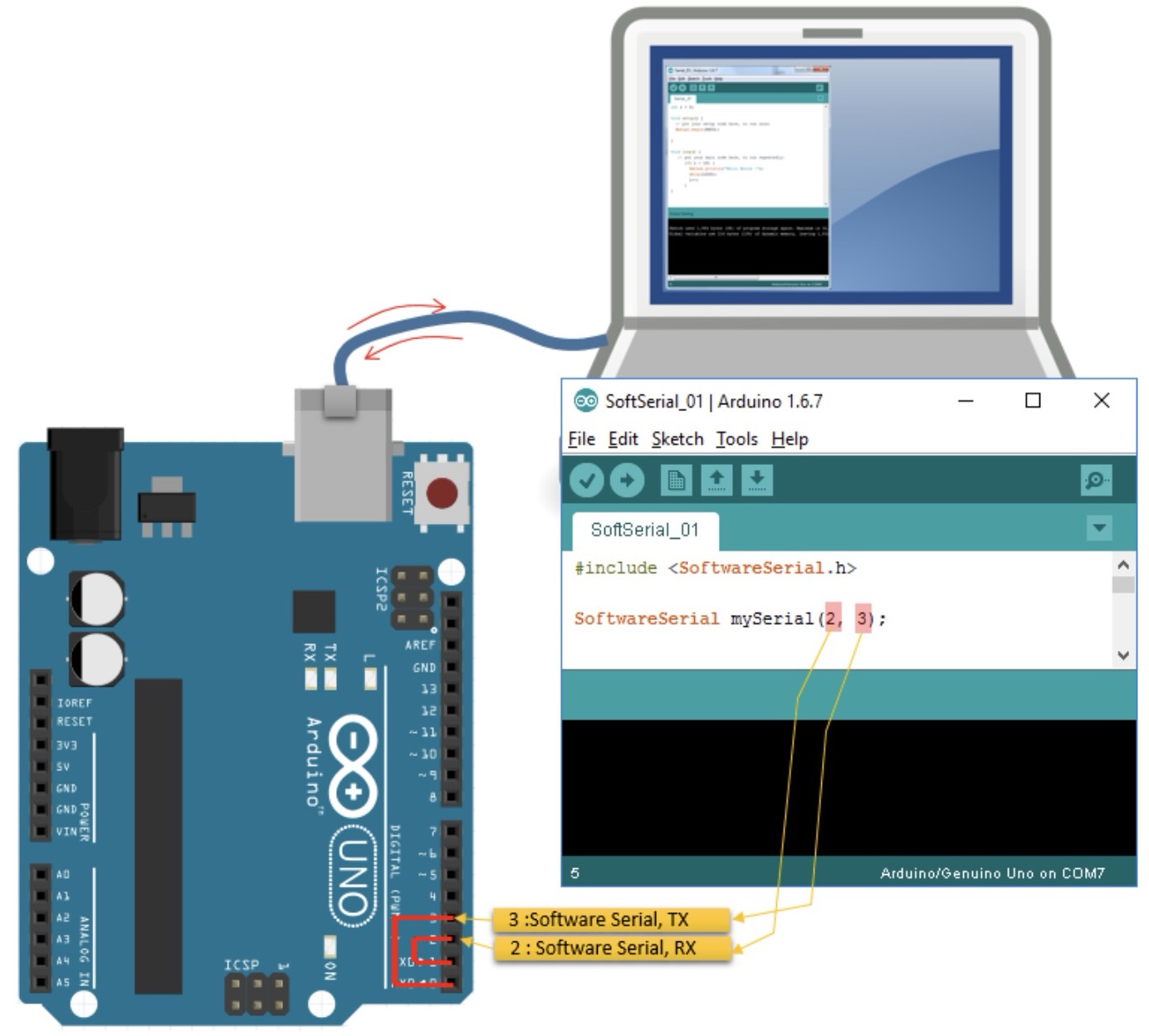
7. Serial Interface:
Arduino boards typically include a USB-to-serial interface chip that allows them to communicate with a computer via USB. This interface is used for programming the Arduino board and for serial communication with the microcontroller during development and debugging.
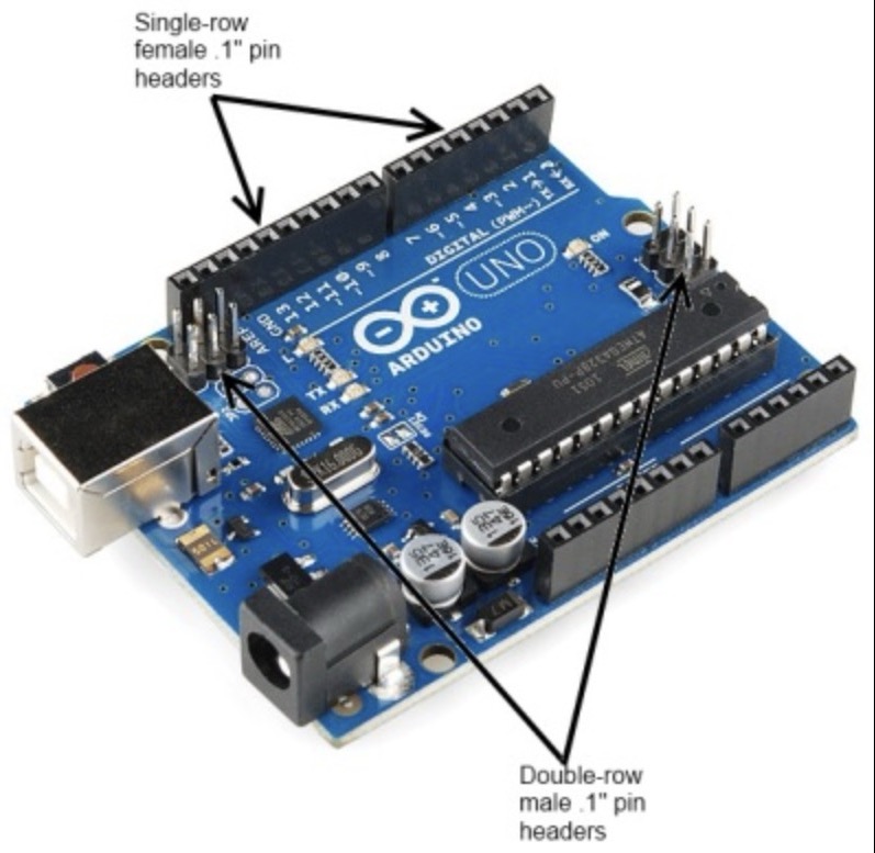
8. Headers and Connectors:
Arduino boards feature various headers and connectors that provide access to the input/output pins, power supply, and other interfaces. These headers allow you to connect external devices, modules, and shields to expand the capabilities of the Arduino board.
To see everything together, check the image below
What is a PCB?
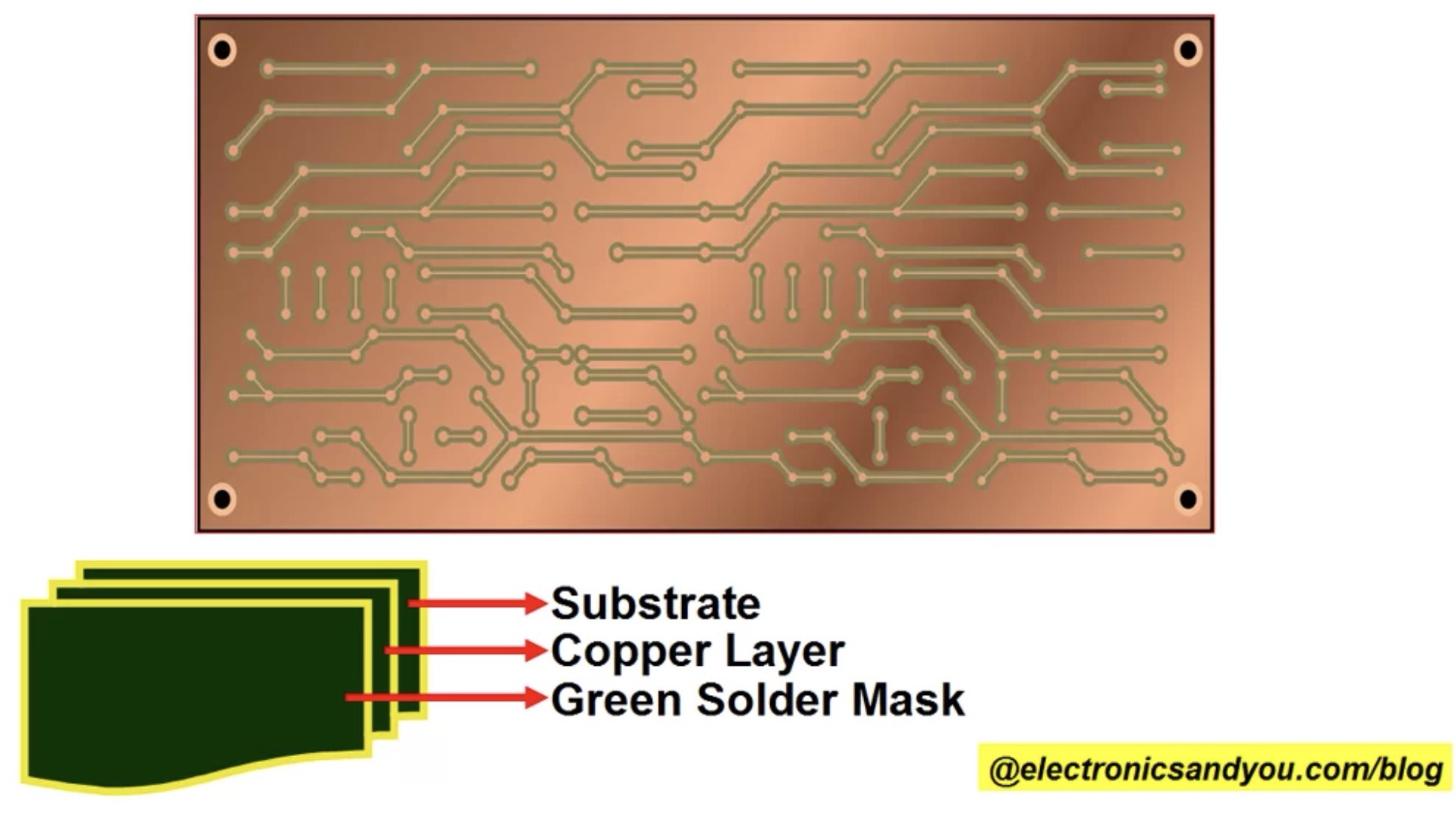
A PCB, or Printed Circuit Board, is a flat board made of non-conductive material, usually fiberglass-reinforced epoxy resin (FR-4), onto which electronic components are mounted and interconnected. It serves as the structural and electrical foundation for electronic circuits, providing mechanical support for components while facilitating reliable electrical connections between them. Conductive traces, typically made of copper, are etched or printed onto the surface of the PCB to create pathways for electrical signals to flow between components. Components are mounted onto the PCB using soldering techniques, either through holes drilled in the board for through-hole components or directly onto the surface for surface-mount components. PCBs also feature solder mask and silkscreen layers for insulation, protection, and component identification. Vias are used to connect conductive traces between different layers of the PCB in multi-layer designs. PCBs are fundamental elements in virtually all electronic devices and systems, enabling compact and reliable circuit construction for a wide range of applications.
Types of PCB'S
1. Single-Layer PCBs
Single-layer PCBs have conductive traces and components on only one side of the board. They are often used in simpler electronic devices with fewer components and lower complexity, such as calculators, toys, and LED displays.
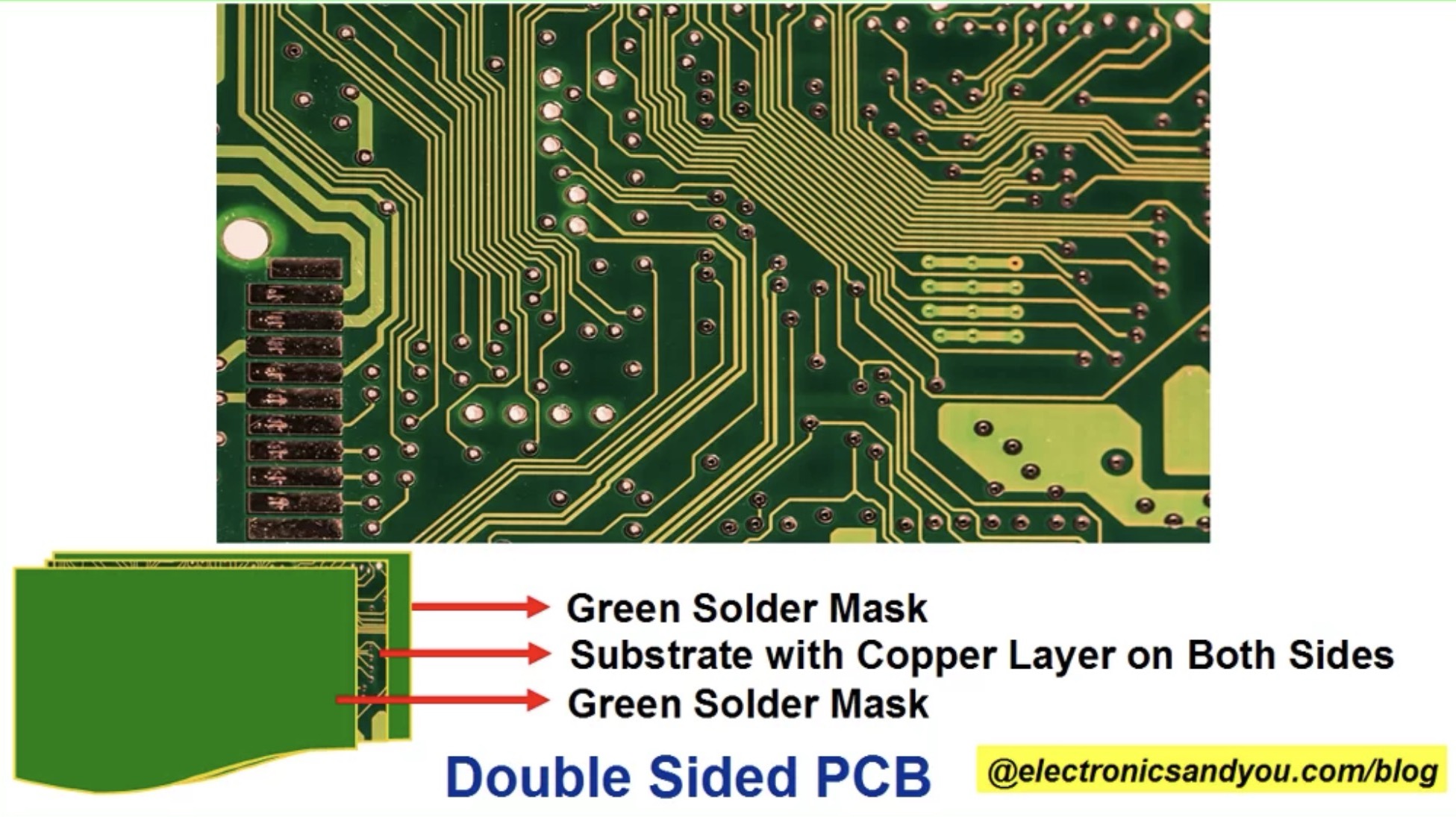
2. Double-Layer PCBs:
Double-layer PCBs have conductive traces and components on both sides of the board. The traces on each side are typically connected through plated-through holes called vias. Double-layer PCBs are used in a wide range of applications, including consumer electronics, industrial controls, and automotive systems.
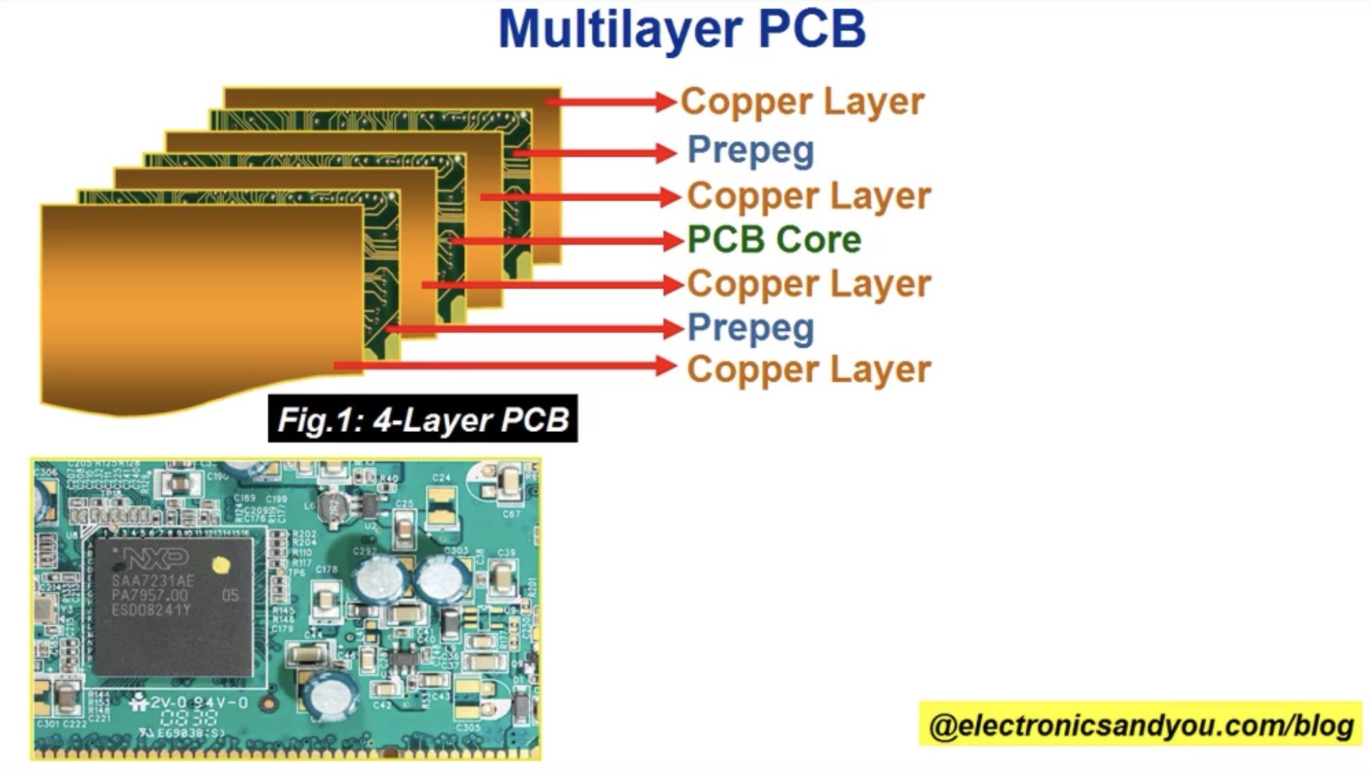
3. Multi-Layer PCBs:
Multi-layer PCBs have three or more layers of conductive traces separated by insulating layers (substrates). These boards can accommodate a large number of components and complex circuits, making them suitable for high-density electronic devices like smartphones, computers, and communication equipment.
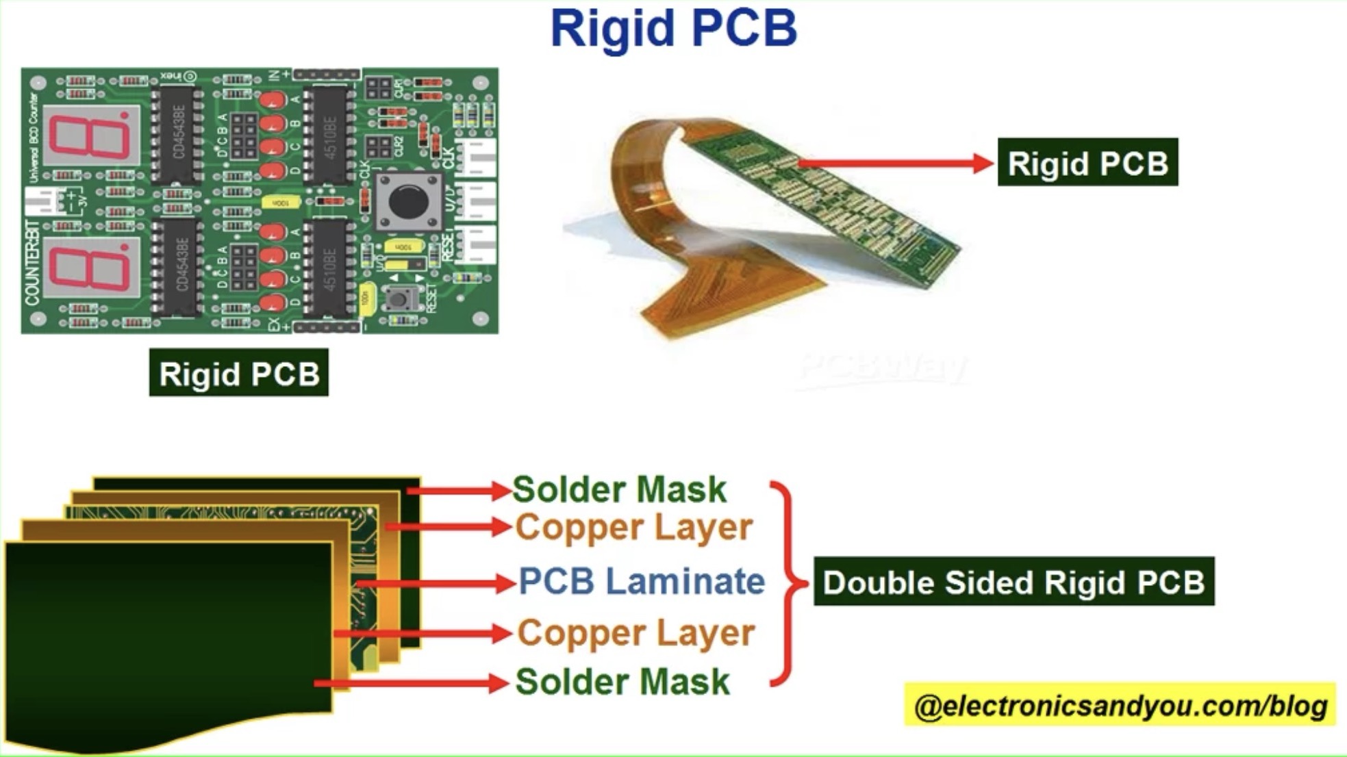
4. Rigid PCBs:
Rigid PCBs are made of solid, inflexible materials such as fiberglass or epoxy resin. They provide excellent mechanical stability and are widely used in most electronic devices and systems.
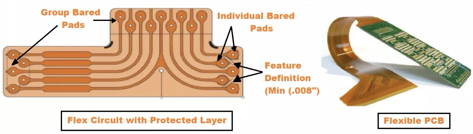
5. Flexible PCBs (FPCBs):
Flexible PCBs are made of flexible materials like polyimide or polyester. They can bend or twist without breaking, making them ideal for applications where space is limited or where the PCB needs to conform to a specific shape, such as in wearable devices, medical devices, and automotive electronics.
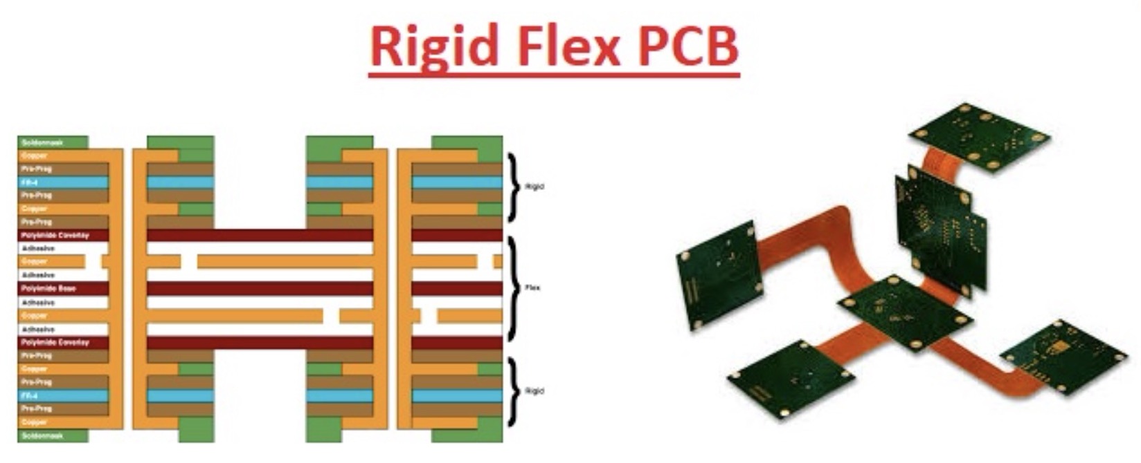
6. Rigid-Flex PCBs:
Rigid-flex PCBs combine elements of both rigid and flexible PCBs, allowing for a combination of rigid and flexible sections within the same board. They offer design flexibility and are commonly used in devices with complex form factors or demanding mechanical requirements, such as foldable smartphones, cameras, and aerospace systems.
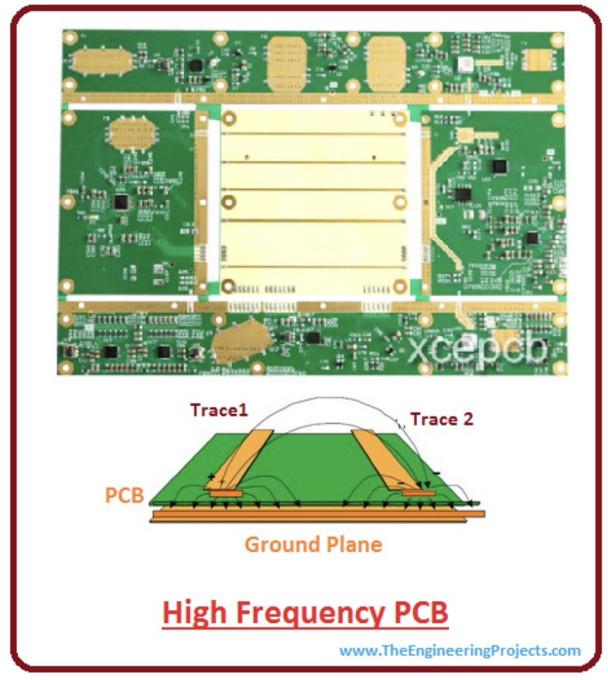
7. High-Frequency PCBs
High-frequency PCBs are designed to handle signals at frequencies above 1 GHz, typically used in RF (radio frequency) and microwave applications. They feature specialized materials and construction techniques to minimize signal loss and impedance mismatch, making them suitable for applications like wireless communication, radar systems, and satellite communication.
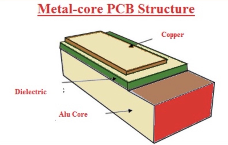
8. Metal Core PCBs (MCPCBs):
Metal core PCBs have a layer of thermally conductive metal, such as aluminum or copper, as the base material instead of fiberglass. They provide efficient heat dissipation and are commonly used in high-power LED lighting, power converters, and automotive electronics.
PCB Production Process
PCB production techniques involve several processes that transform raw materials into finished printed circuit boards (PCBs). Here's an overview of the typical PCB production process:
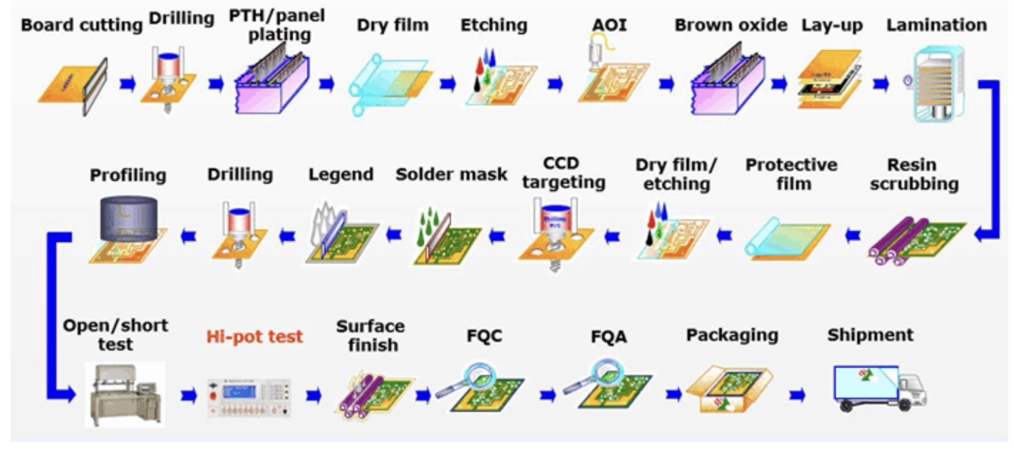
1. Design and Layout:
PCB production begins with the design and layout of the circuit board. This involves using specialized software to create a schematic diagram of the circuit and then designing the physical layout of the PCB, including the placement of components and routing of traces.
2. Substrate Preparation:
a. Substrate Material Selection:
The choice of substrate material, such as FR-4 (fiberglass-reinforced epoxy), polyimide, or metal core, depends on factors like mechanical strength, thermal properties, and cost.
b. ubstrate Cutting:
The substrate material is cut into the desired size and shape using CNC (Computer Numerical Control) machines or cutting tools.
3. Copper Cladding:
a. Cleaning and Surface Preparation:
The substrate surface is cleaned and treated to remove any contaminants and promote adhesion.
b. Copper Deposition:
A thin layer of copper is deposited onto the substrate surface through processes like electroplating or lamination.
c. Etching:
Unwanted copper is removed from the substrate surface using chemical etchants, leaving behind the desired copper traces.
4. Drilling:
a. Through-Hole Drilling
Holes are drilled through the PCB at designated locations for mounting components and creating vias between layers.
b. Mechanical Drilling:
High-speed drilling machines equipped with tungsten carbide drill bits are used for precision drilling.
c. Laser Drilling:
Laser drilling may be used for high-density PCBs or microvias.
5. Circuit Patterning:
a. Lithography:
A photoresist layer is applied to the PCB surface, exposed to UV light through a mask with the desired circuit pattern, and developed to transfer the pattern onto the substrate.
b. Printing:
Inkjet or screen printing techniques may be used to print conductive traces directly onto the substrate surface.
6. Component Placement and Soldering:
a. Pick-and-Place:
Automated machines pick up electronic components from reels or trays and place them onto the PCB according to the design layout.
b. Reflow Soldering:
PCBs are passed through a reflow oven where solder paste is melted to create solder joints between components and PCB pads.
7. Surface Finish:
a. Surface Treatment:
Surface finishes like HASL (Hot Air Solder Leveling), ENIG (Electroless Nickel Immersion Gold), or OSP (Organic Solderability Preservatives) are applied to protect exposed copper and improve solderability.
8. Testing and Inspection:
a. Electrical Testing:
PCBs undergo electrical testing, including continuity testing, functionality testing, and in-circuit testing, to ensure proper operation.
b. Visual Inspection:
PCBs are visually inspected for defects such as solder bridges, misalignment, or component damage.
9. Assembly and Packaging:
a. Assembly:
Completed PCBs are assembled into final products by integrating additional components, enclosures, and connectors.
b. Packaging:
Finished products are packaged and prepared for distribution and shipment to end-users.
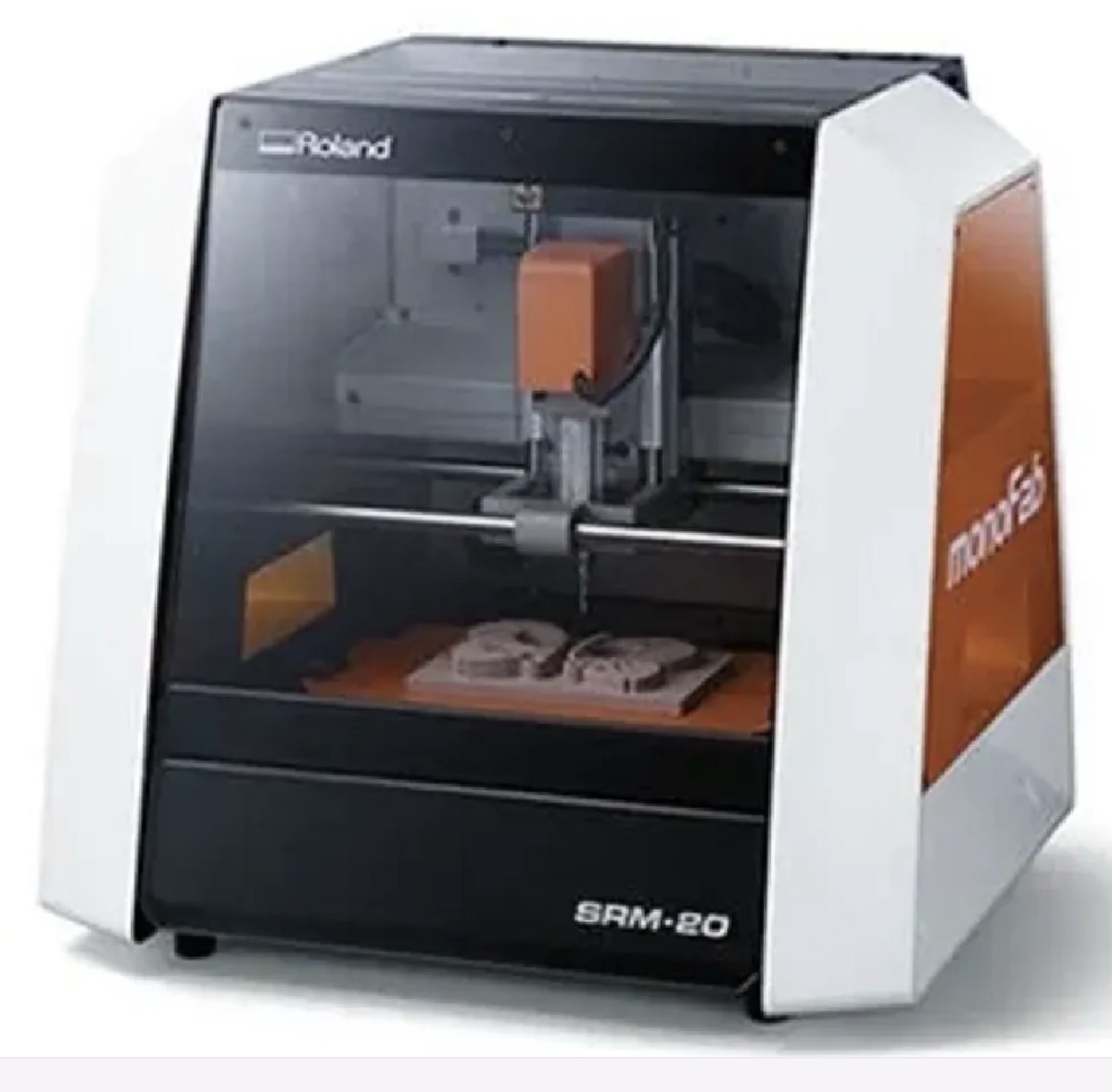
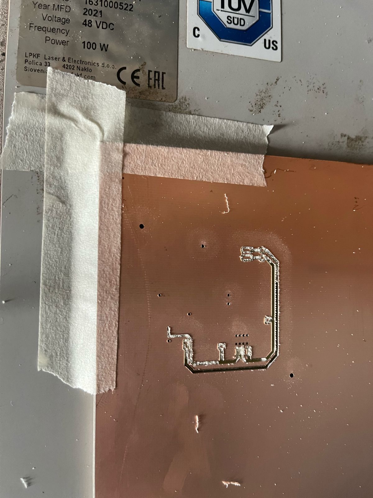
Machines in our Fab Lab
Our FABLAB has Roland SRM 20,and Protomat E44 but we did on E44 as Roland SRM 20 was a very old machine and since years no one has used it. To know more about Protomat E44 Circuit Board plotter click Here. For Roland SRM 20 click Here.
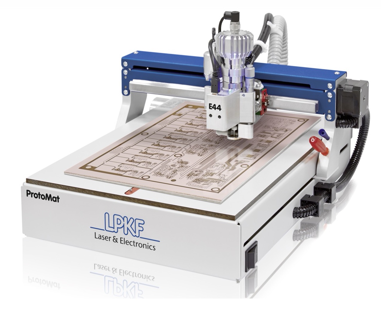
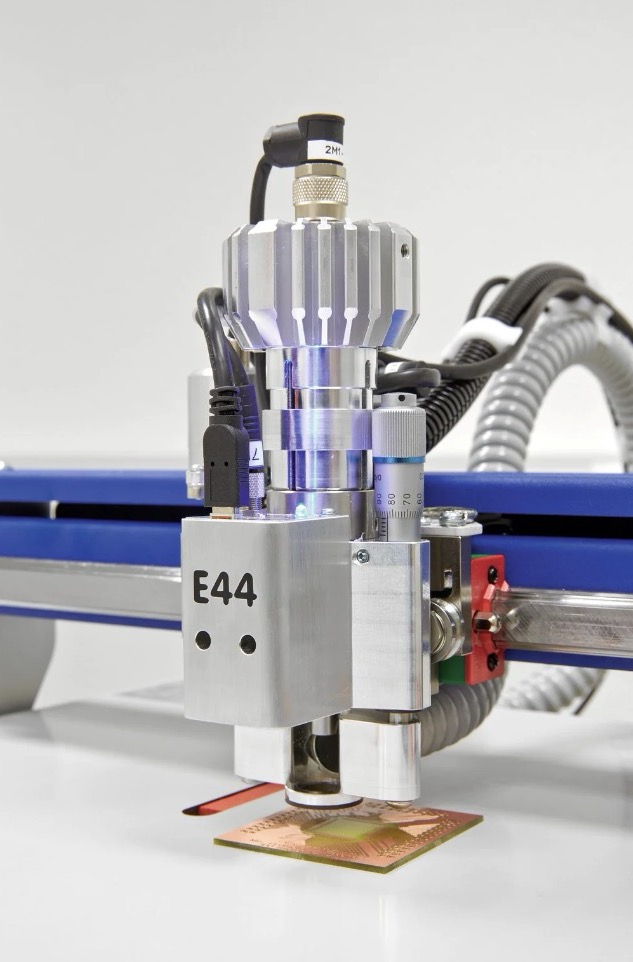
About Protomat E44
The LPKF ProtoMat E44 is the cost-effective entry into the world of professional PCB prototyping. The system scores with its particularly simple operation.
Features of the machine are:
1. LPKF quality at an entry- level rate
2. With powerful CAM software
3. Single and printed double sided circuit boards
4. Ideal for reserach and training
5. Safe, Precise and Affordable
Understanding the basics of Design Software
I thought before using the machine I should know at least the basics of the design software,or at leat the interface and tools in that software so that I get familiar to some terms which are safe in LPKM Circuit Pro PM software which will help me to relate more with the software and how to use the software.
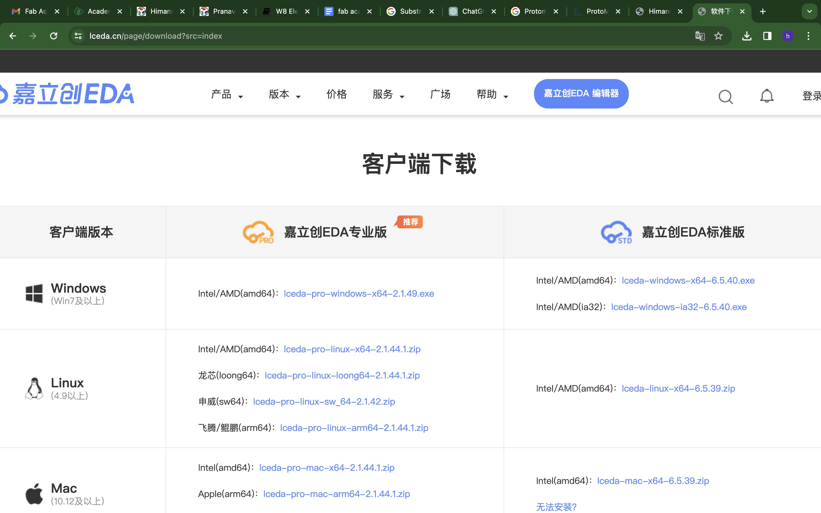
PCB design can be done on multiple softwares such as EasyEDA, Autodesk Eagle, KiCAD, etc. The first time my mentor showed me was EasyEDA software, I haven't designed anything on that software yet but was introduced to the basic interface introduction, tools and features in that software. I haven't explored other softwares yet but I got to know that one benefit in this software is that you can directly order the PCBs for printing/mass printing from the JLCPCB. To download EasyEDA software click Here.
As I have macbook pro I downloaded the apple version as shown in the image below:
The basic interface of the app looks like this:
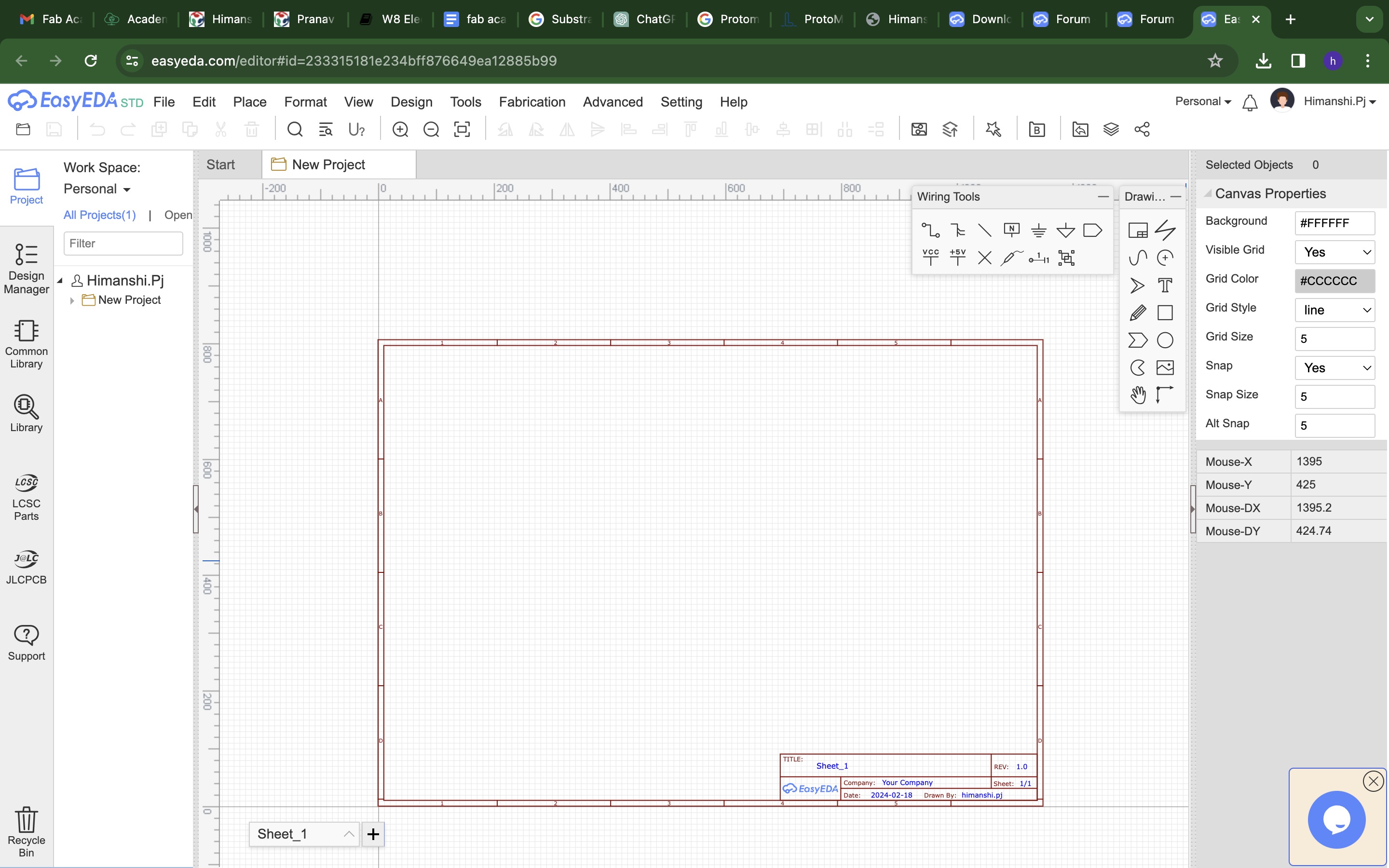
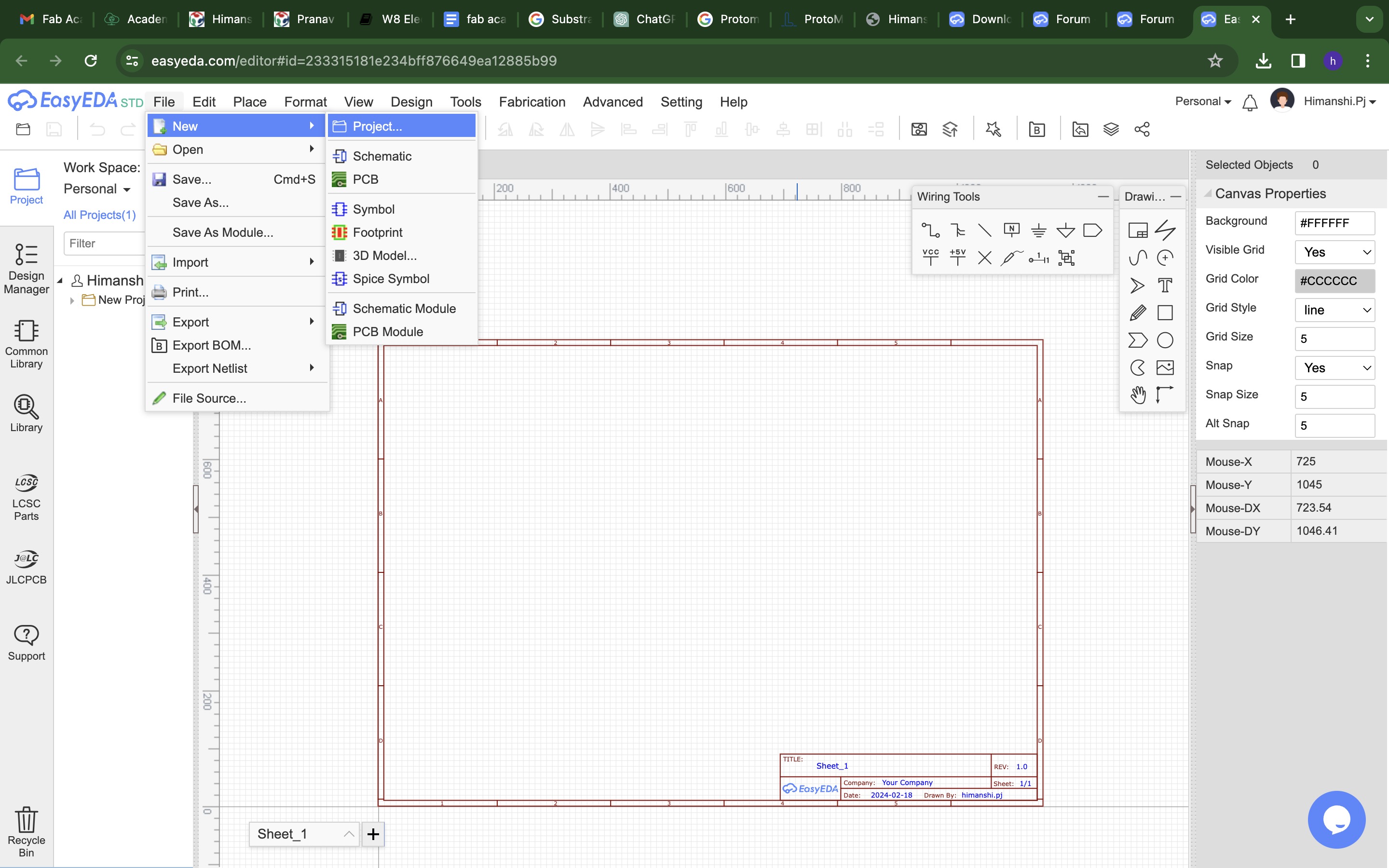
To start designing, FIle > New > Project. Then initiate a new schematic to start first.
To start importing electronic components, open the library panel and enter the name in the search window as shown in the figure below:
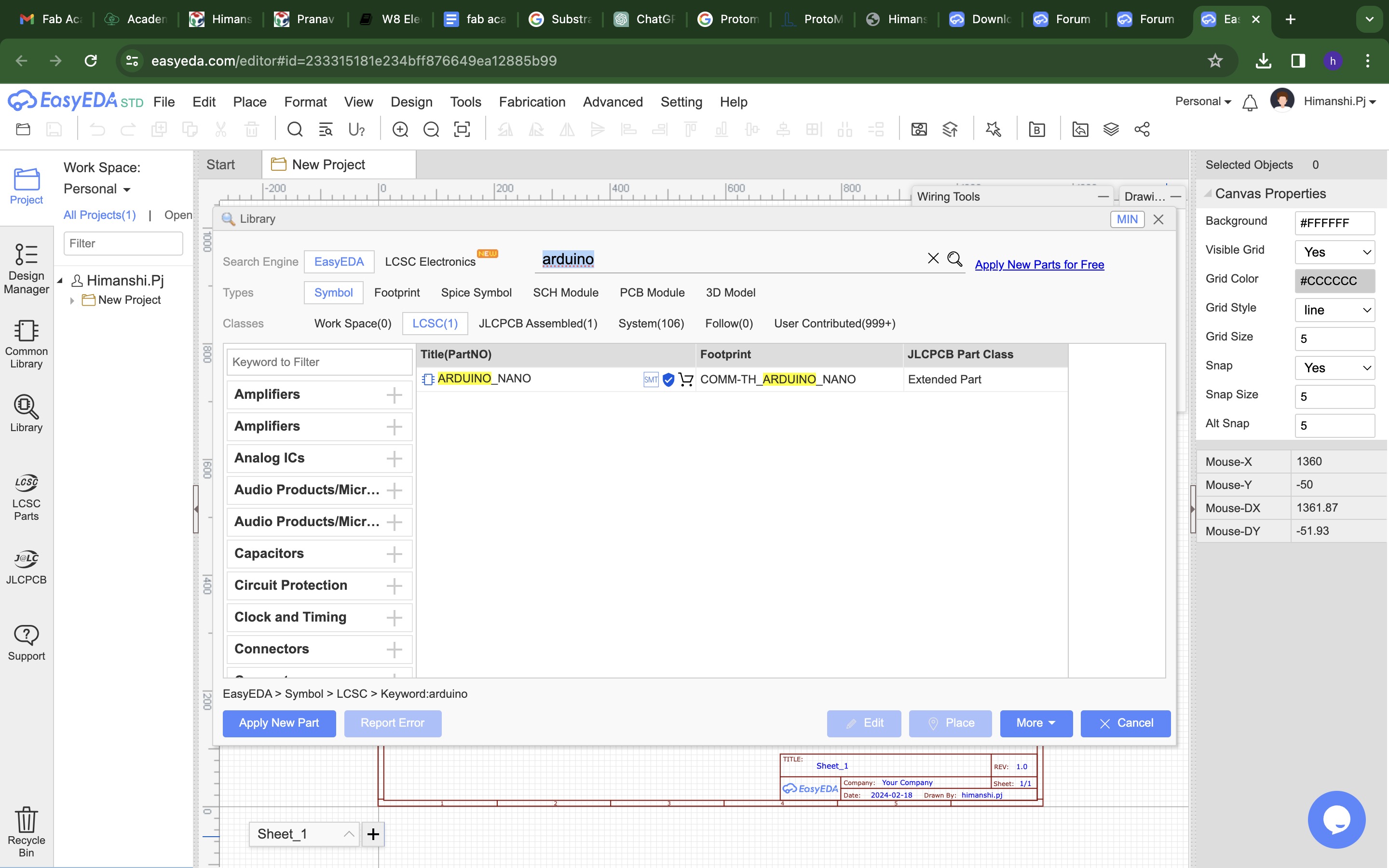
I referred to arduino uno custom circuit example online whoes link is Here. and started importing components accordingly from the library.
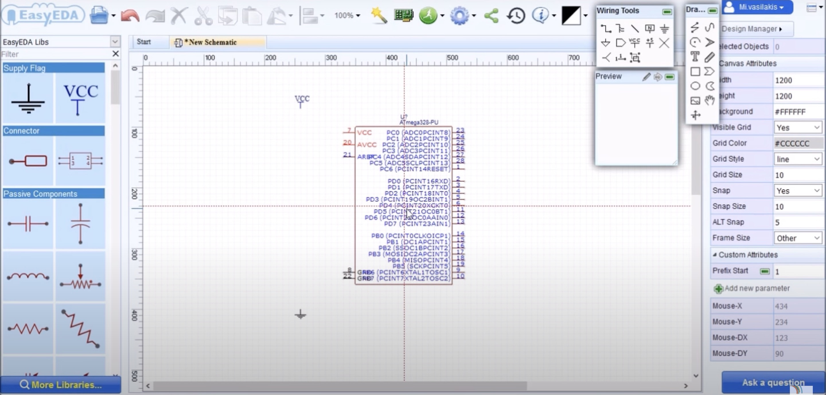
Once I imported all the necessary components, it was time to connect the wires in the schematic. You can do that using the top right panel in the interface as shown in the figure below:
Tip: Make sure to mark x on the ports that are not going to be connected to anything or it will show as an error.

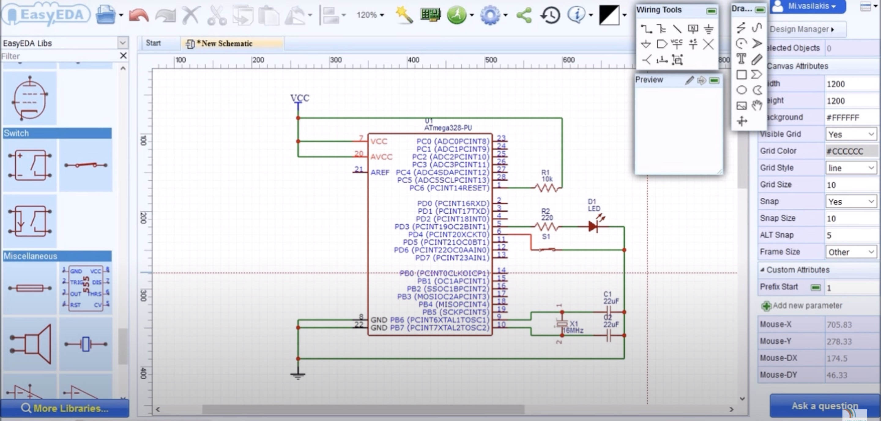
After all connections are made it looks like this:
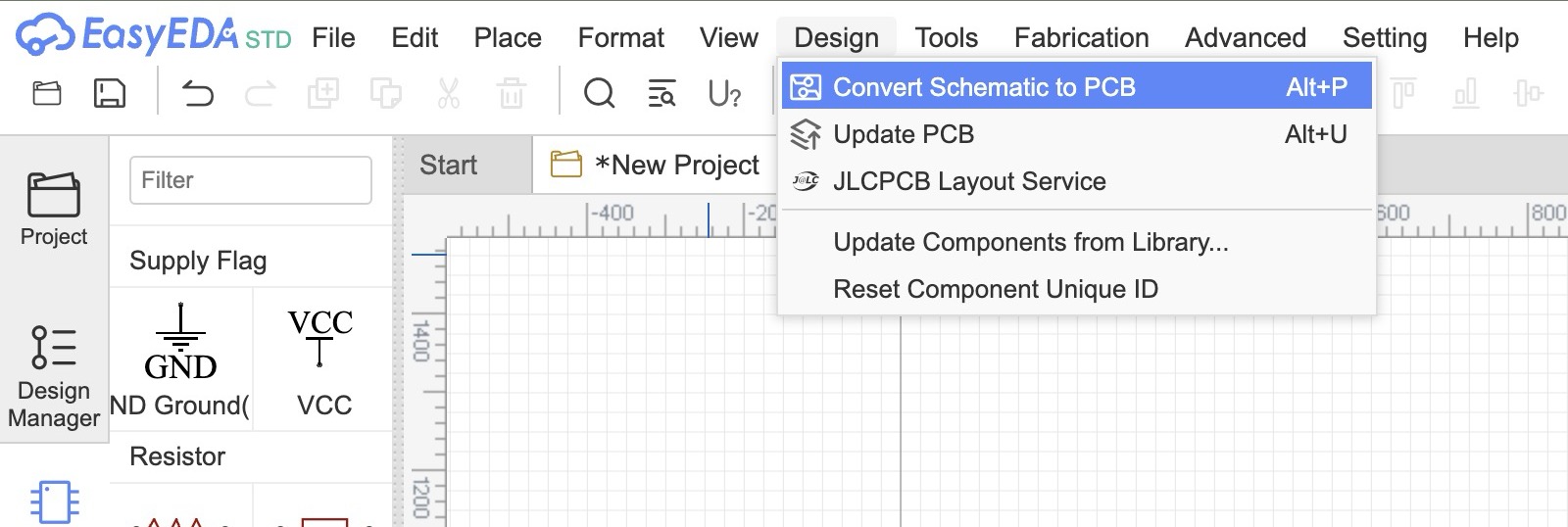
Once all the connections are done, we conver the schematic into PCB design. The steps are Design > Convert schematic to PCB or shortcut (Command+P)
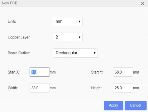
You can check nets before converting when the dialog box pops up. Once that is done, the following PCB design dialogbox opens to choose the parameters. You can keep to default parameters as EasyEDA sets right parameters anywhich ways.
I still need to deep dive more but for the start I have learned and explored this much.
Draft 1
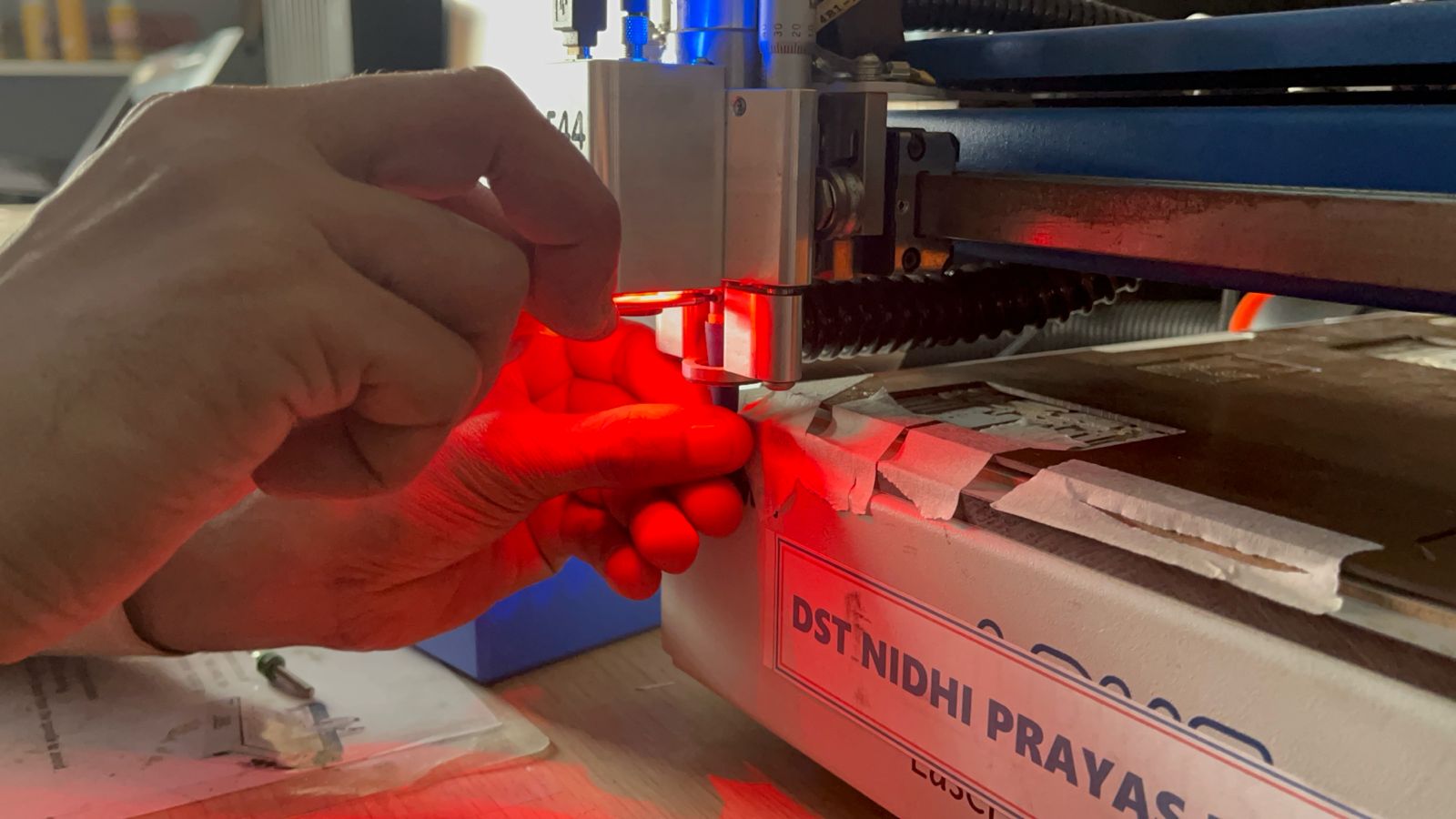
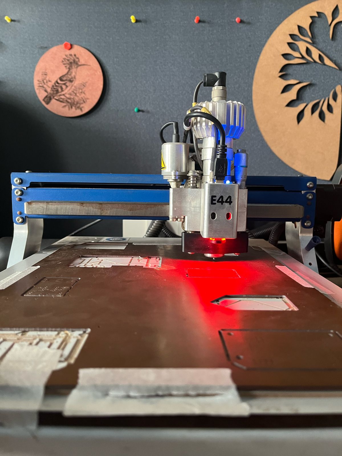
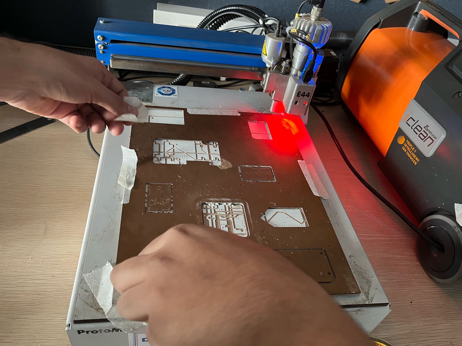
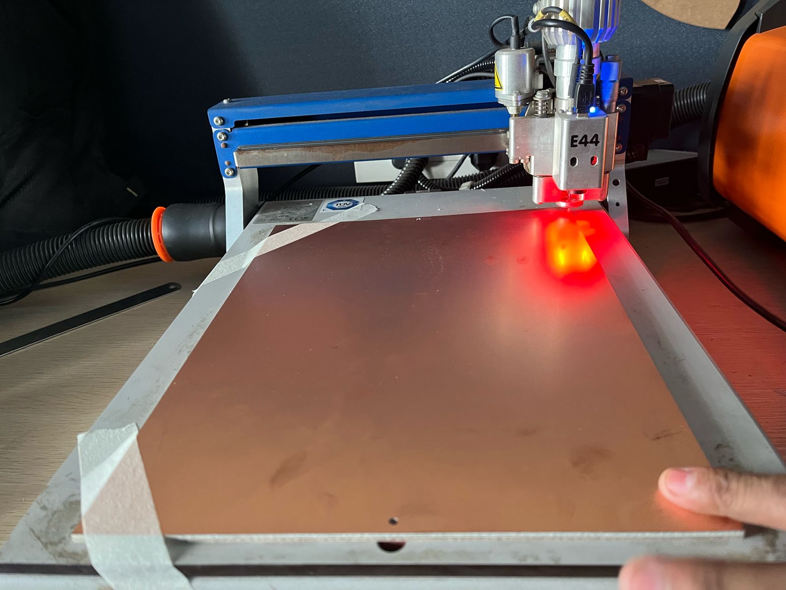
Using Protomat E44
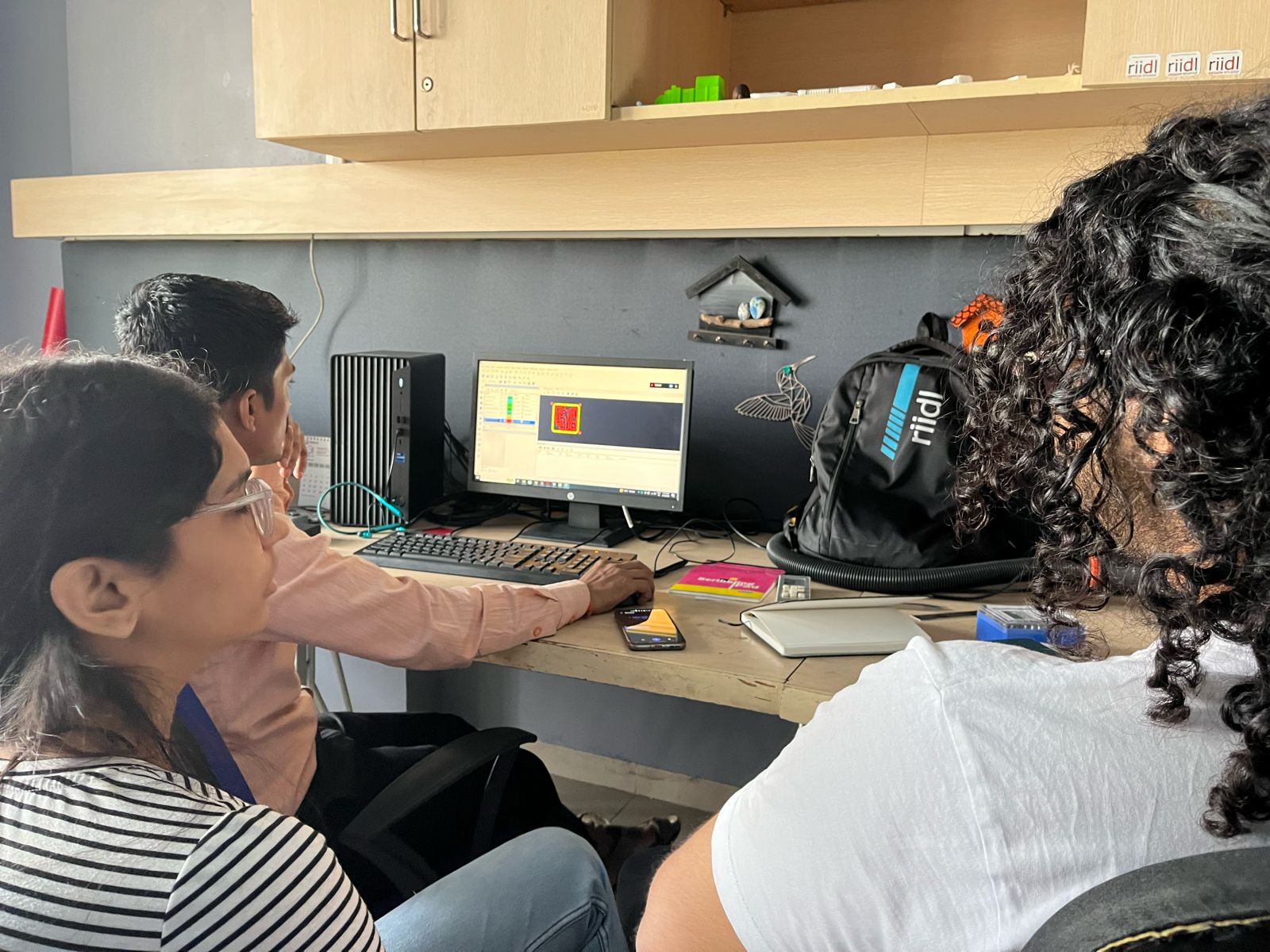
We started by knowing all the safety precautions and started learning the software first and then went on the machine
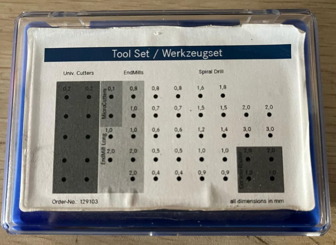
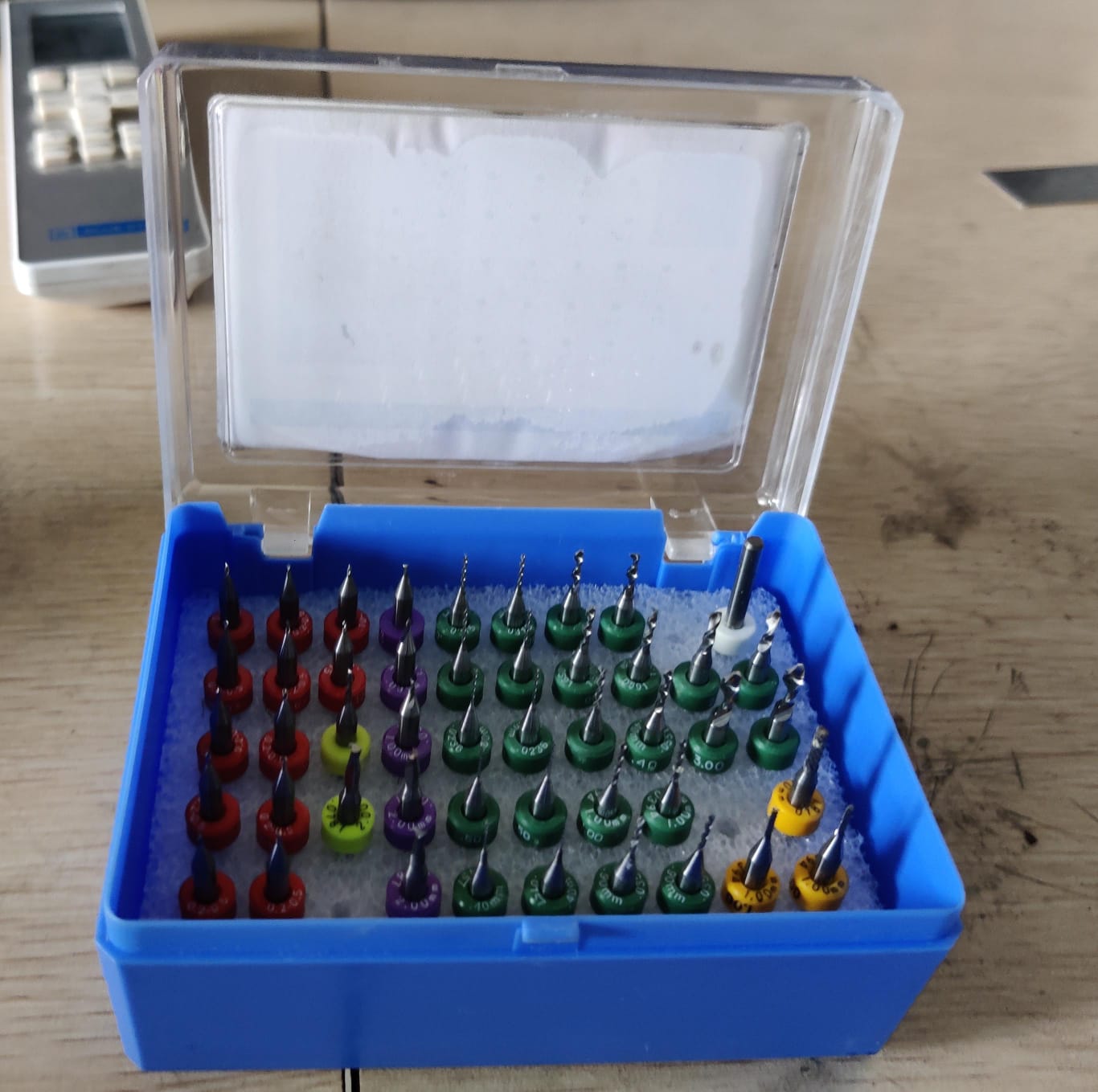
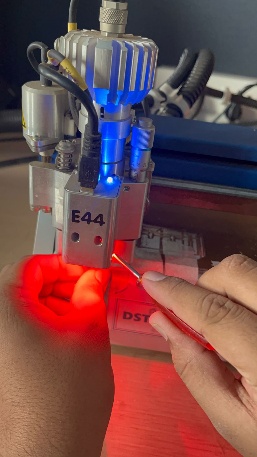
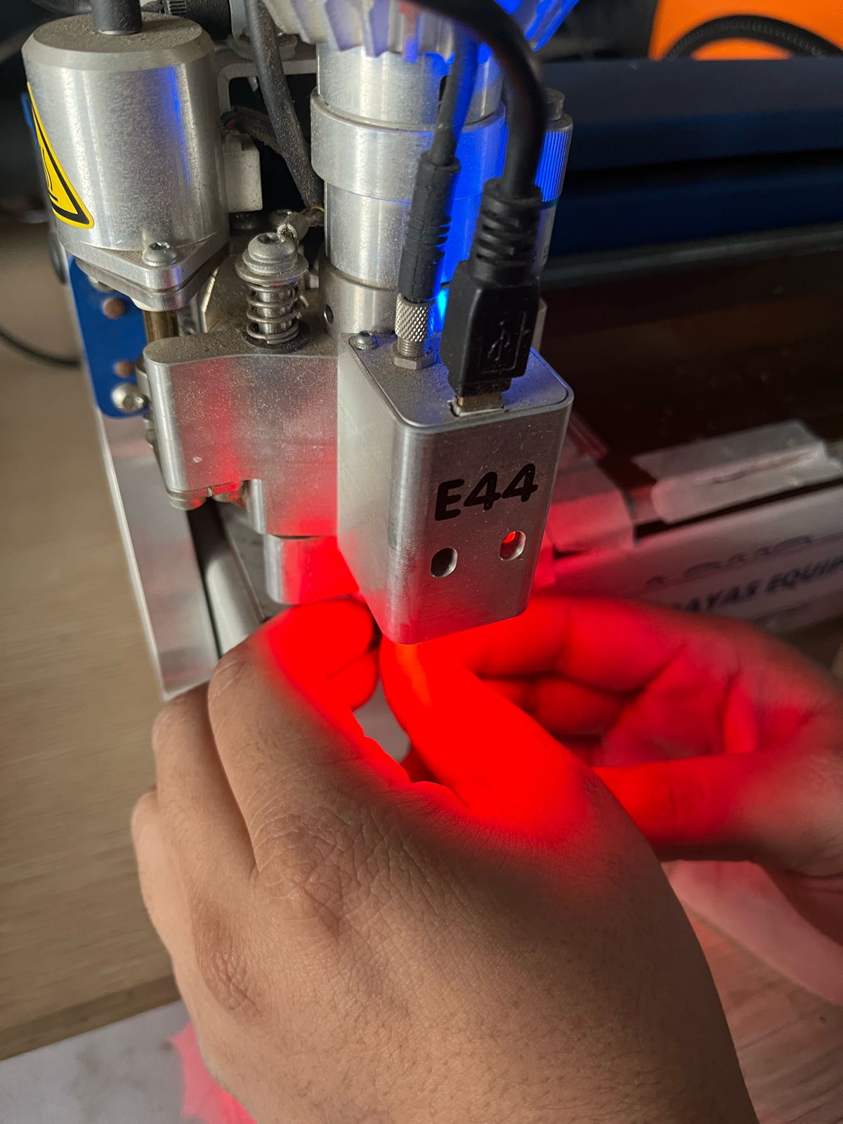
Along with the machine we get the software as well as the extensive toolbox which has multiple tools. So the toolbox includes universal cutters, endmills, spiral drill, Endmill Long, MicroCutter, Contour Router, you need to see which type and size of tool the software is suggesting and accordingly first check the tool and size on the box se the placement of the tool, open the box and remove that tool out. Always check the tool after removing because sometimes someone could have made the mistake of placing the tool and it won't be in the right order. The toolbox as shown below:
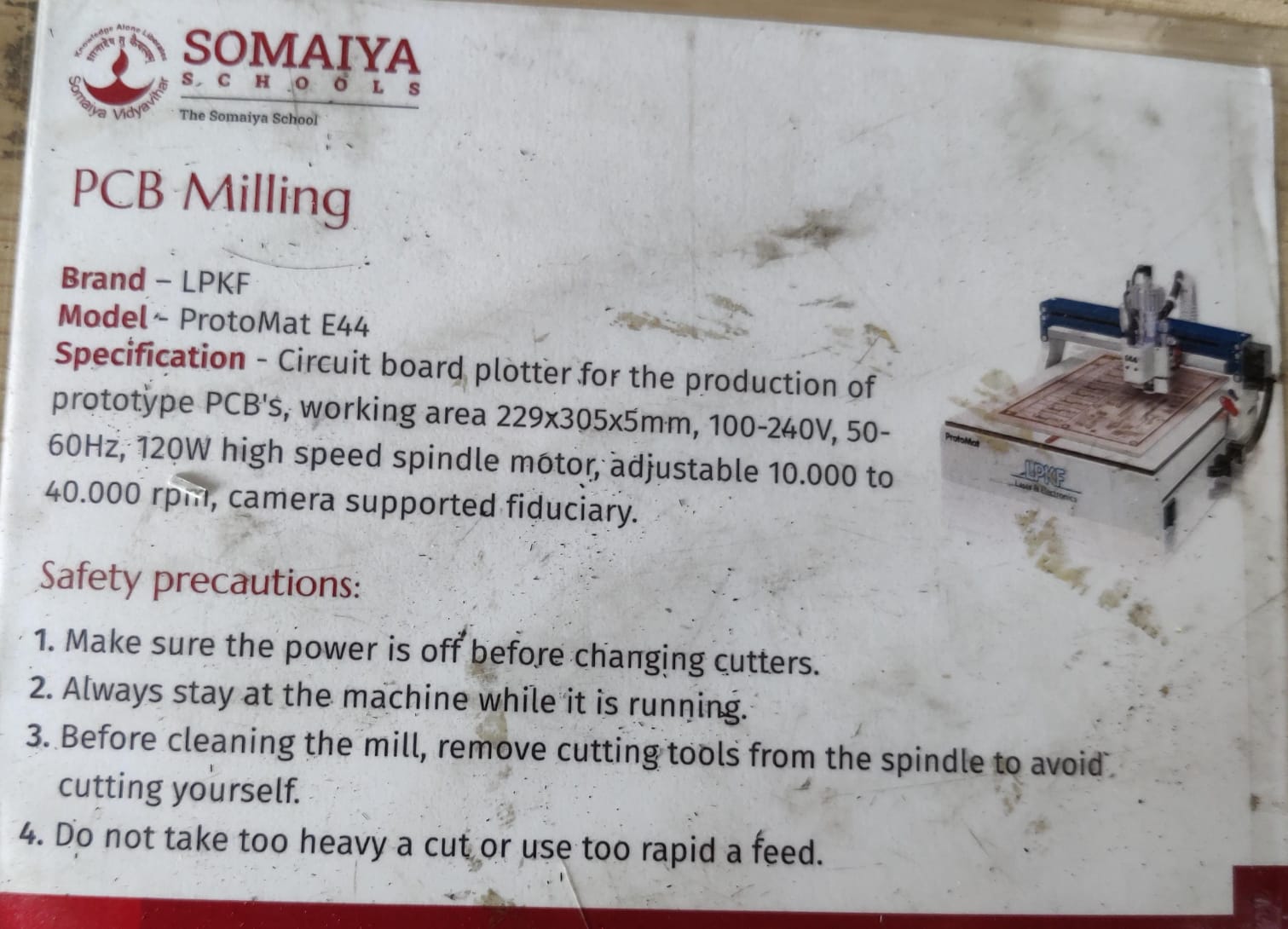
Step 01: Read and know about all safety Precautions
Besides every machine in our fab lab there is a safety precaution poster which we need to read and understand before starting that machine. To see the safety precautiojn for Protomat E44 see below:
Step 02: Installing LPKF software
The software you need to have installed on your PC for connecting with Protomat E44 is LPKM Circuit Pro PM.The installation process is pretty intuitive.The software includes supplied LPKF CircuitPro CAM software facilitates the solution of production requirements. It offers extensive access to all process parameters. A comprehensive parameter library for many common materials supports the operator in his own projects.
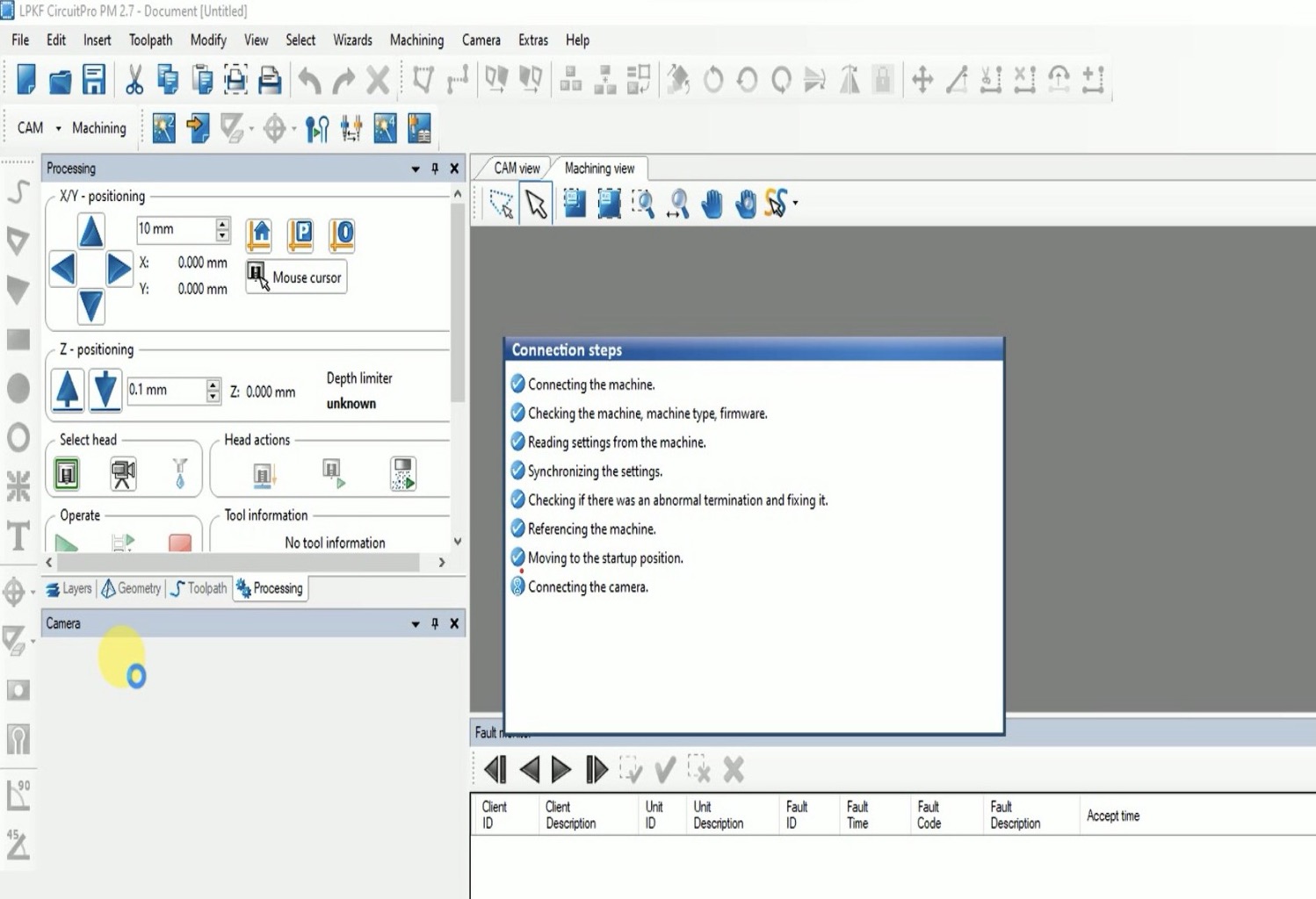
Step 03: Setting up the machine
Once the software is opne, it itself tries to find the machine (just make sure the machine is turned on and wired to the laptop) The interface looks as shown below and it takes few minutes to set up the machine, home the end effector and reference the machine overall.
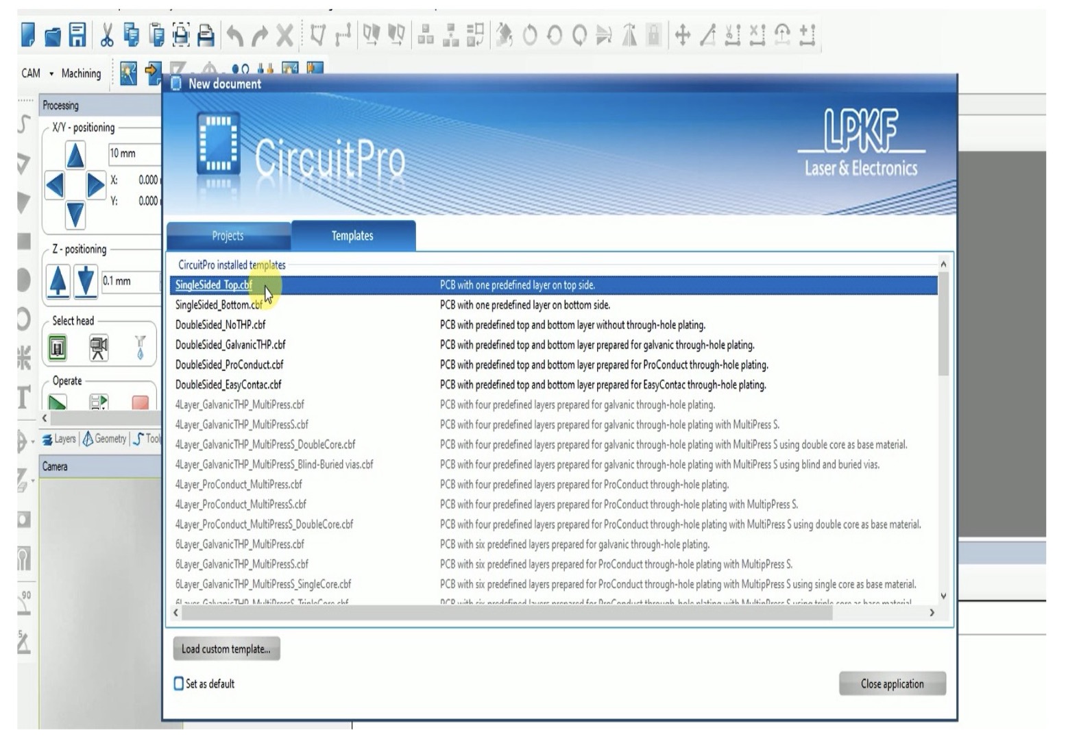
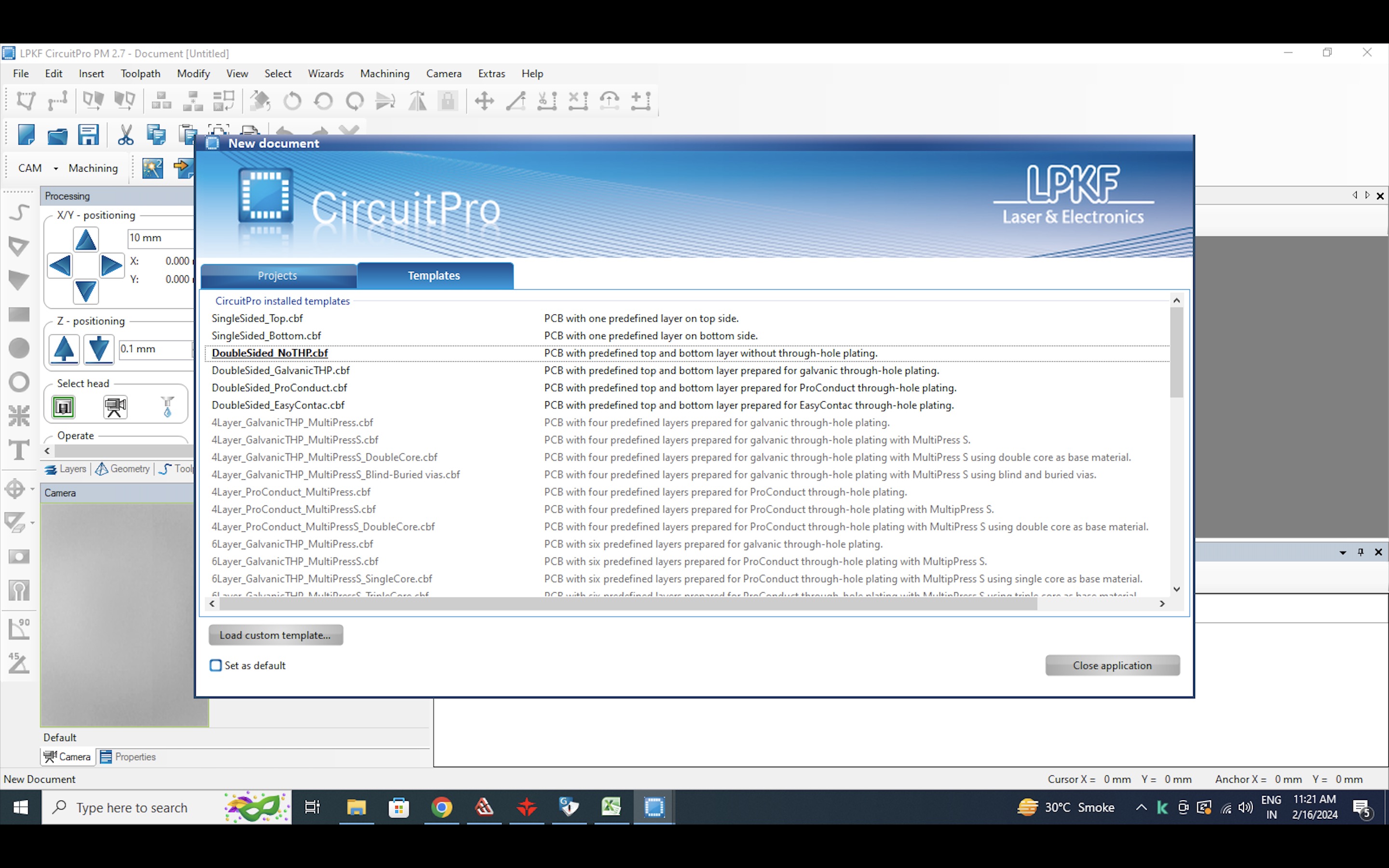
Step 04: Start a new document
Start a new document and choose the template based on the design of your PCB.
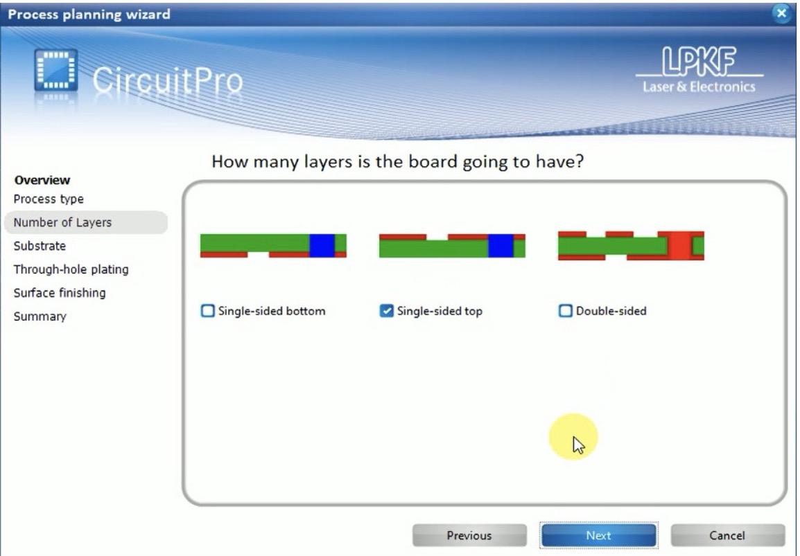
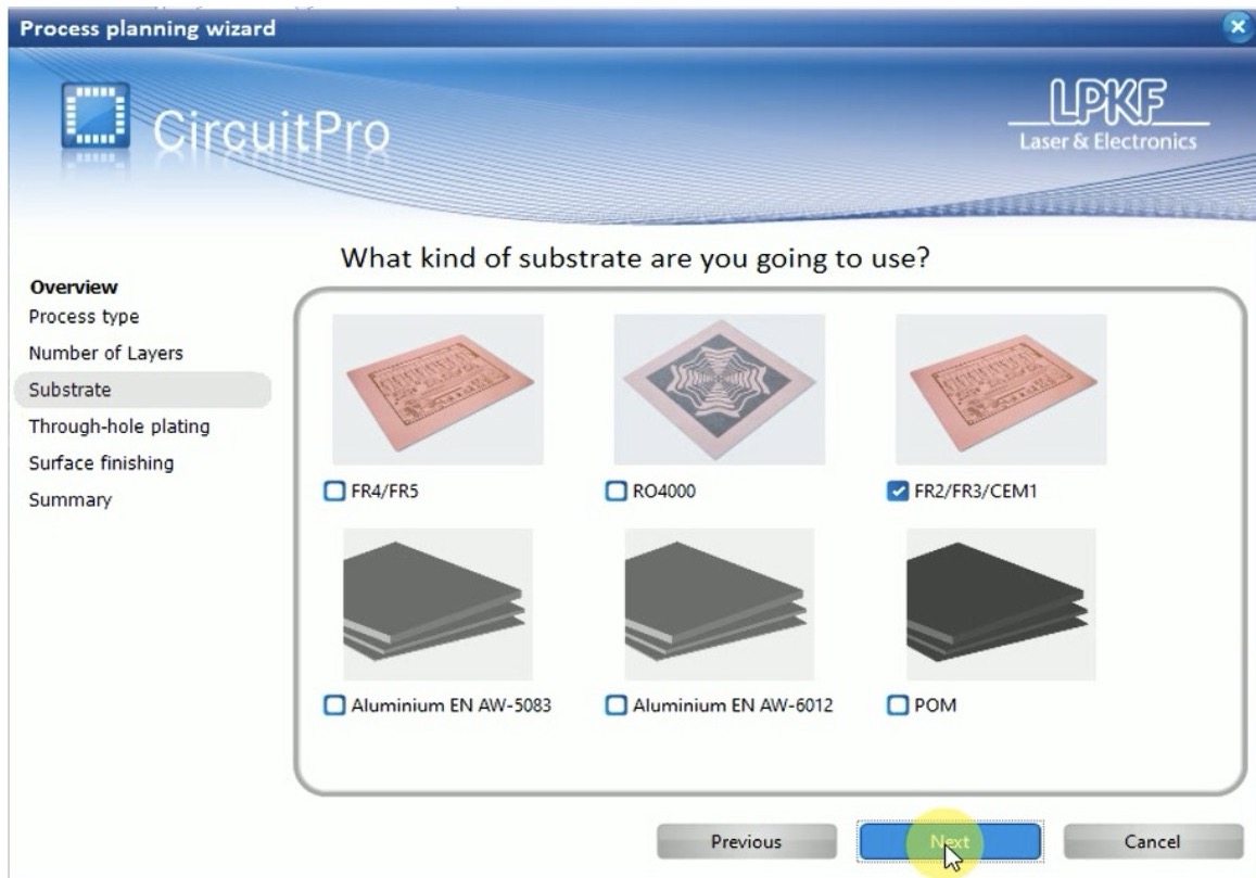
Step 05: Open process planning wizard
As shown below, open the process planning wizard.
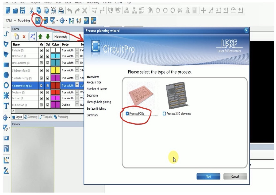
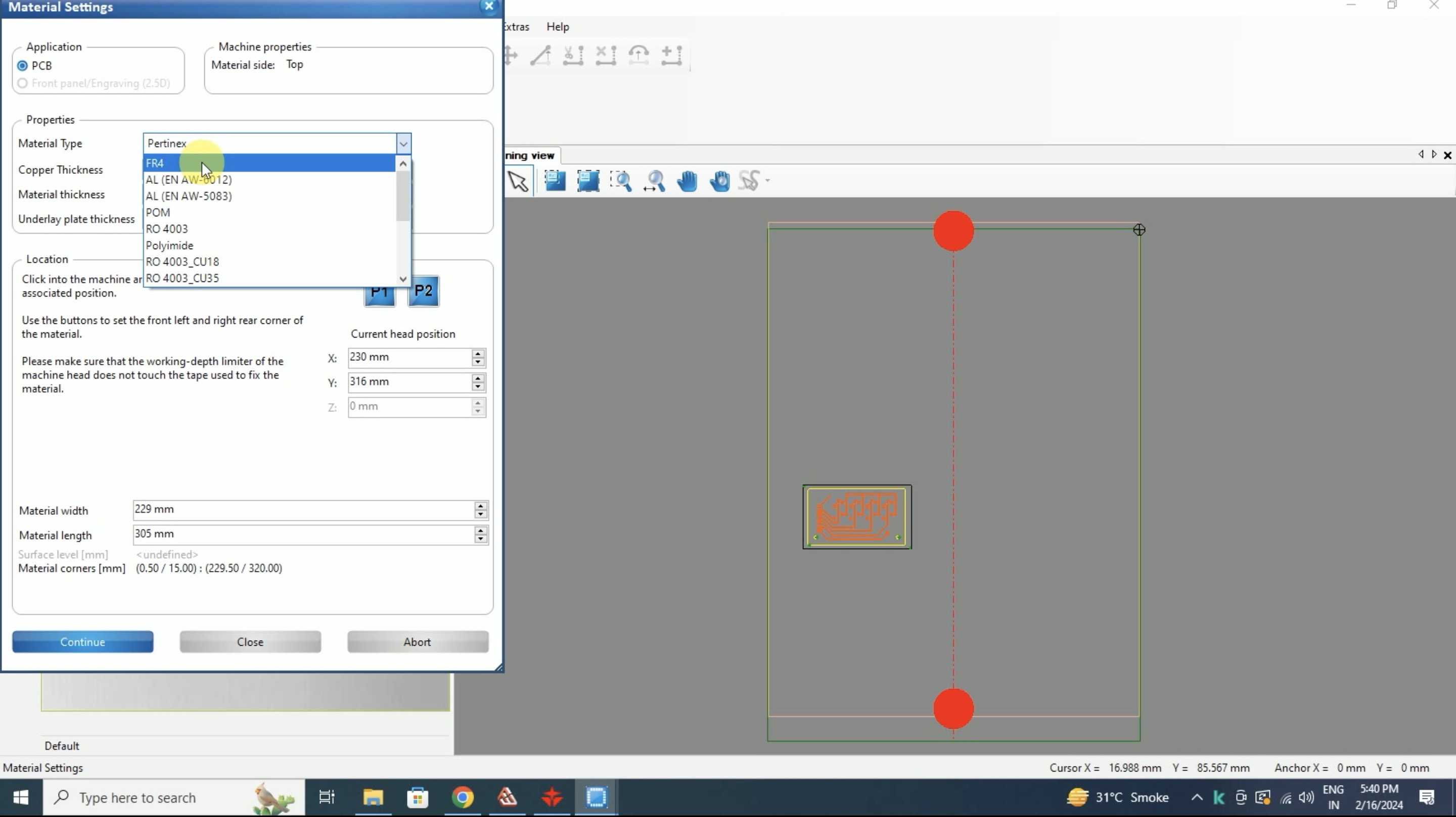
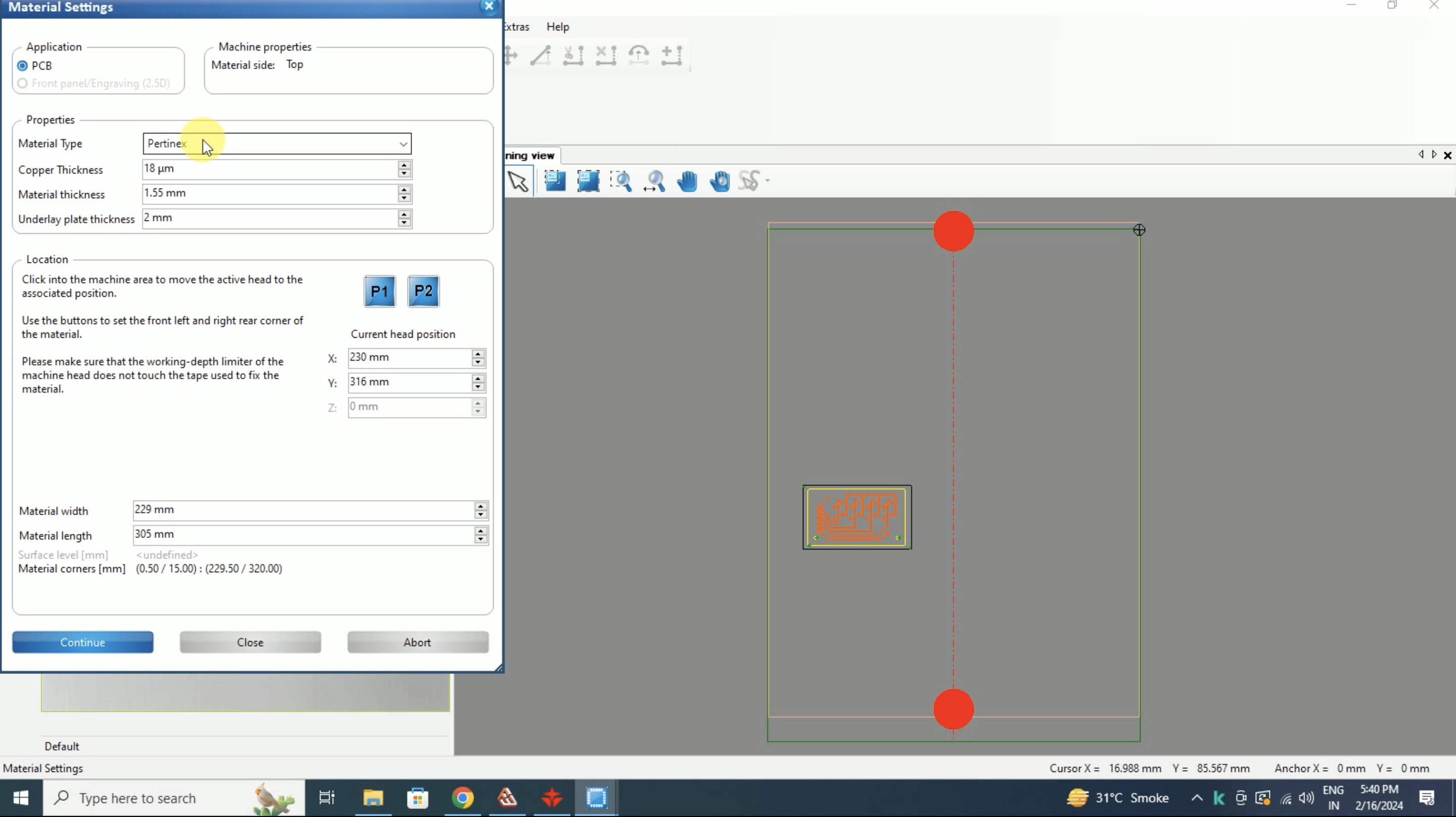
Choose the right options as shown in the images below for the process, single or double sided PCB, and substrate selection.
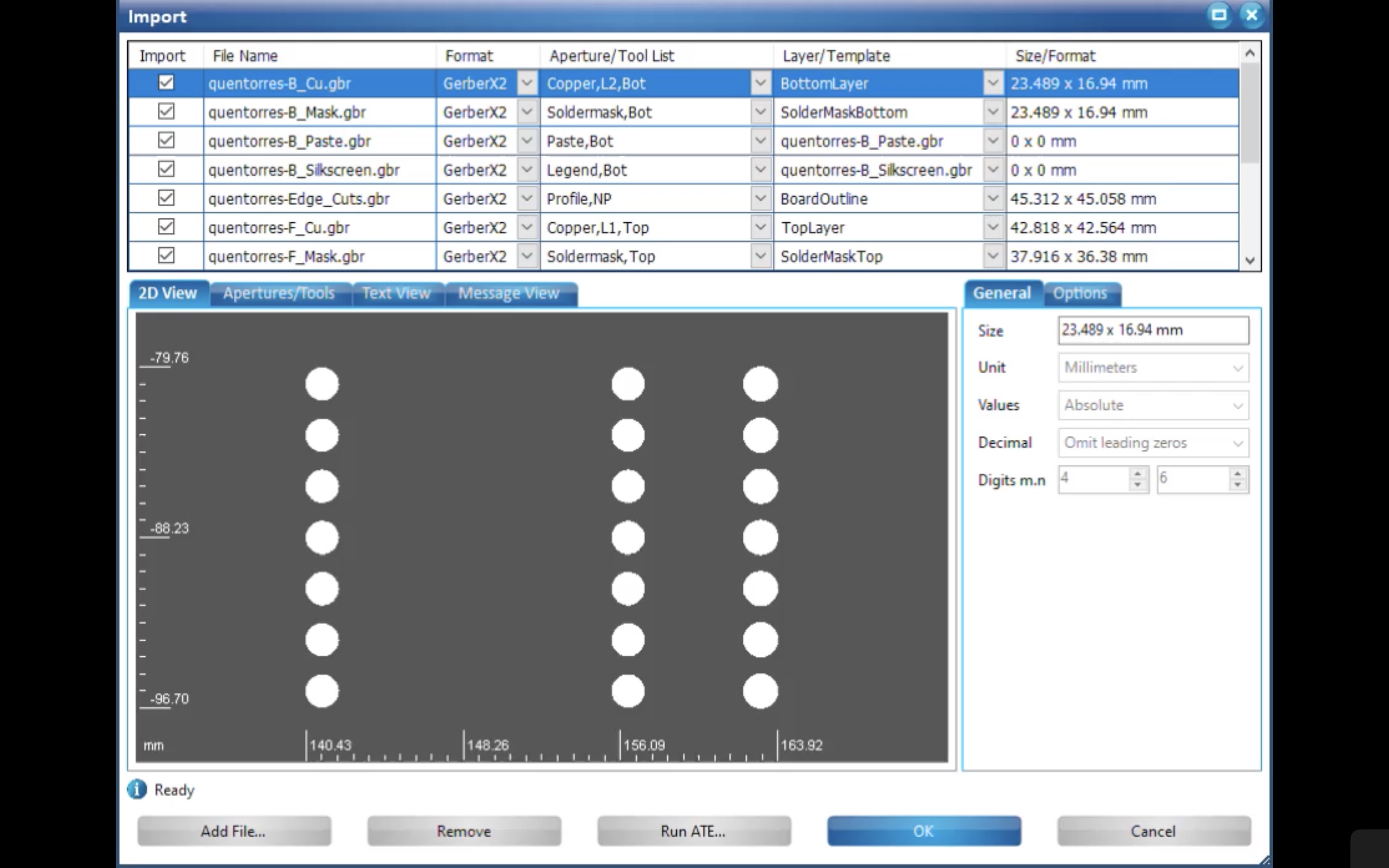
Step 06: Import Gerber file
Once that is set, go to files > import and then locate your gerber files and import them.
This is where we went wrong into properly selecting what exactly needs to be imported. We learnt it the hard way that, basically if it is a single sided PCB, you only need the following:
1. Boundary cut gerber file
2. Drilling holes gerber file
3. Top layer gerber file
4. And if you have a double-sided PCB design then we also need,
5. Bottom layer gerber file
6. Rest all silk screen layer, solid and paste masking layers are not needed for this process.
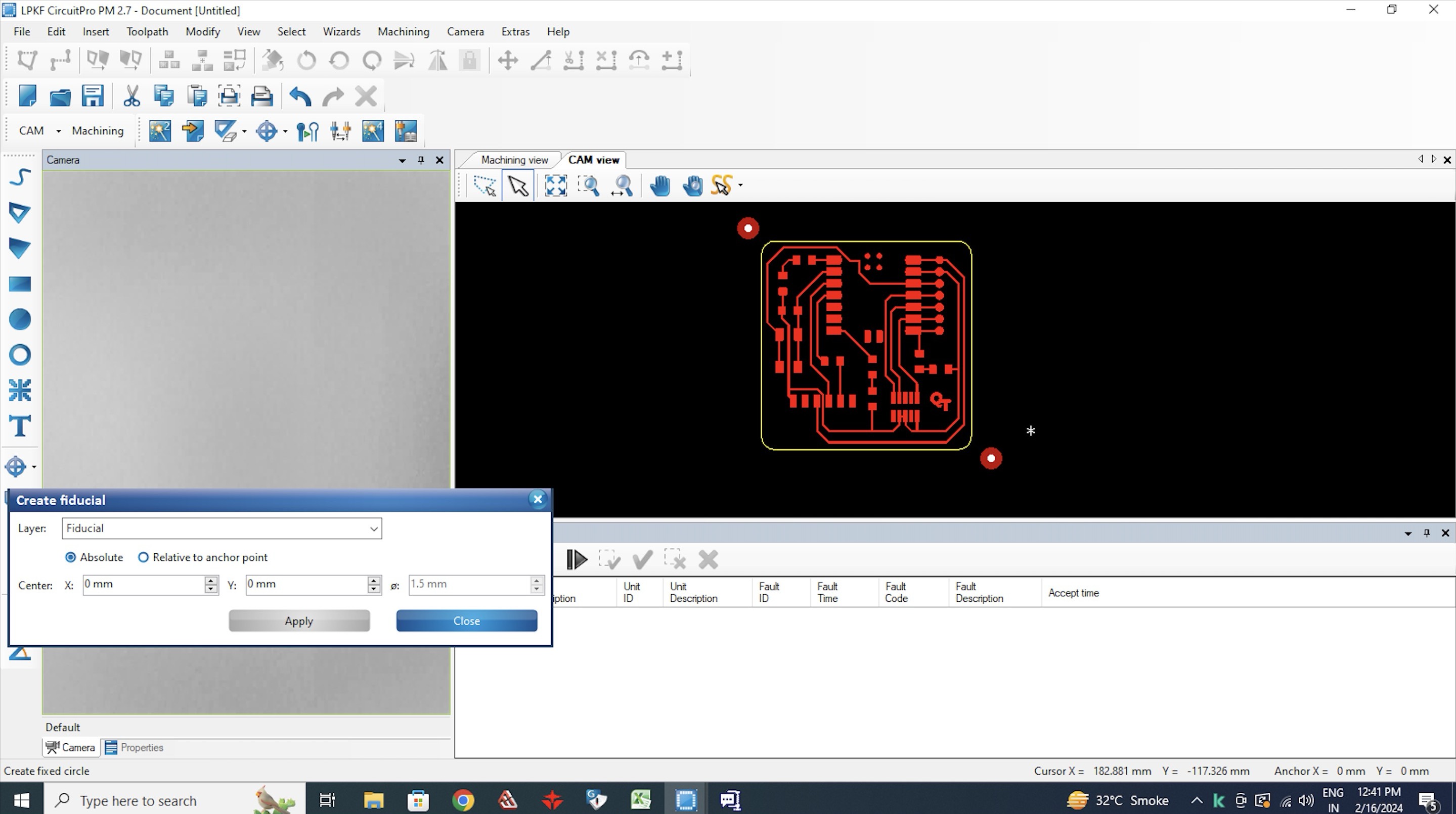
Step 07: Create fiducials
Now you need to define the end to end diagonal marks as fiducials to limit the space claim of the design on your copper plate. THis can be done as shown below:
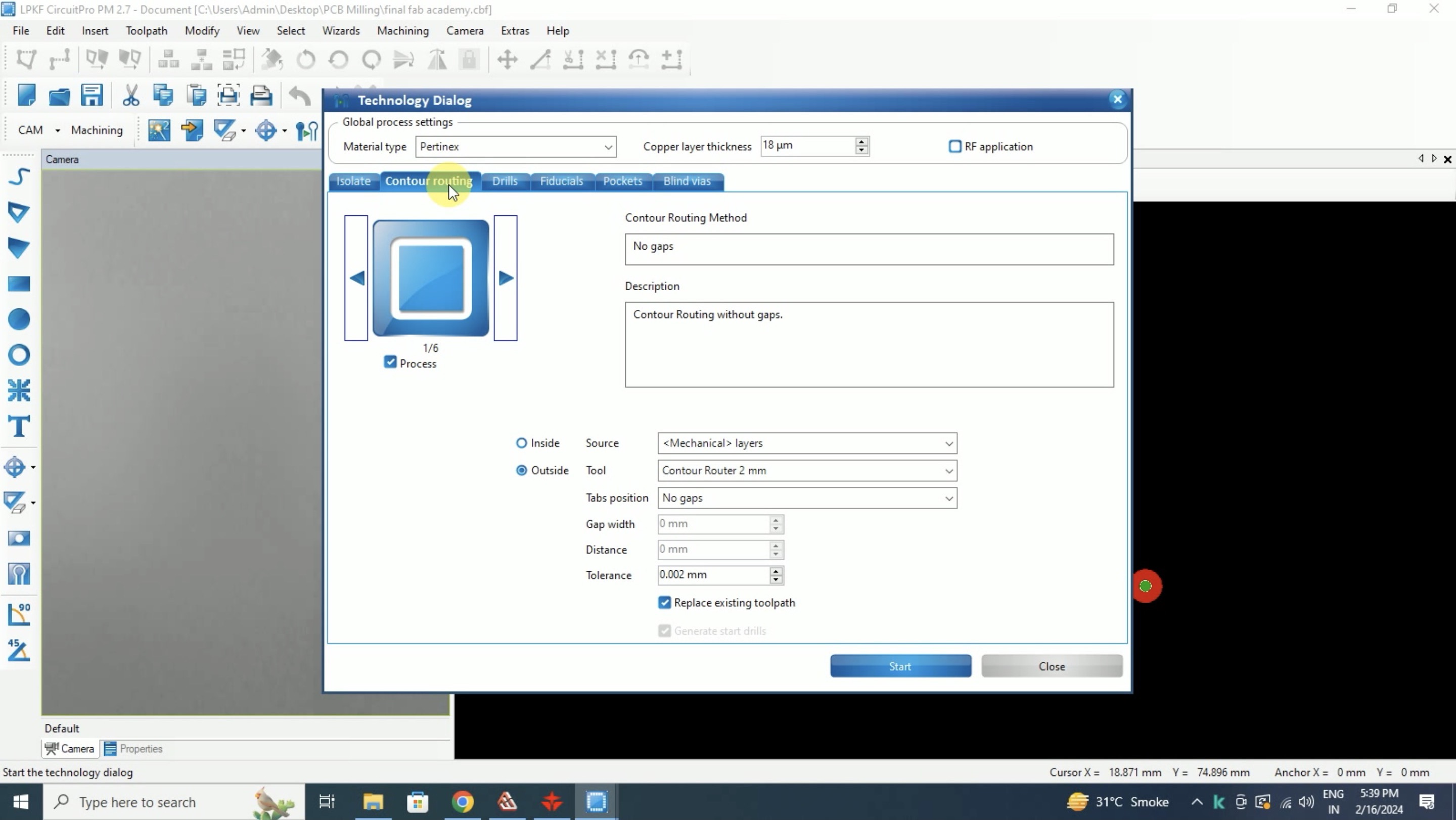
Step 08: Generate isolation and contour routing
Open the dialogbox as shown in the figure below. Here you need to define the isolation type, width, and number of channels. Very important steps. So basically this is where you define how muh isolation you want between two conducting lines.I kept it default for now as it was my first time I was usng it, I decided to chnge it after trying soldering on the first piece, so I will get an hint what measurements is best for me.

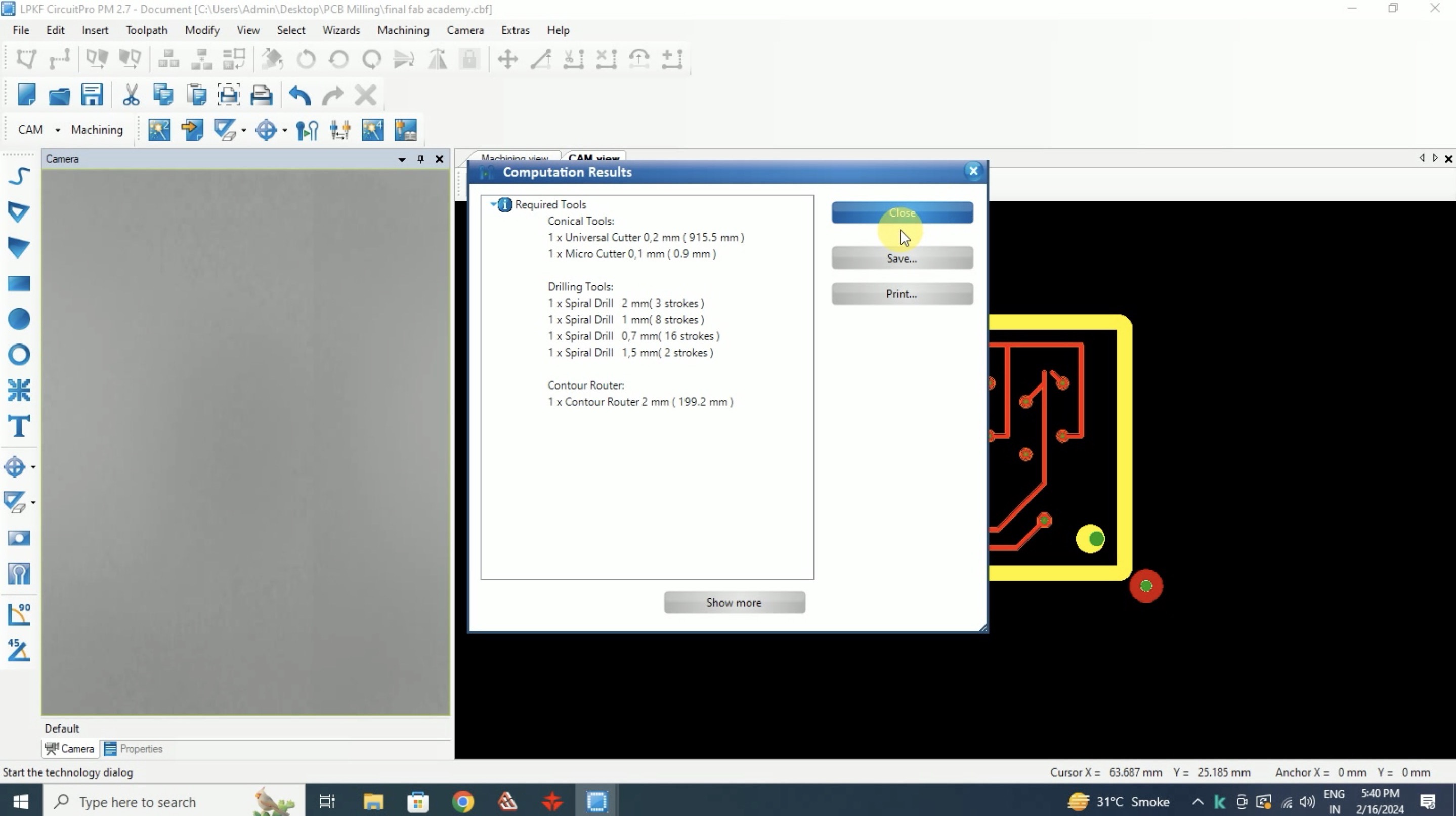
Once this all is setup and we click next, the overview of the types and number of tools are needed is showcased as shown below:
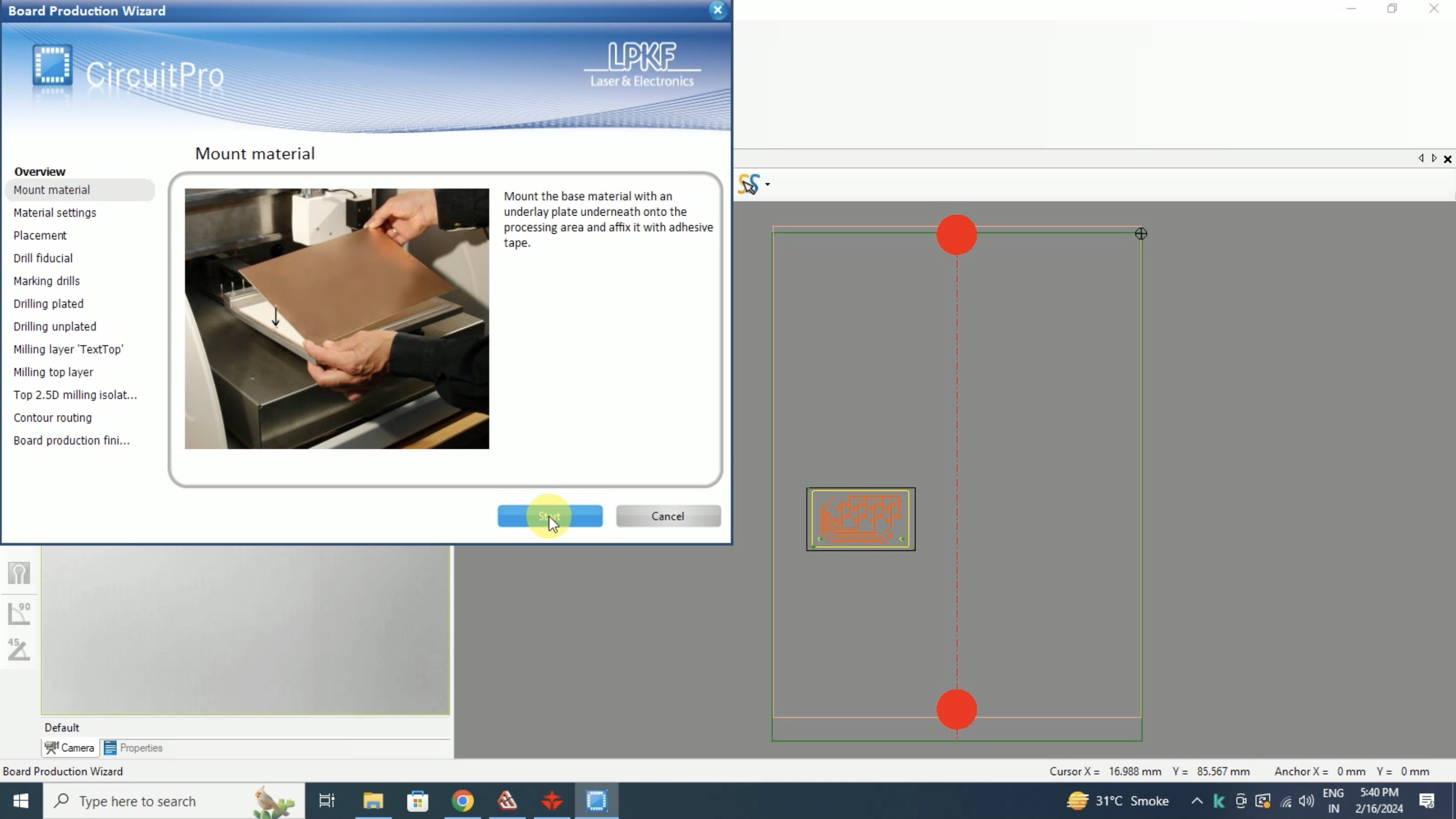
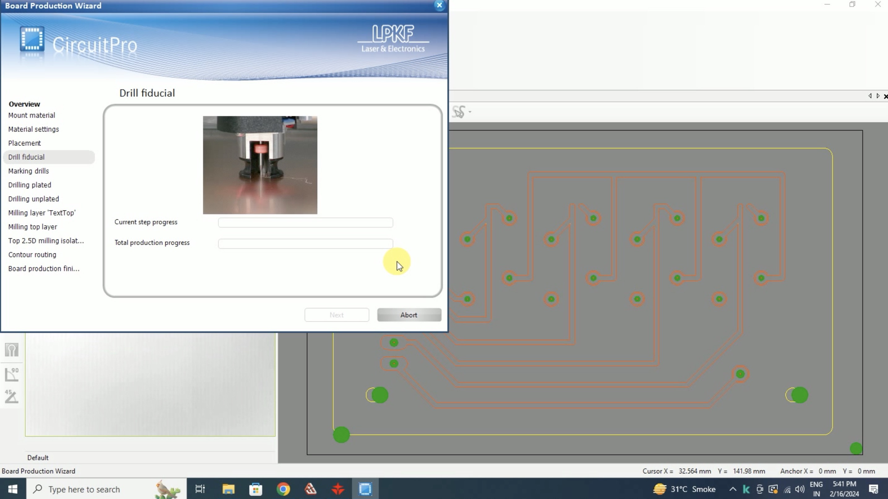
Step 09: Start board production wizard
Once everything is set, we start the board production wizard as shown in the figure below.
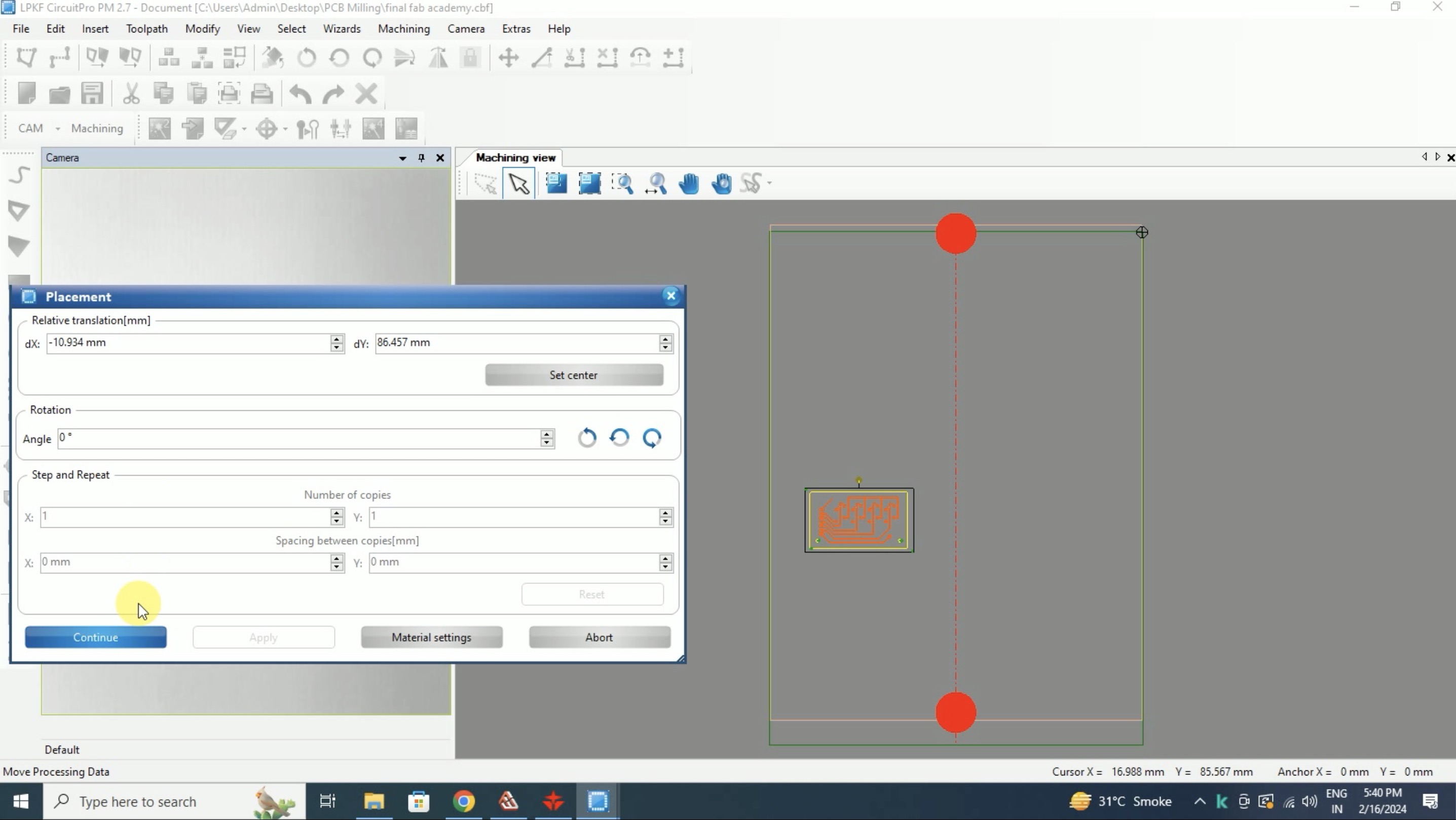
Step 10: Define PCB placement
To define the placement of the PCB on the copper plate, we go to Machining > Placement and then just drag and drop the rectangle define dby the previously marked fiducials to the desired location on the copper plate.
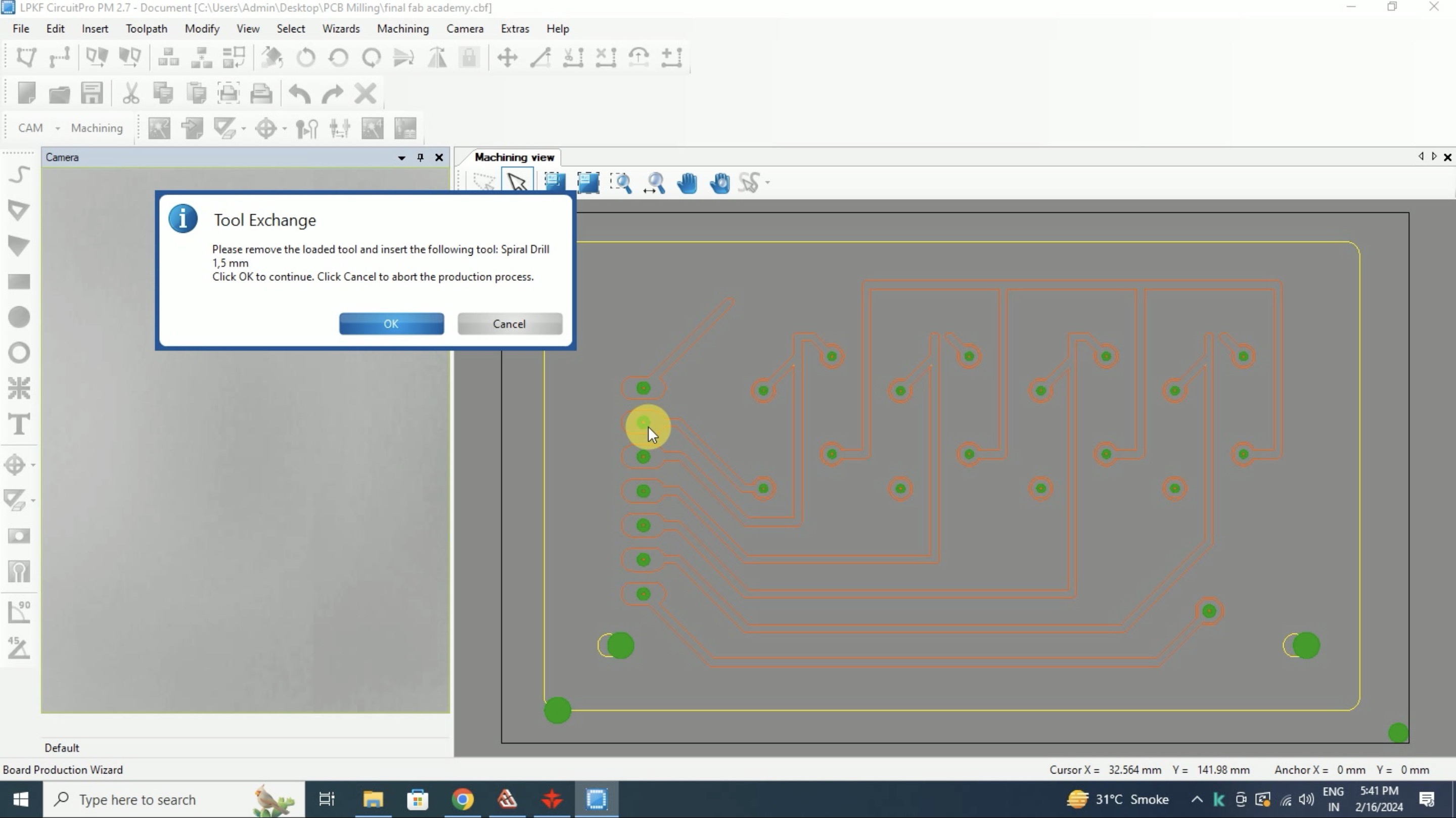
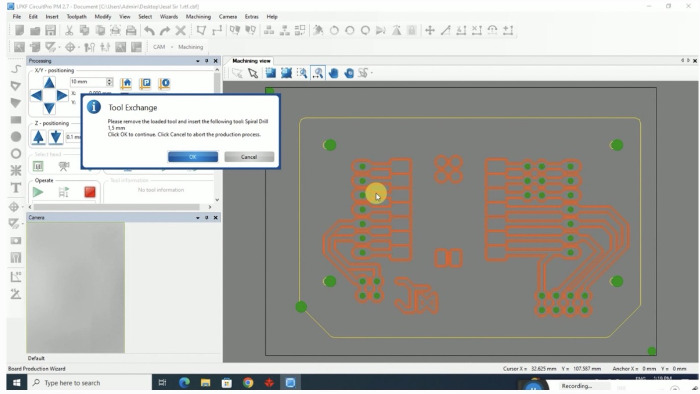
Step 11: Drill fiducials
Now the machine drills fiducials and also mentions which tool to mount for this action.
The stages and its tools used are listed below for single sided PCB (last iteration of mine)
Step 11a.: Fiducial hole marking
Tool: Spiral Drill 1.5mm
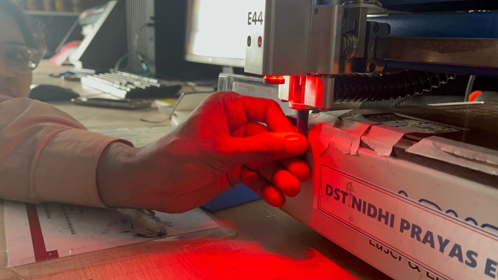
Accordingly we change the tool as shown below:
This step involves marking the end to end diagonal holes to define the boundary of the job
Step 11b. : Marking
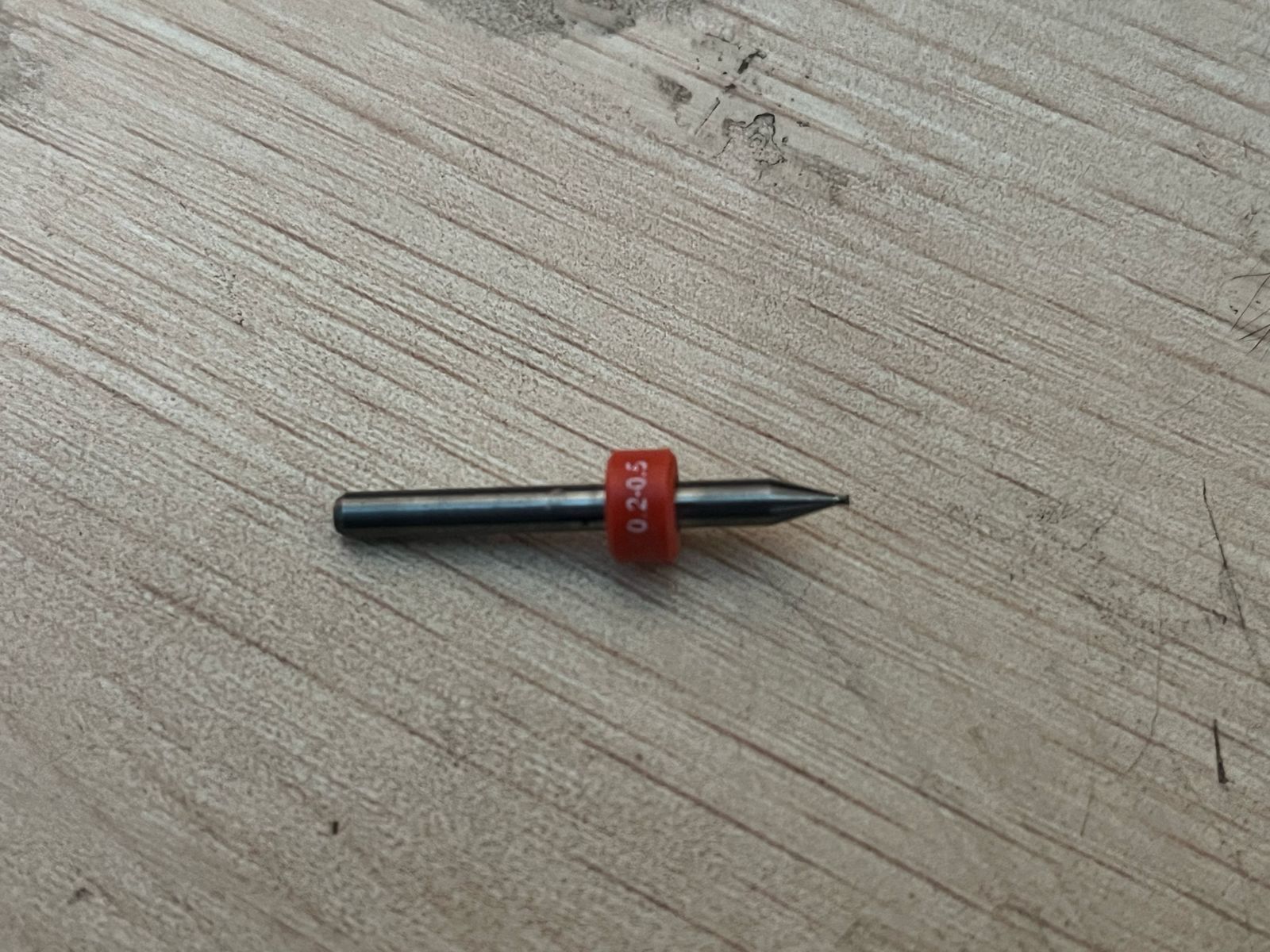
Tool: Micro cutter 0.1mm
This step involves the marking of all drill points, and crucial starting point for top layer milling
To see the video of working of the machine and changing bits, click below
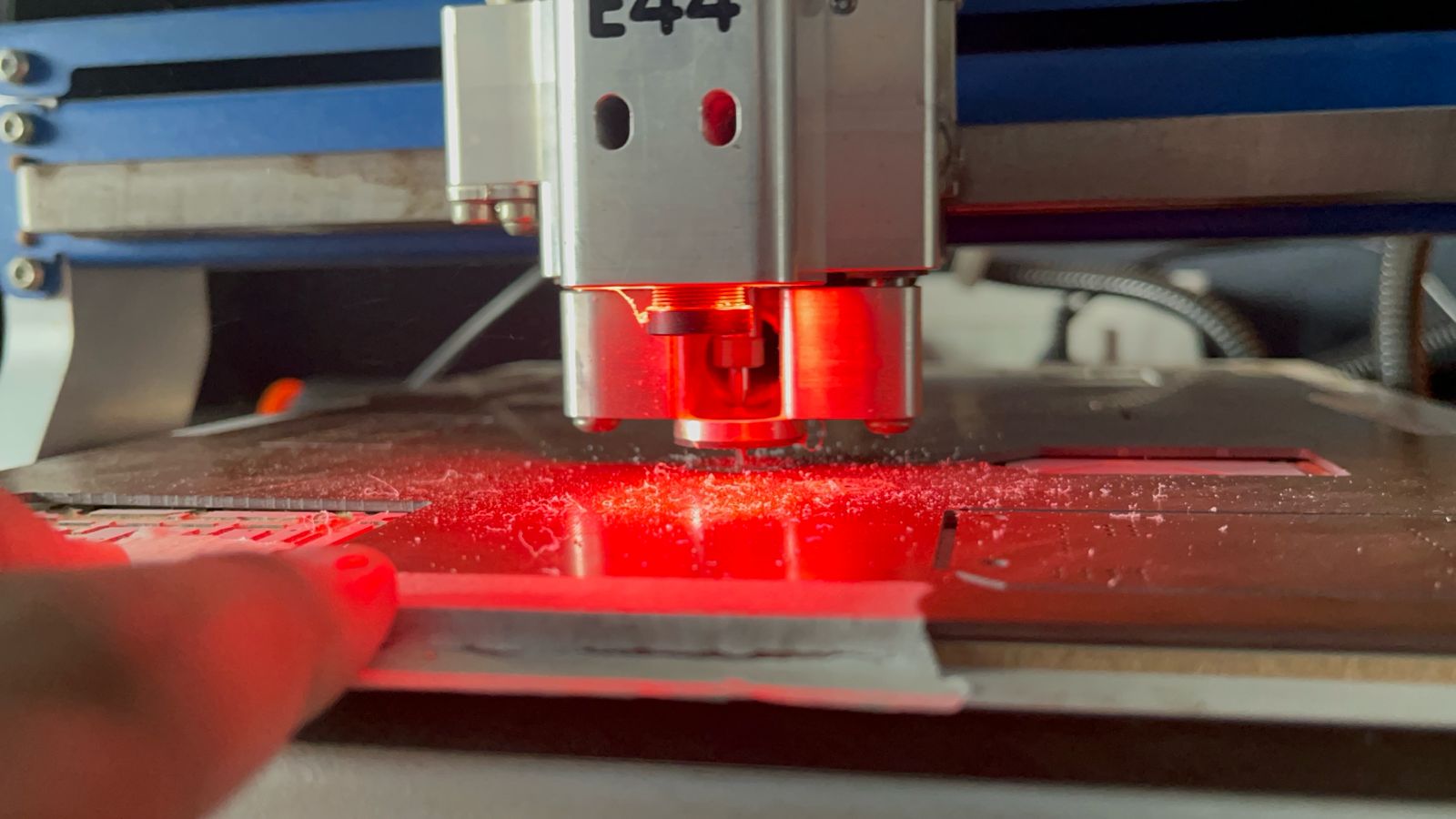
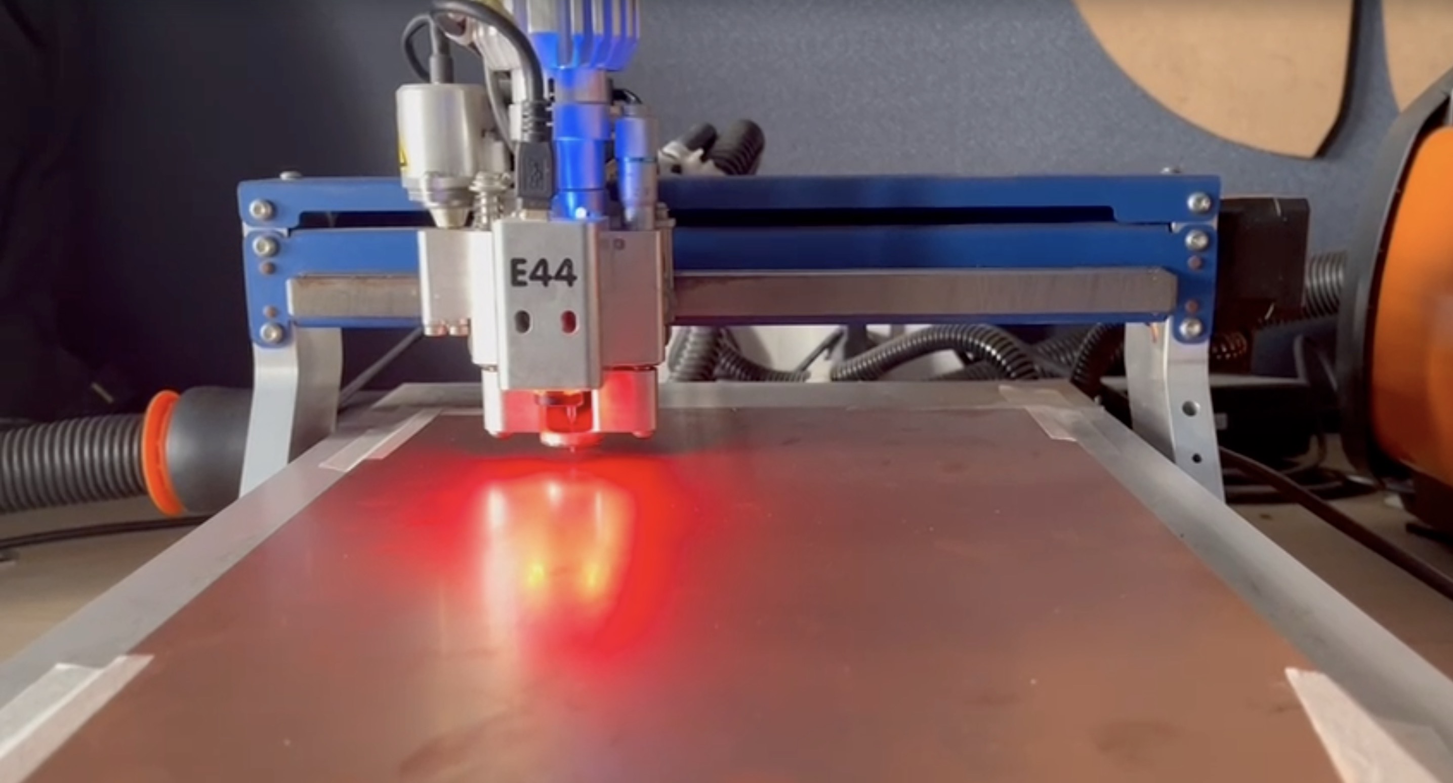
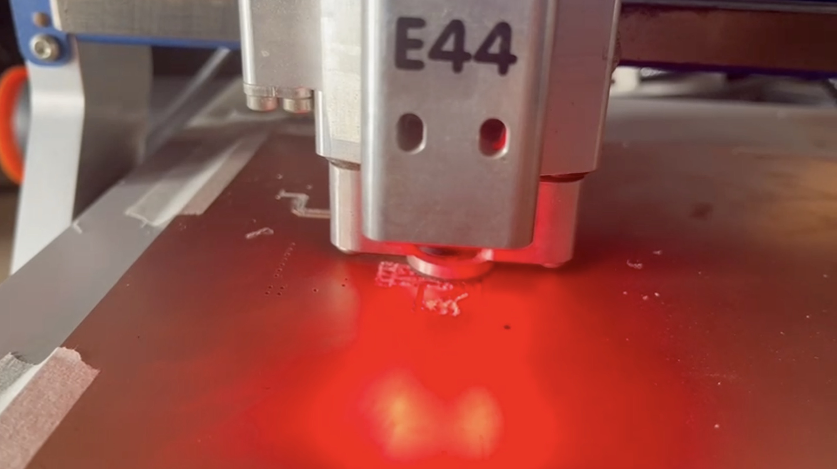
Step 11c : Milling
Tool: Universal cutter 0.2mmm
This step involves the actual milling of the 4 channels
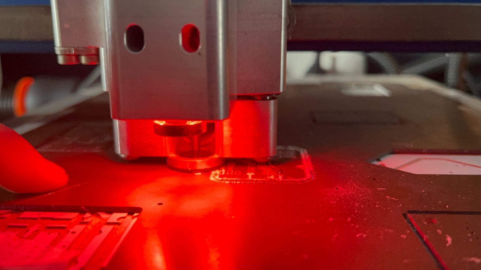
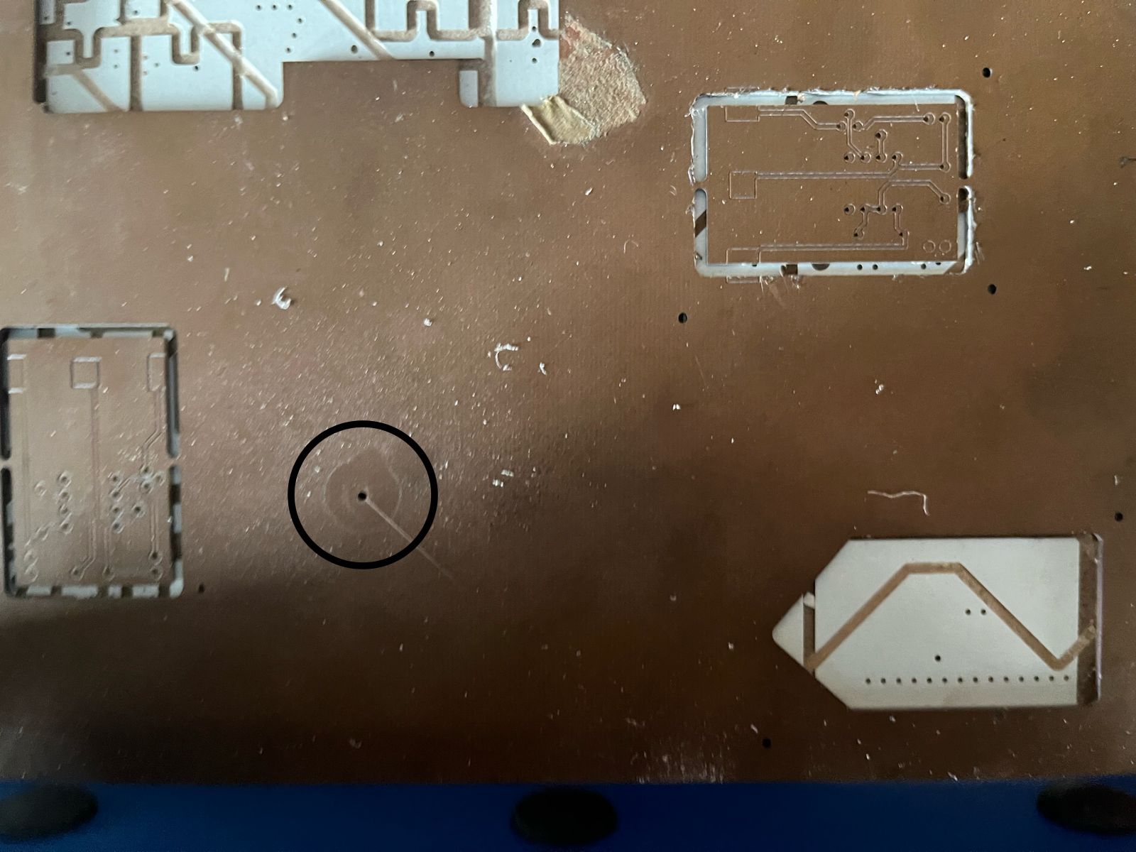
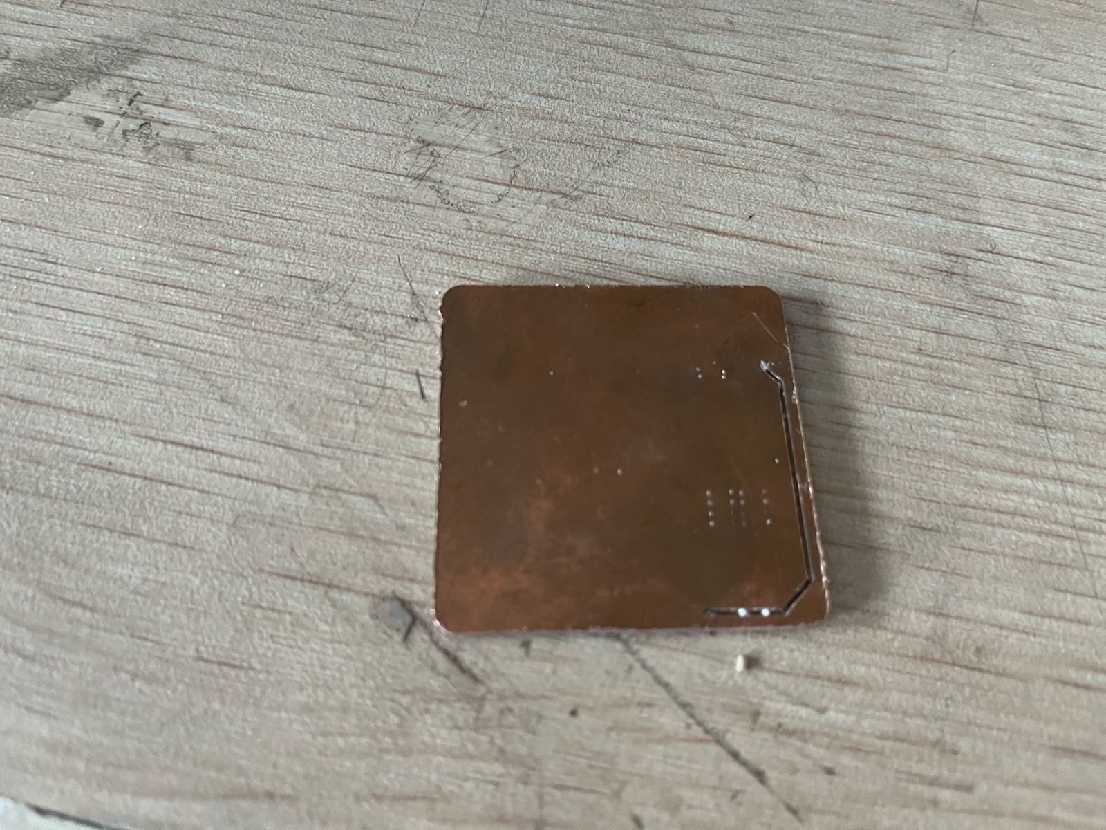
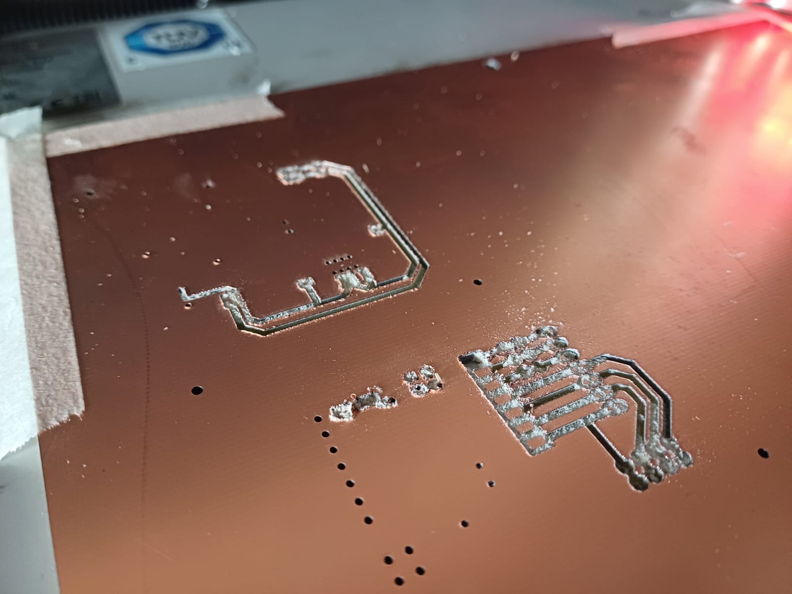
While we were doing this step,the universal cut went through and through created a big hole of the line and the tool also broke. we started figuring out why this happened as it created a hole in a line at the start on 1 vertical line but then till the end it was proper. We thought we used the wrong tool but that was not the case and then we realised that the copper plate was too old it was last used 8 months back and we did on the same sheet and did not change the sheet.
The 2 steps which did not happen
Step 11d: Reference hole
Tool: Spiral Drill 2mmm
This is reference hole drilling to start the boundary cut
Step 11e : Boundary cut
Tool: Contour router 2mmm
This step is the last one to actually cut the outer boundary of the PCB
Draft 2
Now we did a 2nd try of the same file, we changed the old copper plate and inserted a new copper plate.
We repeated the same steps
The first 2 steps were perfect again while doing universal cut it made a through to through hole in a straight line and then it stopped cutting and the sheet was plain.
After removing the tool we saw that the tool was broken again
Now again we were trying to debug the error but everything was perfect and now we thought the error was in the file .
Dradt 3
This time we thought that the error is in the file so we used Jesal sir's file
This time also the first 2 steps were perfect but again during universal cut the tool was about to break and we couldn't afford to loose 1 more tool so we paused the file in between
Draft 4
Now we realised that the error is in some settings as sir's file was already tested a year back when he was doing the fab academy so the problem is not the file now. We opened last years jesal sir's screen recording and checked what was the settings we have done earlier and we changed it accordingly.
We made some changes in the settings they were-

2. In drilling layers keep everything to automatically assigned.
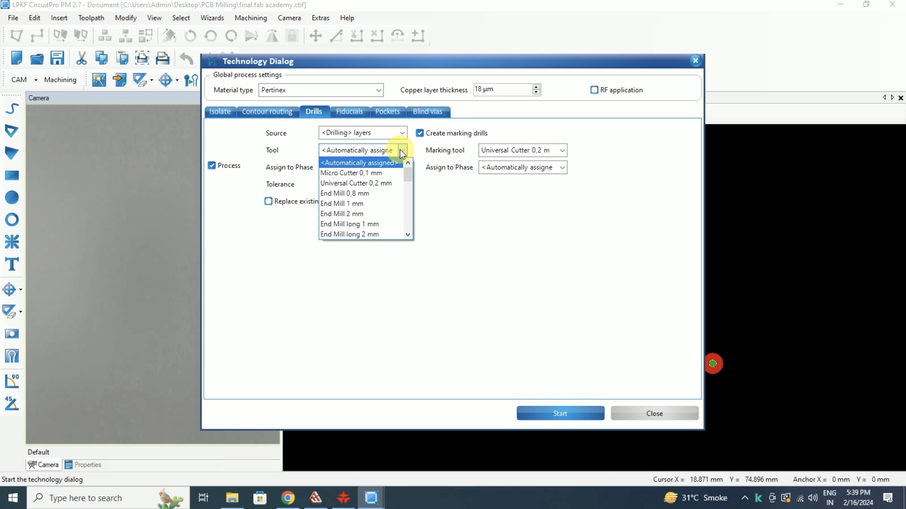
3. In fiducials also make everything to automaticaaly assigned.
4. Don't change anything in pocket, earlier also we did not change.
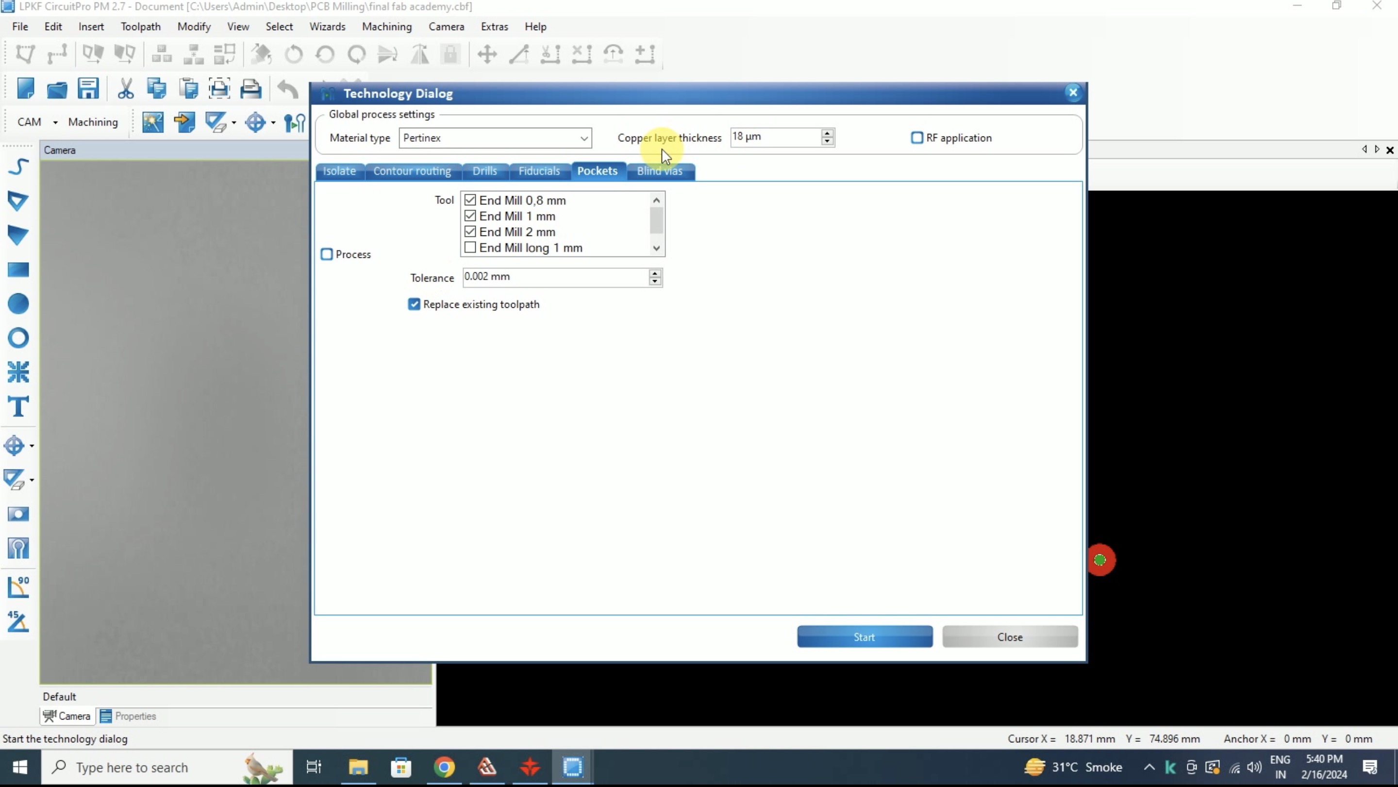
5. Initially in the materials it was FR4 earlier and now we changed it to pertinex.
After all this changes we again inserted and started doing the same steps but again the same error was occuring and we stopped doing.
Conclusion
After all this we found that our camera sensor is not working and we need to manually set the Z-Axis everytime we do. So for timming we shifted to SRM 20 and if time permits we will again try this machine.
SRM 20
We had srm 20 too in our lab so we tried that machine too
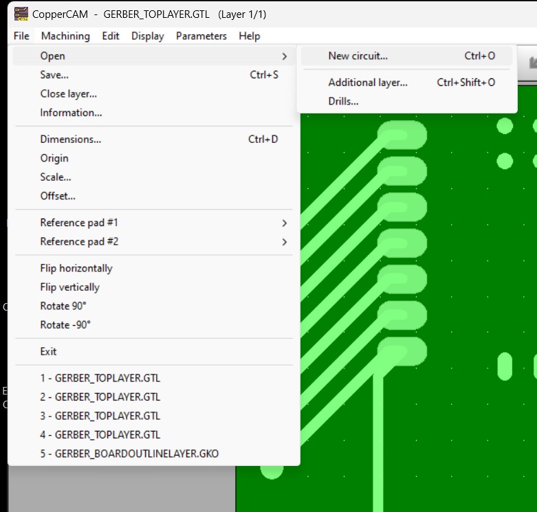
For SRM 20 the software required is copper cam.
Our E44 Protomat machine error was not sorted and we started lagging the work of week 4, So for that reason I did electronic design week's pcb first and then did Quentorres board. I documented copper cam software and milling process for week 8- electronic design.
Exploration for using SRM 20 machine
As our machine was not working and it started working during week 8- electronic design, so first we did all trials, learned milling, multimeter, soldering on our personal pcb board and then once that assignment was done we did week 4- electronic prodution.
So everything is documented in detail on Week 8
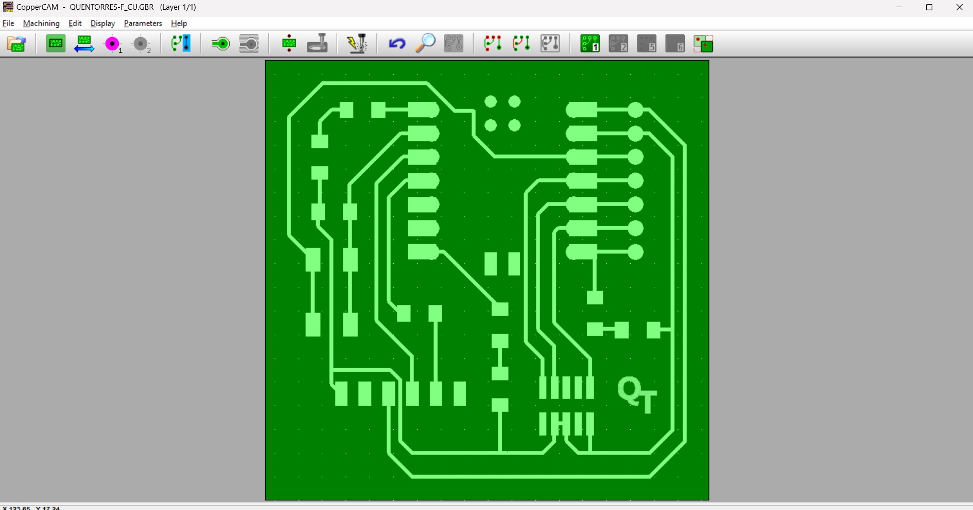
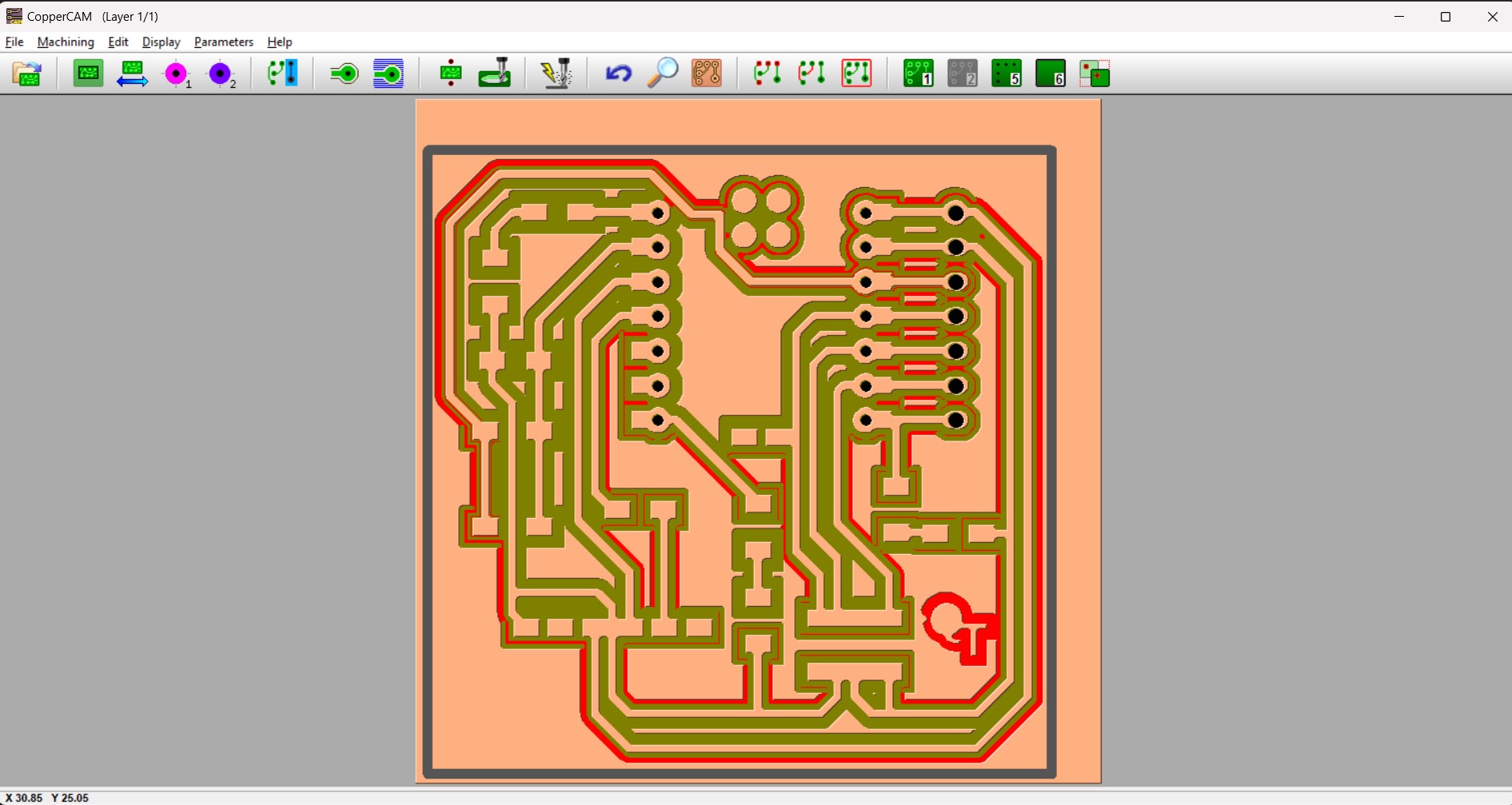
Once the PCB file is ready I started with milling the PCB. Here are the steps for the same
At the start import your file:
File > Open > Select your file > Top layer
Board outline layer will be selected later, as we did not have bottom layer and bottom solder mask layer we didn't selected that

This is how it looks after importing the file
Now repeat the same steps and add drill layer and this is how it will come after importing
Now we need to allign the drill layer with top layer
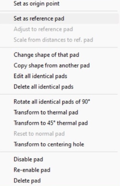
Select drill layer (5) > Right click > set as origin > again right click > Set reference pad
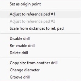
Now select drill layer:
Right click > set as origin > Again Right click > Adjust reference pad
Now repeat the same steps and select board outer layer it should automatically go in layer 6
You can see numbers from 1 and 2 they are the layers. Layer 1 and 2 are for one sided PCB, 3 and 4 are for double sided PCB ,in this machine we cannot do 2 sided pcb, the 5th one is for drilling holes and 6th one is for outer line.
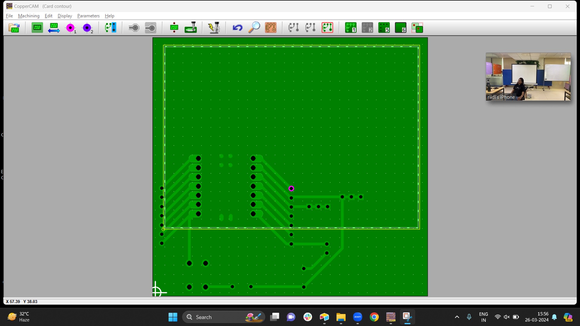
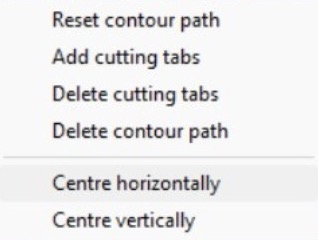
For alligning the outer box with the other layers :
Select outer layer > allign horizontally
Again Select outer layer > allign vertically
For engraving we use 0.8 conclave tool and for cutting and drilling holes we use 0.2 conclave. If we don't have any tool we can add it from tool library, every tool has a fixed parameter so whatever tool we are adding we need to add it's parameter like diameter, profile, angle and so on.
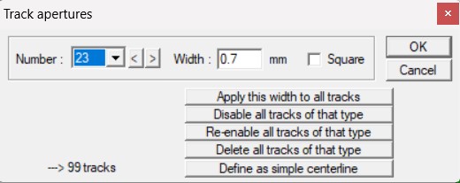
Go to track apentures and put track width as 0.7mm, this we got after a lot f try and error as shown in Week 4
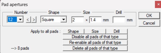
Now go to pad apentures and adjust pad width we kept it as 1.02 * 2.03
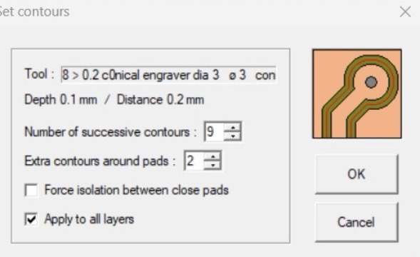
Now after preparing file go to calculate conteurs here you can see number of successive conteurs meaning how many times our tool will go on tracks and pads, set it as 2 because if it fails one time it can cut or engrave the 2nd time. Keep apply to all layers on.
This is how it looks after all the above settings is done
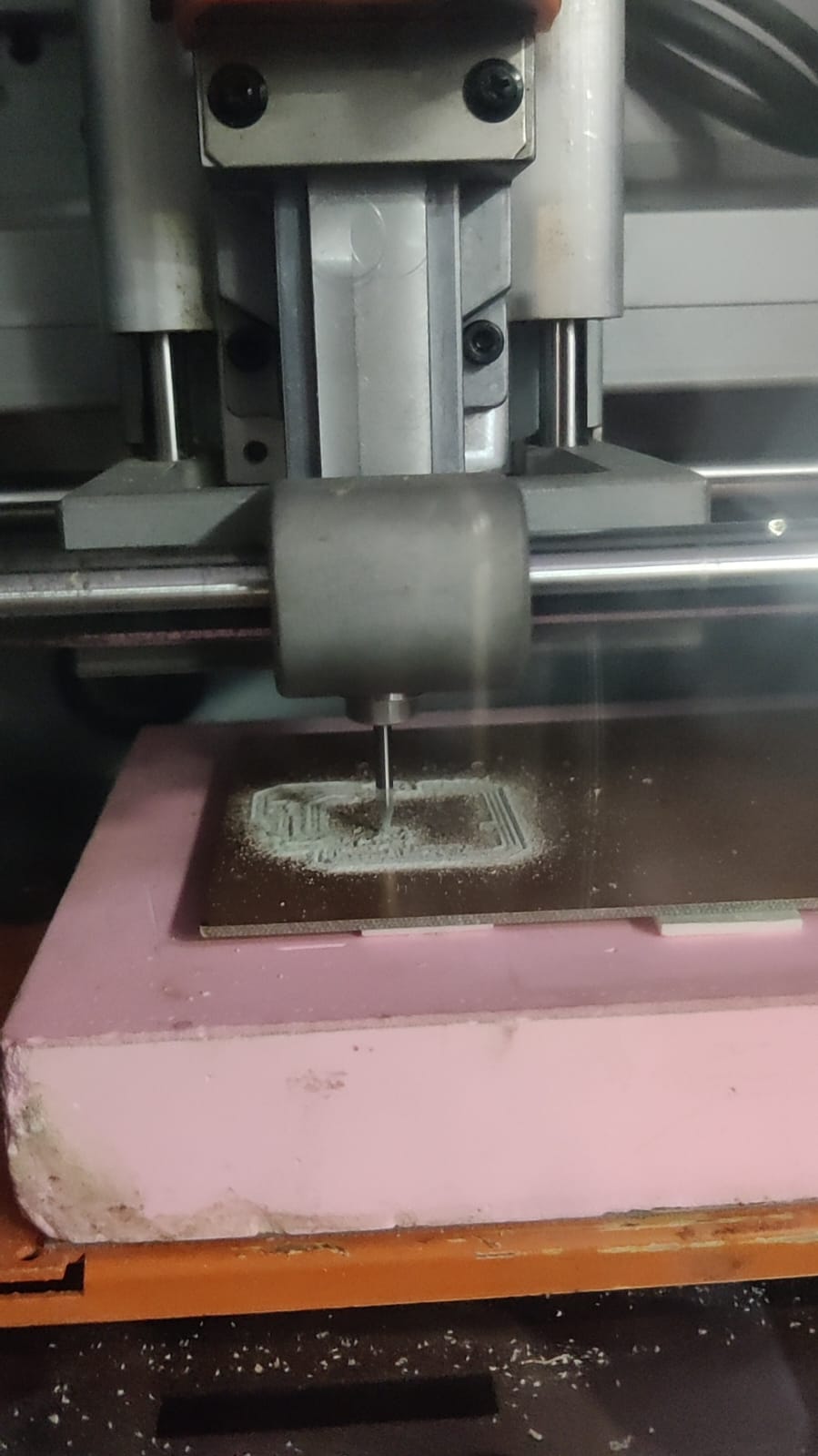
Milling
Important Tip
Srm Machine will not work if the door is kept open, after every step you do make sure the door is closed.
After all the setting is done now it's time for milling, take the single sided or double sided copper plate depending on what you want, I used single sided copper plate and on the back side put double tape and stick it on machine's bed.
As mentioned above we use 0.8mm tool for engraving and 0.2mm tool for drilling and cutting, we normally do engraving first, followed by drilling and then cutting the outer box because if we do cutting first there is a chance that the board can shake as engraving is very detailed and takes the maximum time as compared to all the 3 operations.
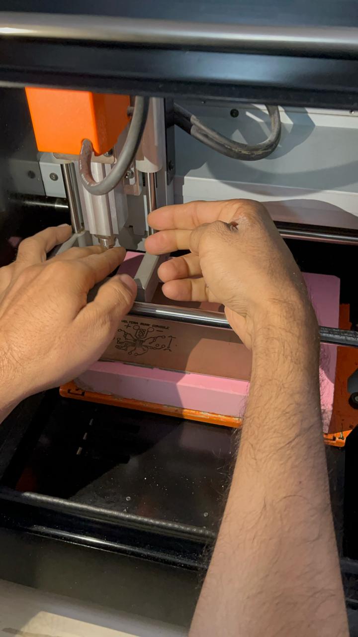
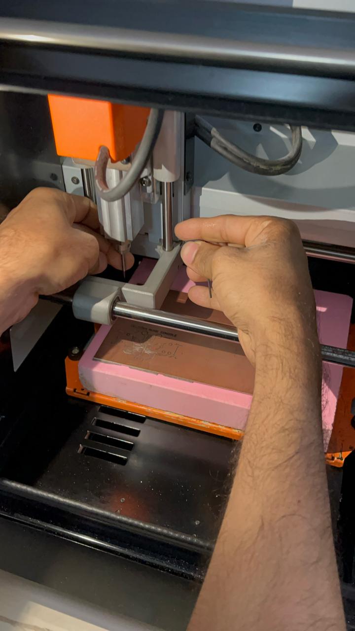
Now fit the tool, I did 0.8mm first, there is an allen key which I used for loosening the path where the tool fits, just move the screw with the allen key and once it's loosens up fit the tool inside and tight it again.
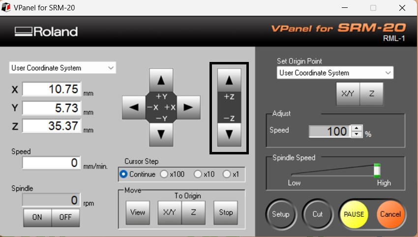
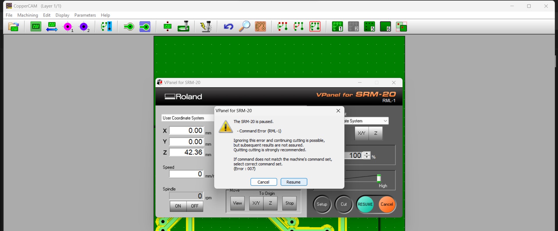
Close the door and open V-pannel software which is the software for controlling X,Y and Z axis. As I mentioned above we normally do engraving first so open output window and select engraving.
Once that is done now set X and Y axis in V-Pannel software.
We need to set Z-axis manually, we can do it in V-pannel software by pressing downward arrow as shown in the image, but here it is risky if you press the arrow and the bit touches the copper plate directly and in speed there is a high chances of drill getting break.
How to do it?
In v-pannel press z-axis downward key slowly and don't touch it to the copper plate keep it 4-5mm above of the copper plate, then open the door of the machine and loosen the screw little bit the tool will fall on the copper plate and you will be able to here a tool touching sound and then again tighten the tool.
After closing the door the Z-axis is set automatically.
Now start engraving, when you press start, machine starts after that a precaution message pop up will come that whether you want to continue milling it press continue and it will start engraving.
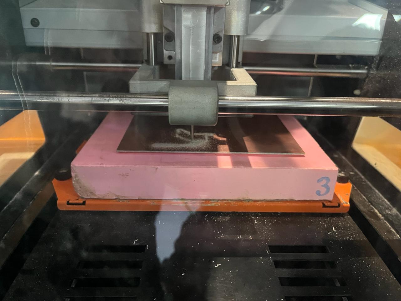
After engraving is done open the door you will see a lot of copper dust as the copper plate is engraved use vaccum dust cleaner to remove the dust before doing anything else then change the tool and put 0.2mm tool with the same process as explained above, this tool will do drilling and cutting both.
Don't change X,Y and Z origin it remains same you don't need to set it again. Again open the output window and select drilling now and start drilling holes, once that is done repeat the same steps and do cutting.
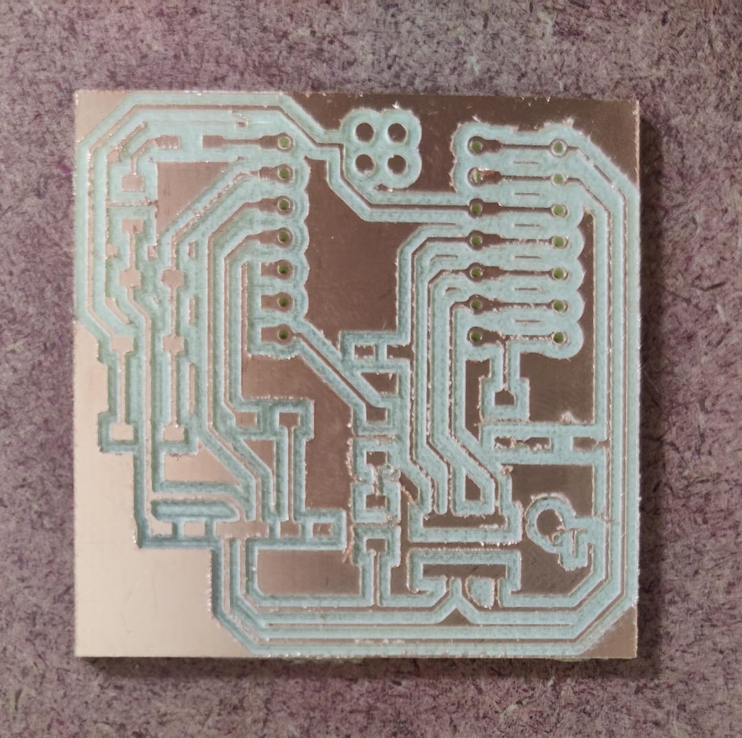
Again use vaccum to clean the dust and move the bed ahead and remove the board. You are done!
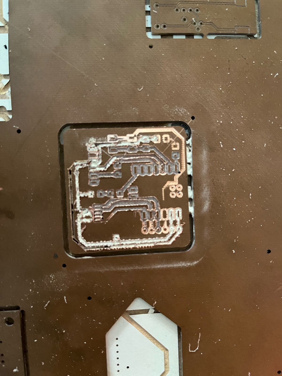
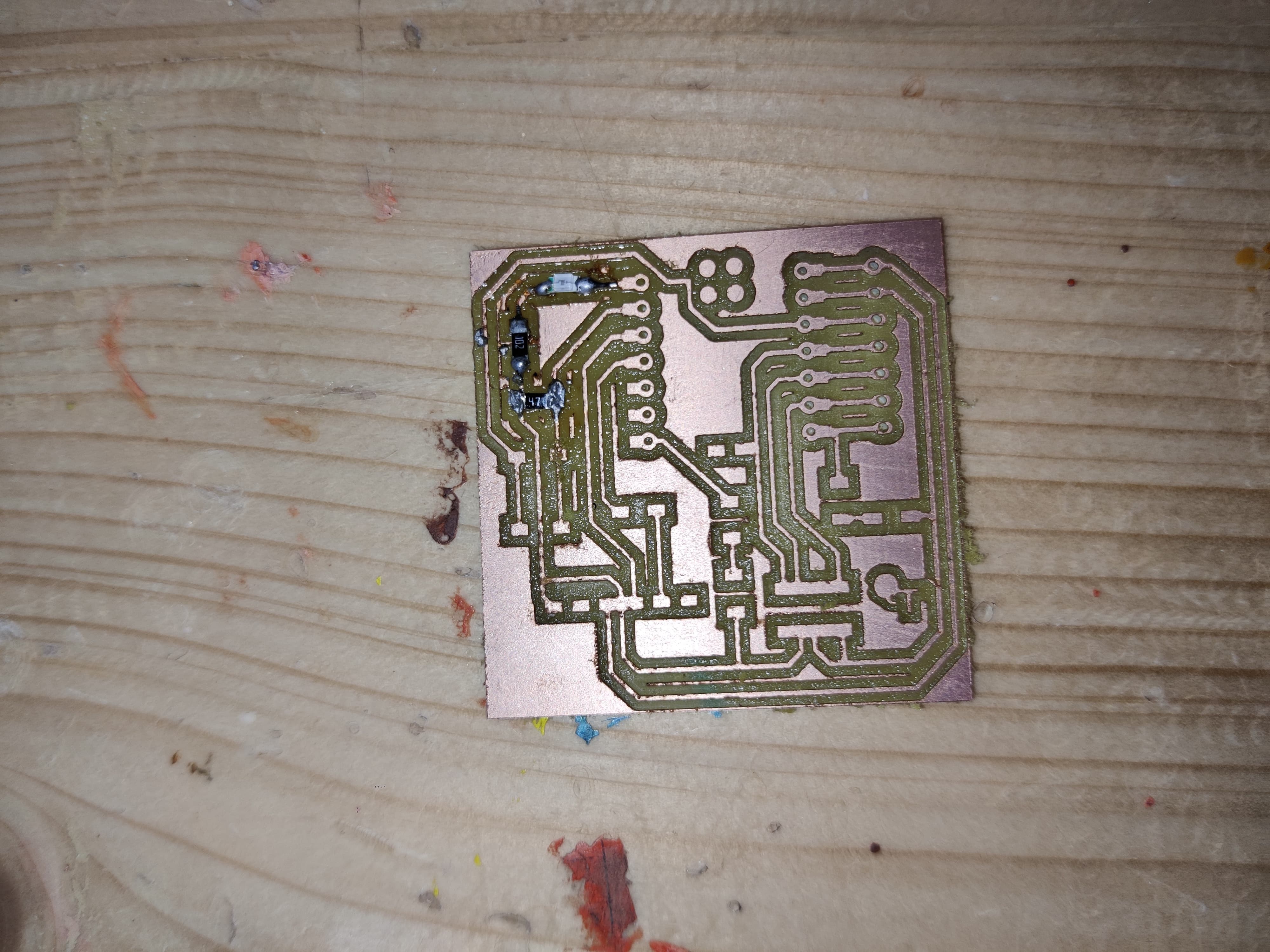
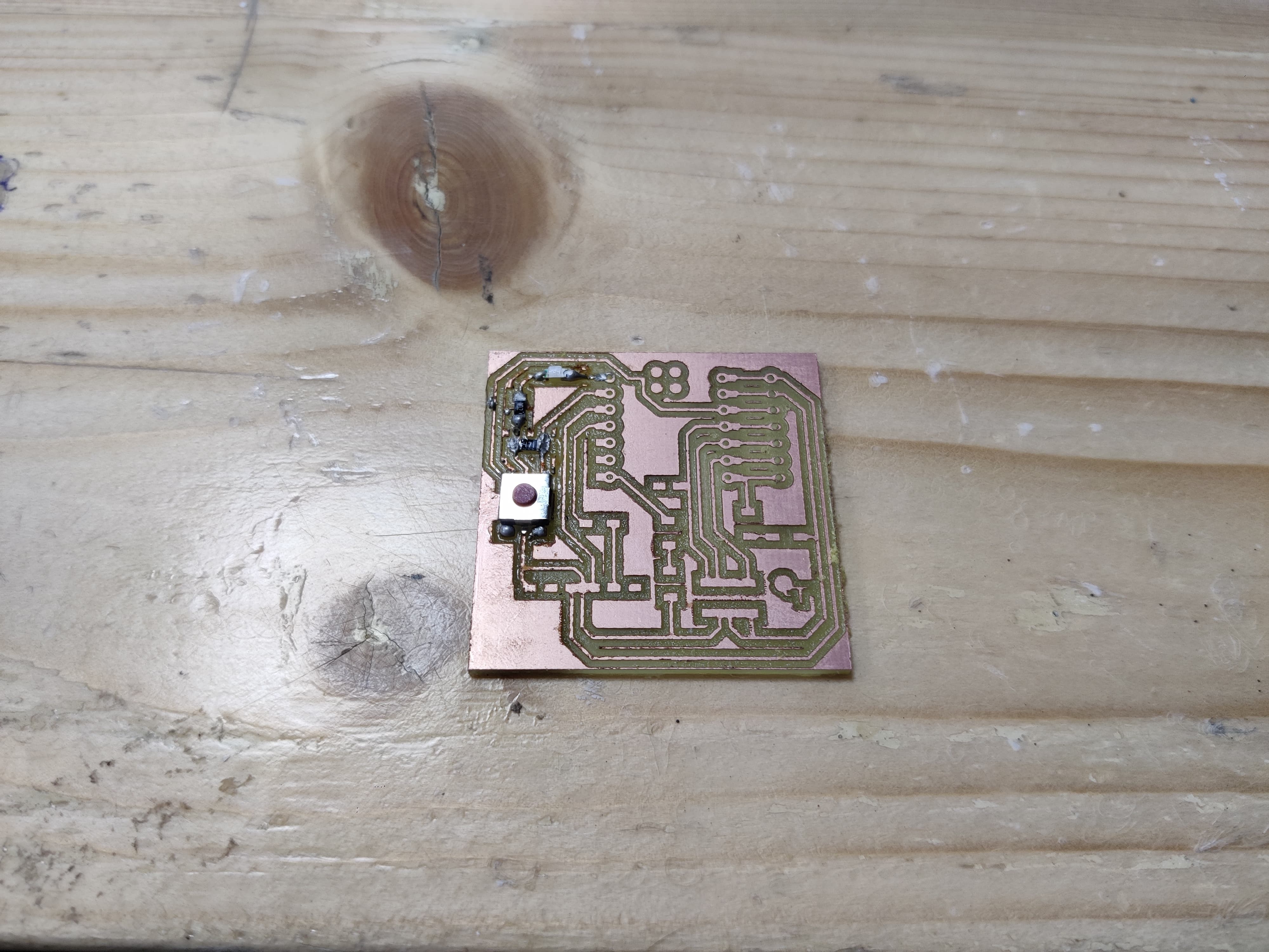
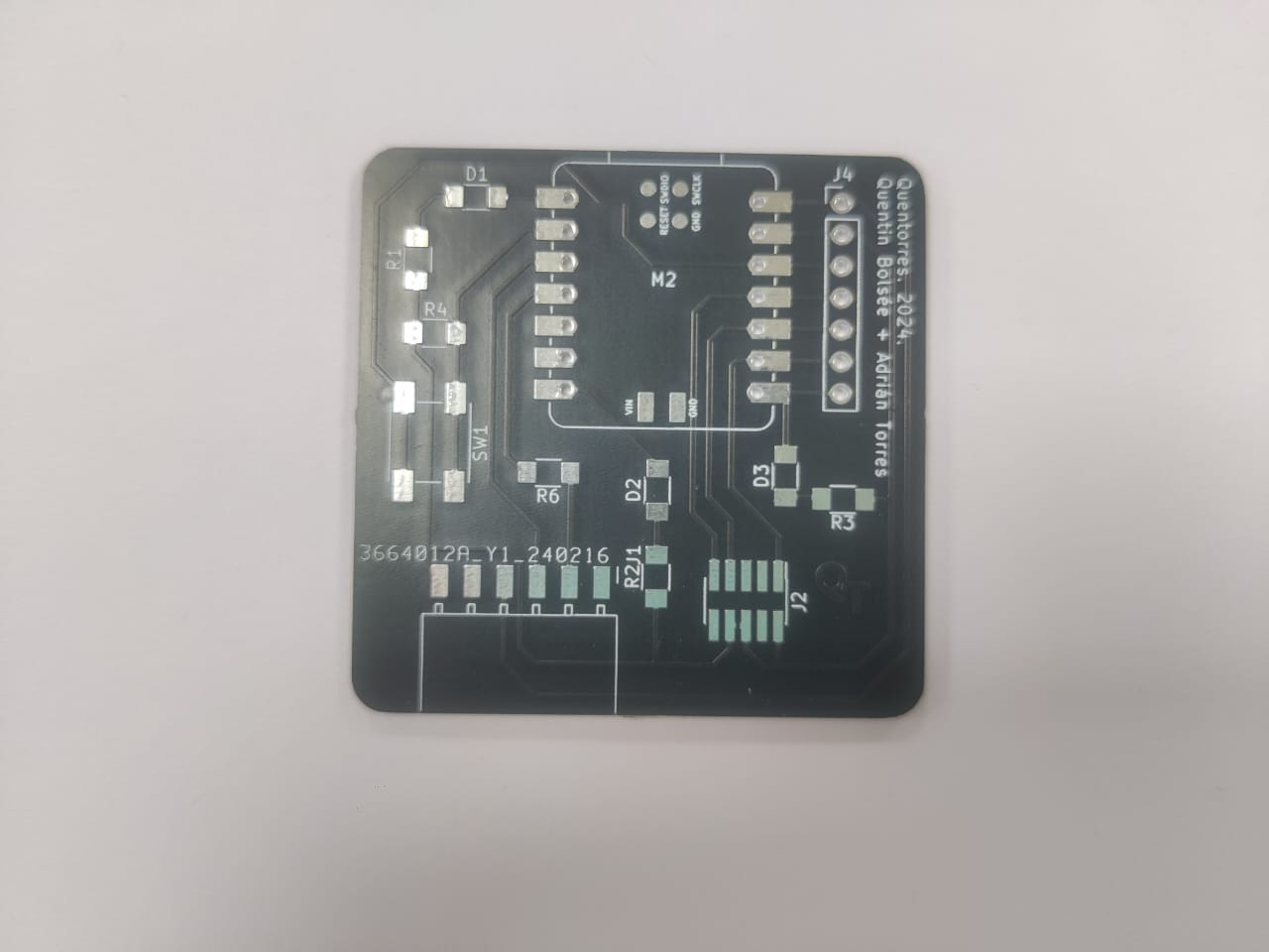
Pcb after milling
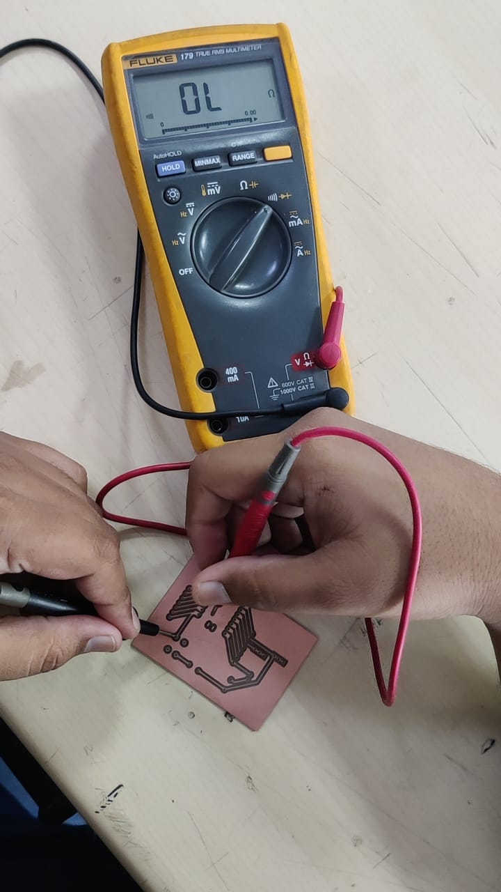
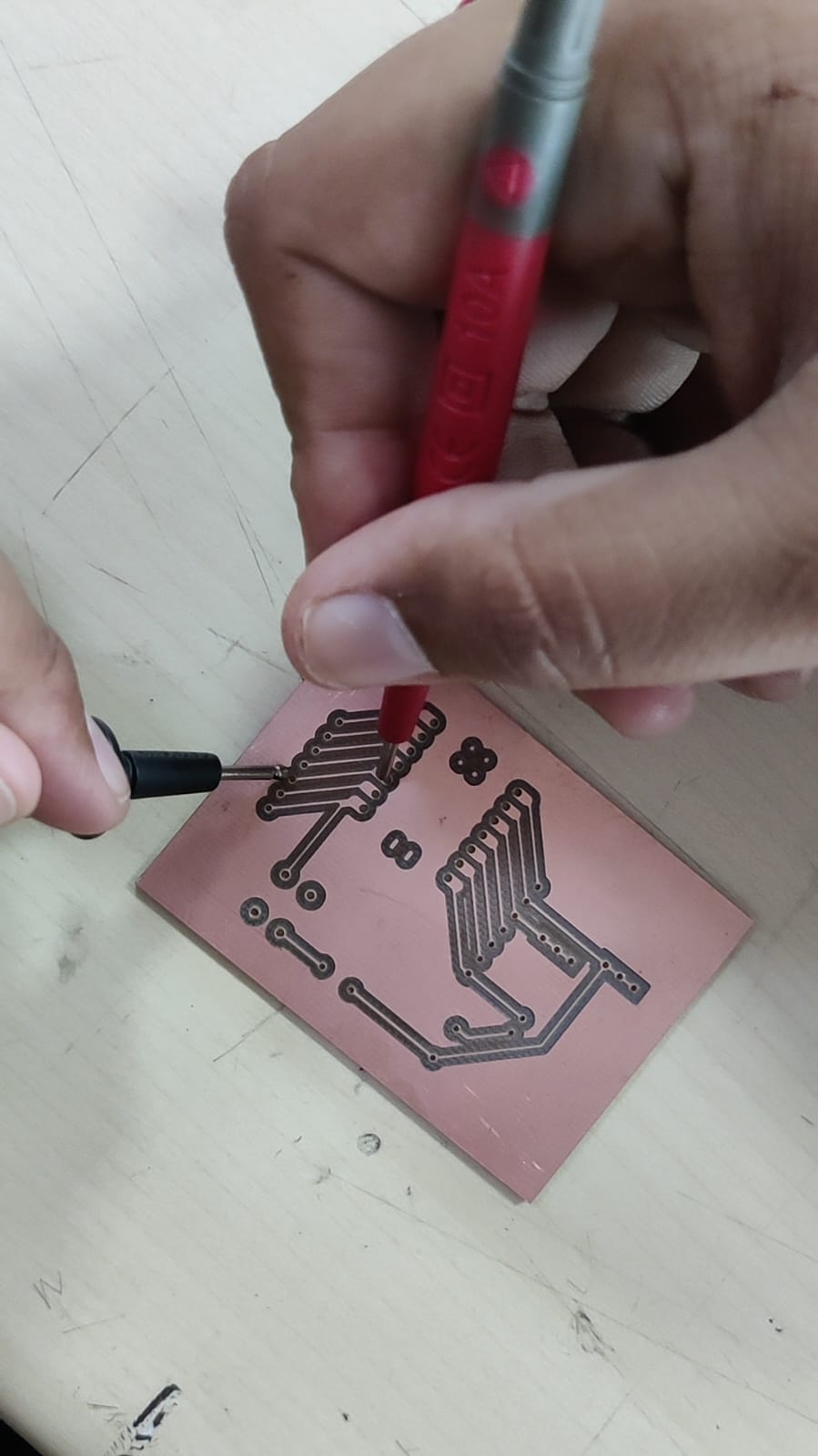
Multimeter Testing
As mentioned above we did multimeter testing forweek 8 first so i have documented that here.
Before starting the soldering we did multimeter testing, There are 2 pen like structures called test probes which you need to keep on 2 connection and it beeps so if it beeps it means it is working and if it does not beep there is some error.
To see the video of multimeter testing, click below:
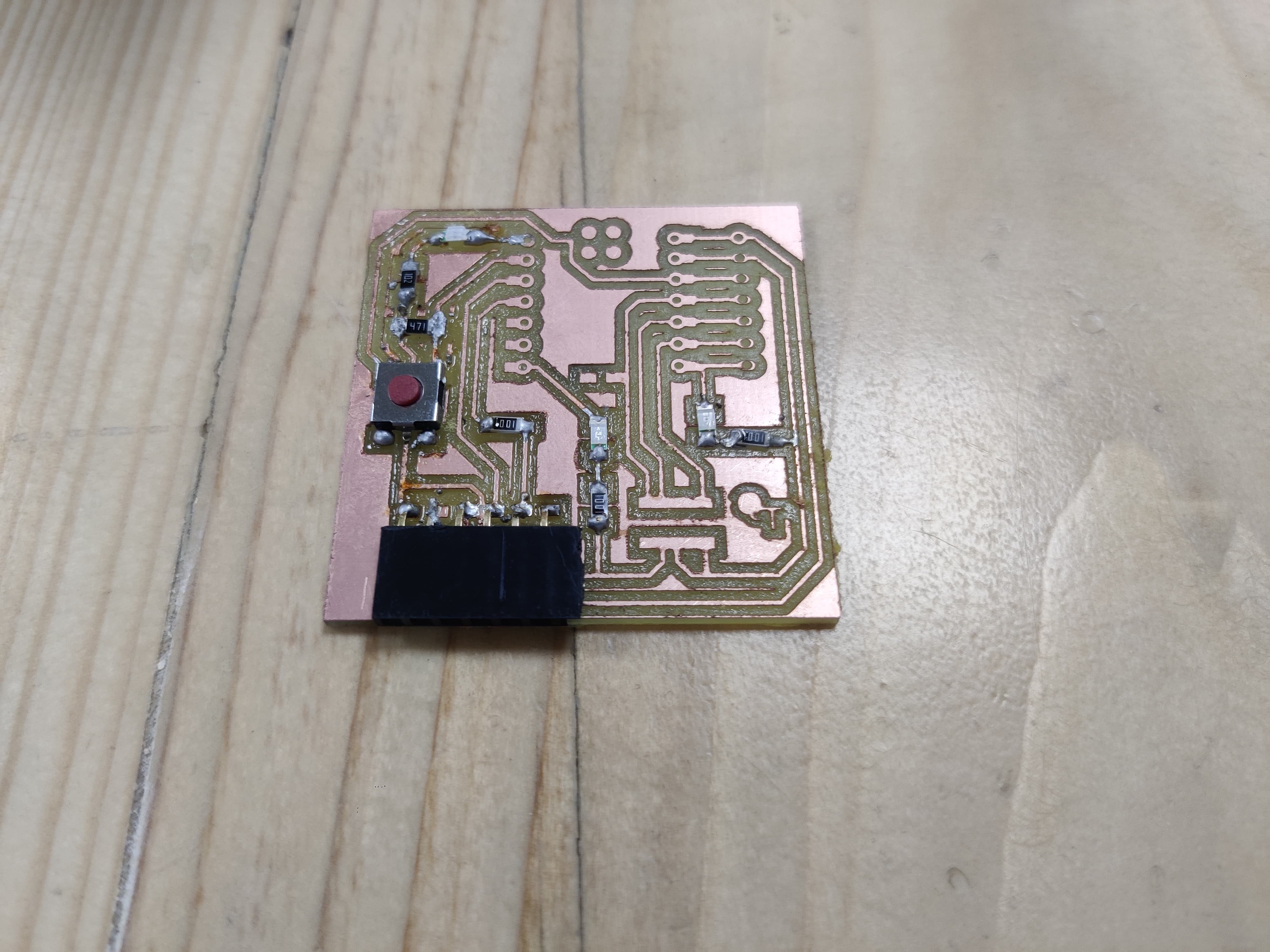
Soldering
What is soldering?
Soldering PCB, or Printed Circuit Board, involves joining electronic components to the board using solder, a low-melting-point metal alloy. This process creates secure electrical and mechanical connections between the components and the PCB substrate. It's a fundamental technique in electronics assembly, crucial for creating complex circuits in electronic devices. Soldering is done using a soldering iron or station, applying heat to melt the solder and form connections between components and the PCB.
Things require to do soldering
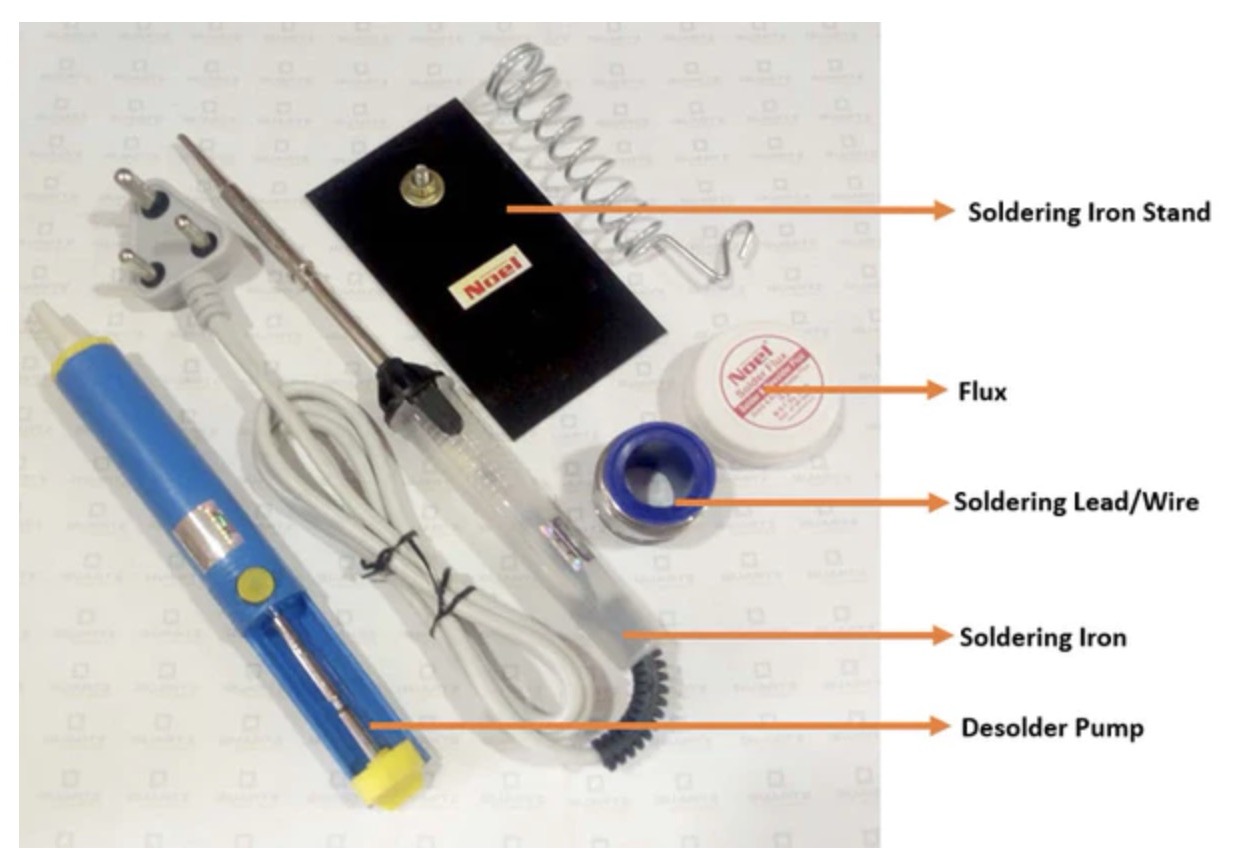
Soldering Iron:
A tool that heats up to melt solder and make connections.
Solder Wire:
A metal alloy that melts at a low temperature to create electrical connections.
Flux:
A chemical compound applied to the joint to clean and promote solder flow.
Soldering Stand:
A stand to hold the soldering iron when not in use, preventing accidents, often equipped with a magnifying glass for precision work.
Helping Hands:
Adjustable tool with clips to hold components and PCBs in place during soldering.
Desoldering Pump or Wick:
Tools to remove excess solder or correct mistakes.
Safety Gear:
Heat-resistant gloves, safety glasses, and a well-ventilated workspace to ensure safety while soldering.
How to do soldering?
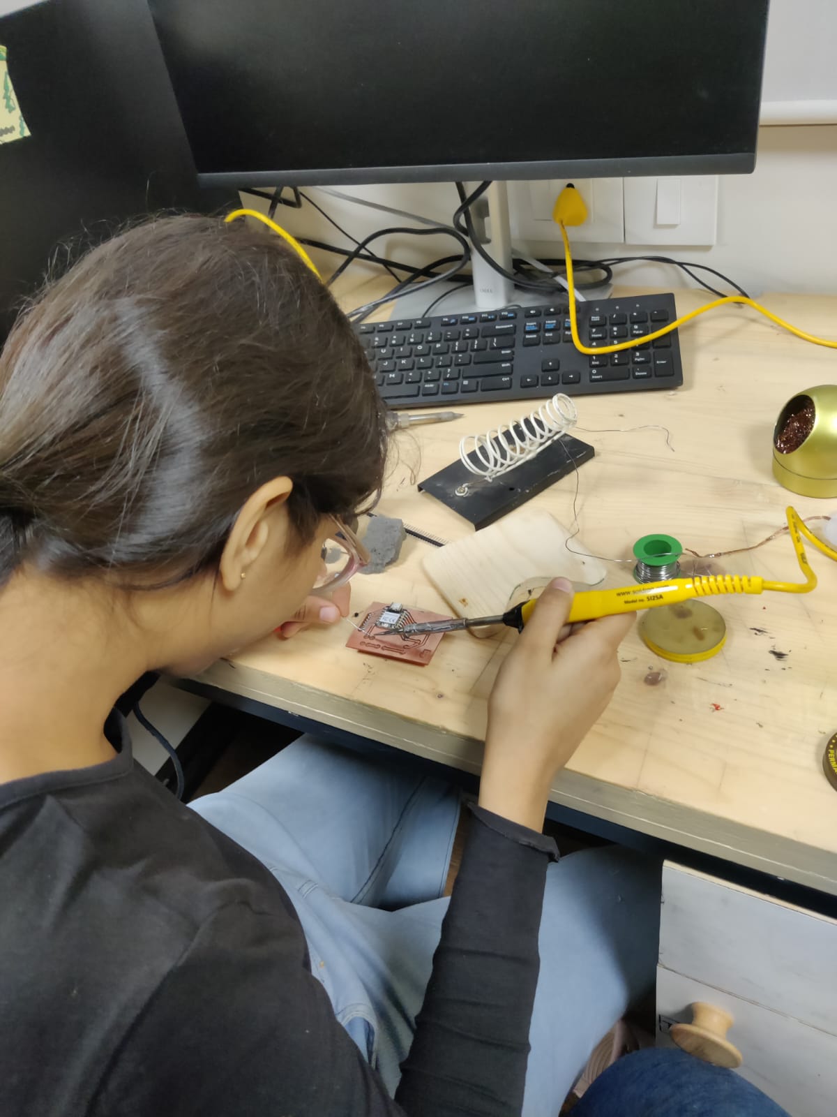
Again I soldered week 8- my personal board first so below are the photos of the same.
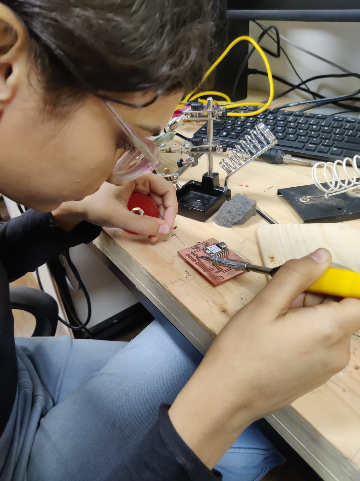
Prepare Your Work Area:
Ensure you have a clean, well-ventilated workspace. Gather all necessary tools and components.
Set Up Your Equipment:
Turn on your soldering iron and allow it to heat up to the appropriate temperature for your solder and the components you're working with. Typically, temperatures between 300°C to 400°C (572°F to 752°F) are suitable for most soldering tasks.
Tin the Soldering Iron:
Once heated, clean the tip of the soldering iron with a damp sponge or brass wire cleaner. Then, apply a small amount of solder to the tip to coat it. This process, known as tinning, helps improve heat transfer.
Prepare the Components:
Place the components you wish to solder onto the PCB. Ensure they are correctly positioned and secured.
Apply Flux:
Apply a small amount of flux to the areas where you will be soldering. Flux helps clean the surfaces and promotes solder flow, resulting in strong and reliable connections.
Heat the Joint:
With the soldering iron in one hand and the solder wire in the other, bring the tip of the iron into contact with the joint where the component meets the PCB. Hold it there for a few seconds to heat the joint evenly.
Apply Solder:
Once the joint is heated, touch the solder wire to the joint, not the soldering iron. Allow the solder to melt and flow evenly over the joint, creating a smooth and shiny connection. Ensure you use just enough solder to cover the joint without creating excess.
Remove the Solder and Iron:
Once the joint is soldered, remove the solder wire first, followed by the soldering iron. Hold the components steady until the solder cools and solidifies.
Inspect the Joint:
After soldering, visually inspect the joint to ensure it is smooth, shiny, and free from any cold solder joints or excess solder. A properly soldered joint should have a concave-shaped fillet.
Clean Up:
Clean the soldering iron tip with a damp sponge or brass wire cleaner to remove any excess solder and flux residue. Turn off the soldering iron and allow it to cool down safely.
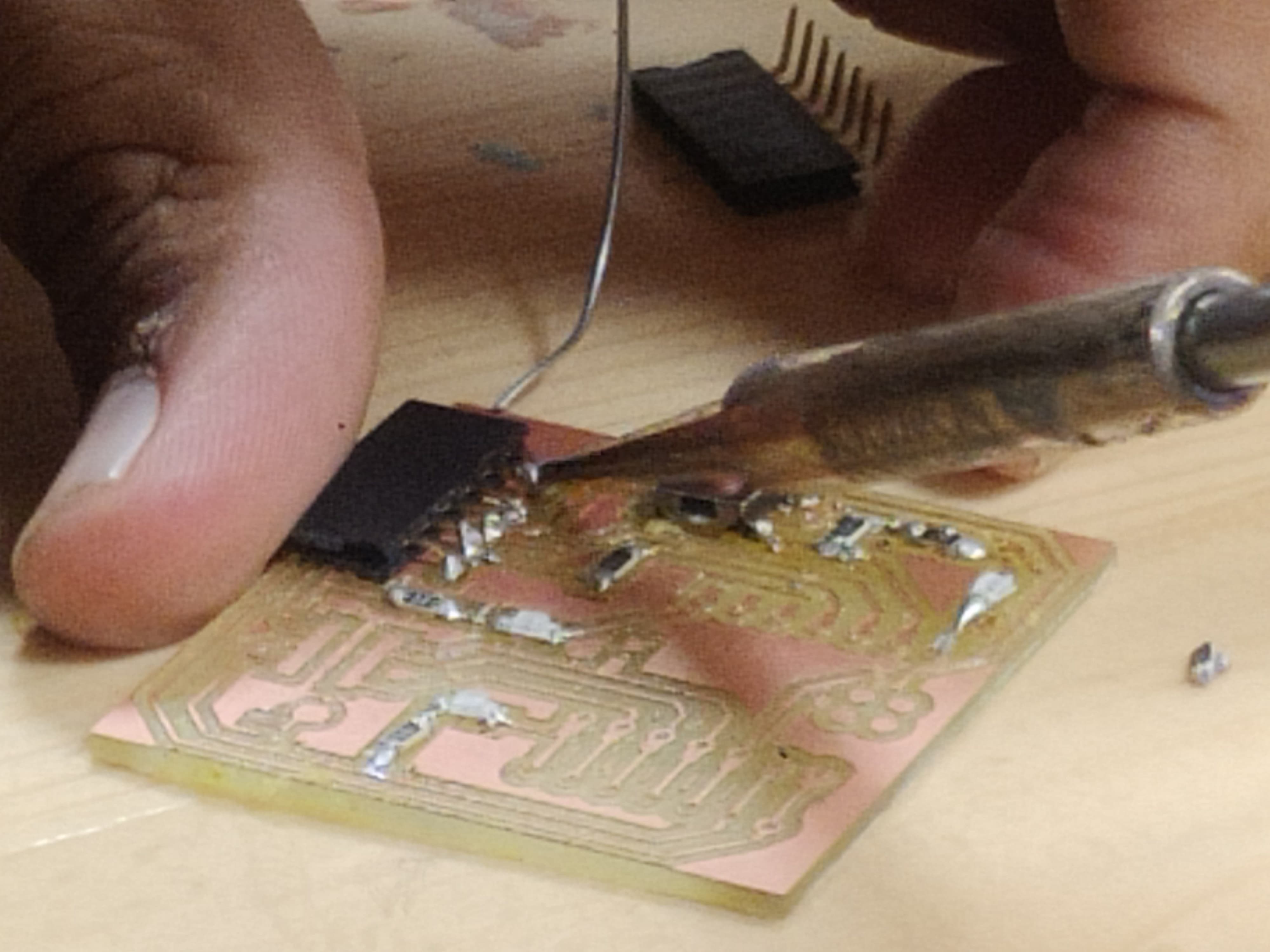
Soldering Results
Below are the images while I was doing soldering
How to desolder?
Heat Up the Solder Joint:
Using a soldering iron, heat up the solder joint you wish to desolder. Apply heat evenly to the joint for a few seconds to melt the solder.
Use Desoldering Braid or Pump:
There are two common methods for desoldering: using desoldering braid (also known as solder wick) or a desoldering pump (also known as a solder sucker).
Desoldering Braid:
Place the desoldering braid over the molten solder joint and press it down with the soldering iron. The braid will absorb the melted solder, wicking it away from the joint. Once saturated, remove the braid and trim off the used portion.
Desoldering Pump:
Position the desoldering pump over the molten solder joint and press the plunger down to create a vacuum. Release the plunger to suck up the melted solder into the pump's chamber. Repeat as necessary until the joint is clear of solder.
Remove the Component:
Once the solder has been removed from the joint, gently lift or wiggle the component to free it from the circuit board. Be careful not to damage the board or surrounding components.
Clean Up:
After desoldering, inspect the joint to ensure it is clear of solder. Use isopropyl alcohol and a clean brush or cloth to remove any flux residue from the board.
Repeat as Necessary:
Depending on the complexity of the circuit and the number of soldered joints, you may need to repeat the desoldering process for each component you wish to remove.
Inspect the Board:
After desoldering, inspect the circuit board and remaining components for any damage or defects. Repair or replace any damaged components as needed.
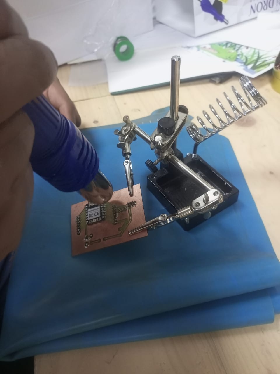
How did I desoldered my PCB ?
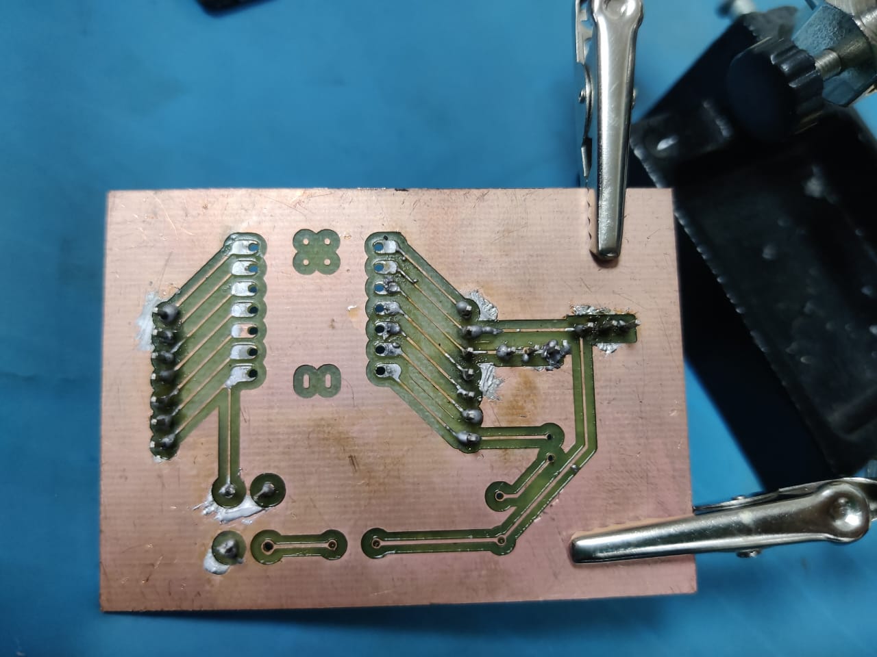
My quentorres pcb was soldered correct but in week 8 I made a mistake so I ddesoldered that pcb, so the below documentation of desoldering is for that pcb.
I tested my pcb with multimeter first and found that the right hand side line was completely shot with each other like 5V and 3V was connected with each other, gnd and d7 pin was connected with each other.
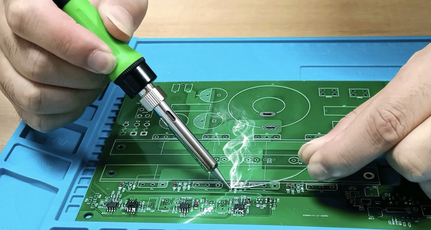
Initially while I was soldering I made an error and I used excess solder and the circuit was shot so I need to desolder it now, I tried with desoldering pump first but as I was doing that I realised that the entire base is filled with copper and now I need to use hot air pump to de solder it.
Be very careful while using hot air pump it's very hot, the ideal temperature we need is 300 to 400 degree celciusm, always have silicon mat below as the entire area gets hot. Use twisser to hold the component and put the pcb on the stand, start the gun and start melting the soldered copper once it is melted pick it up, do not touch the pcb with hands as it is very hot use twisers for the same.
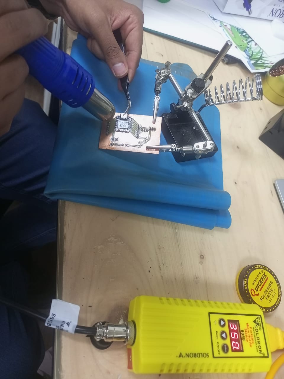
After Desoldering
After I desoldered I found the error that there was an entire copper layer down and even on one side of the pcb so now I need to clean that first with the help of soldering iron and copper wick.
I cleaned the entire copper plate and RP2040 and used it again.
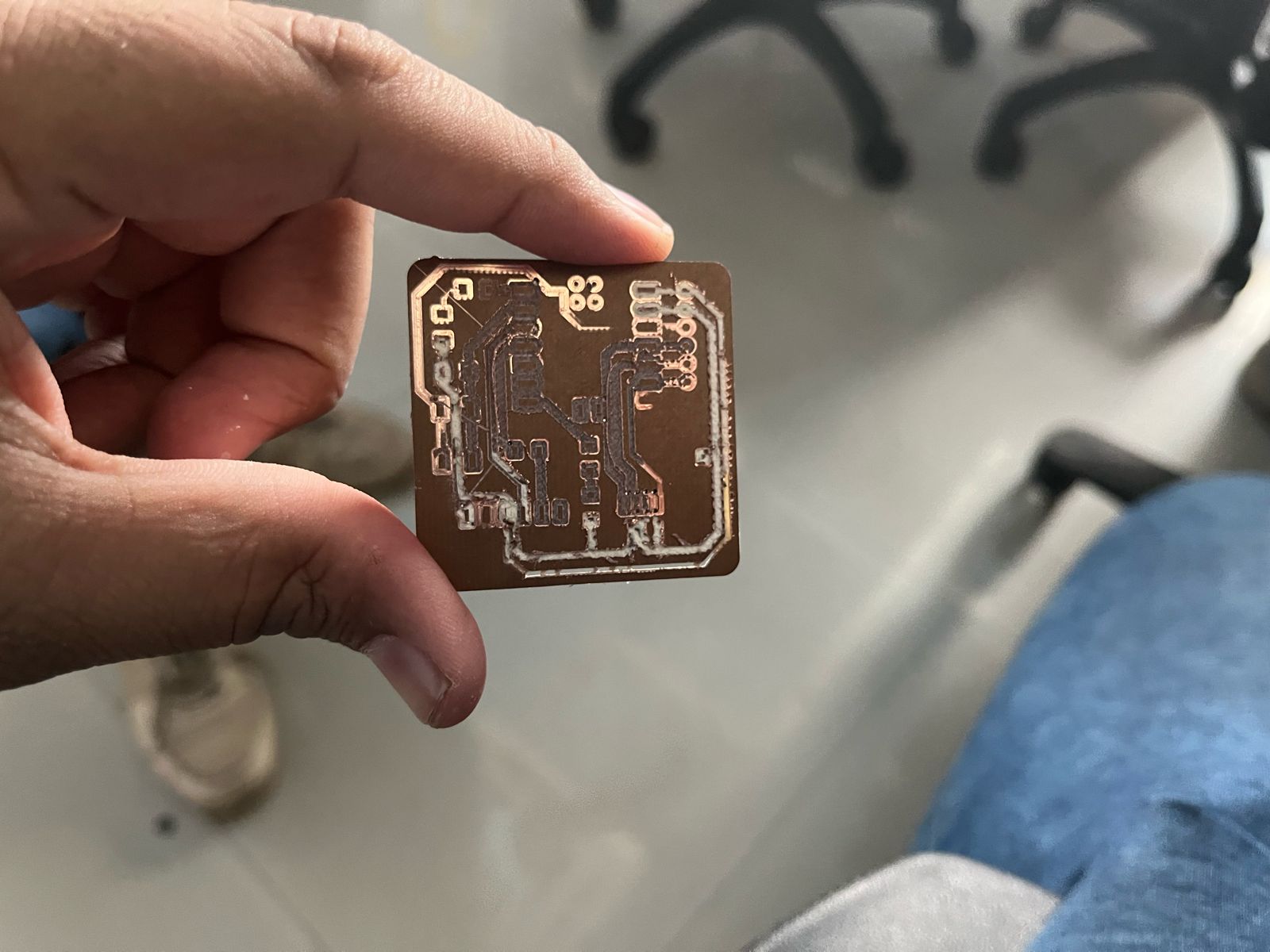
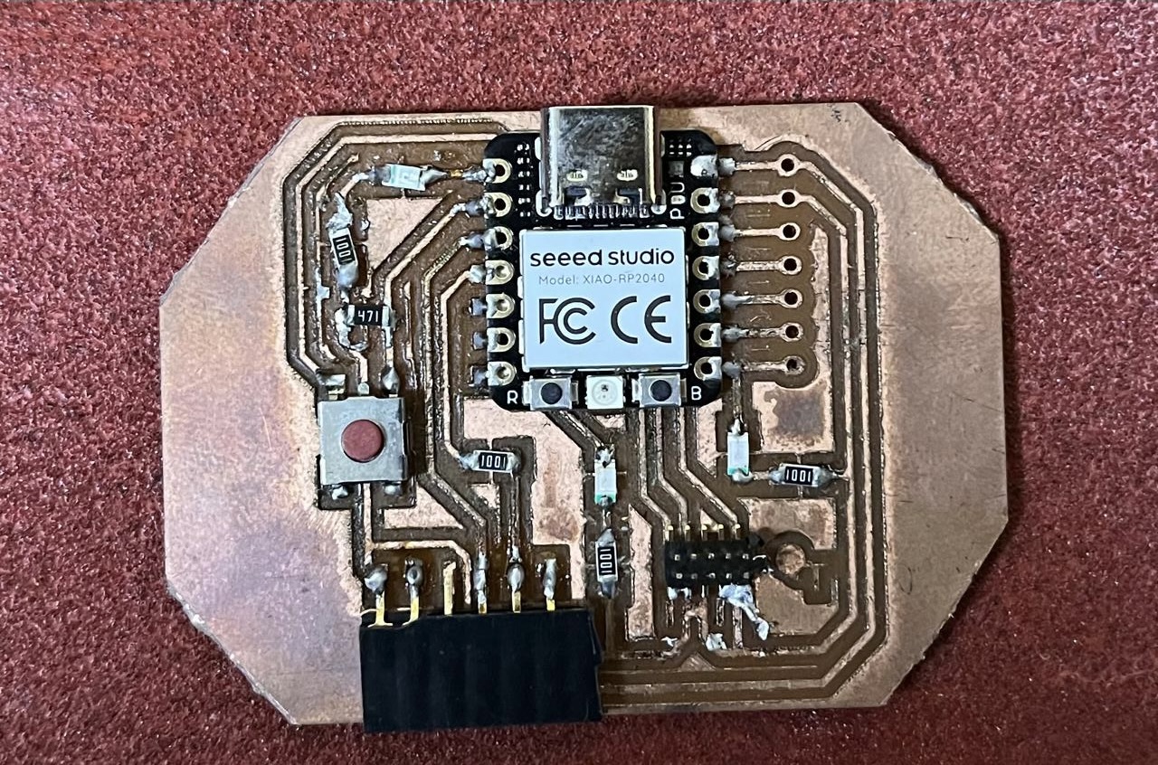
Remilled PCB
After soldering my pcb it was not working and it was difficult to desolder it as all the smd components on it was also getting desoldered, so I remilled the pcb. Steps of remilling pcb remains same as mentioned above, here are some glimpses of the same.
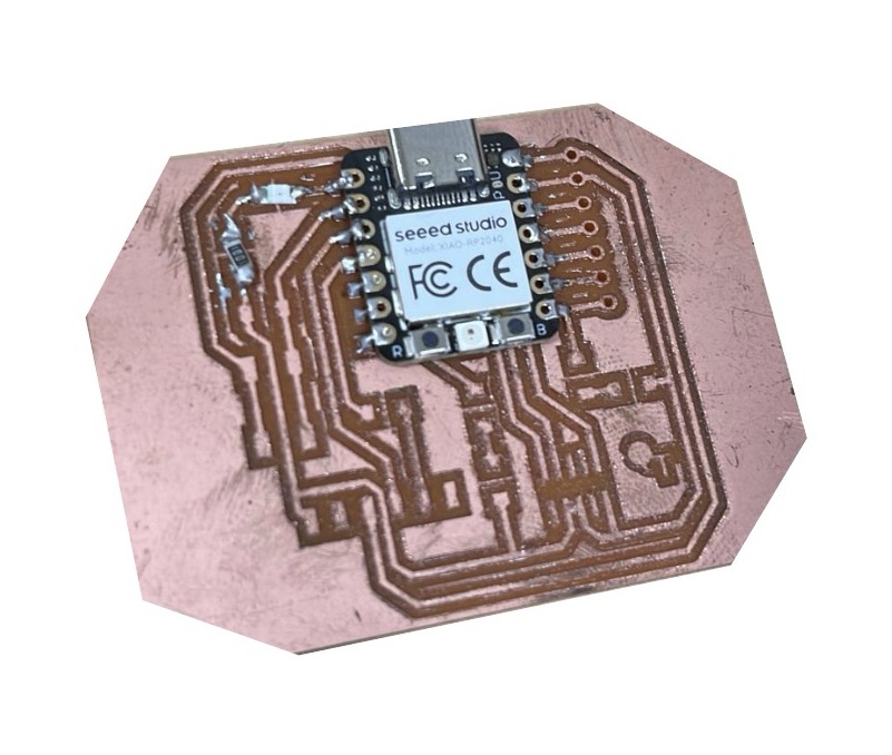
Heroshot
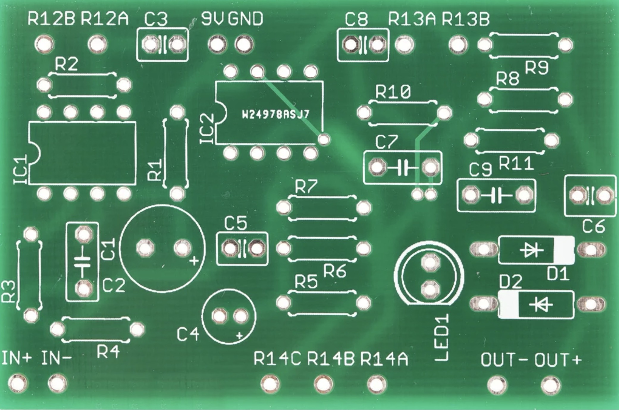
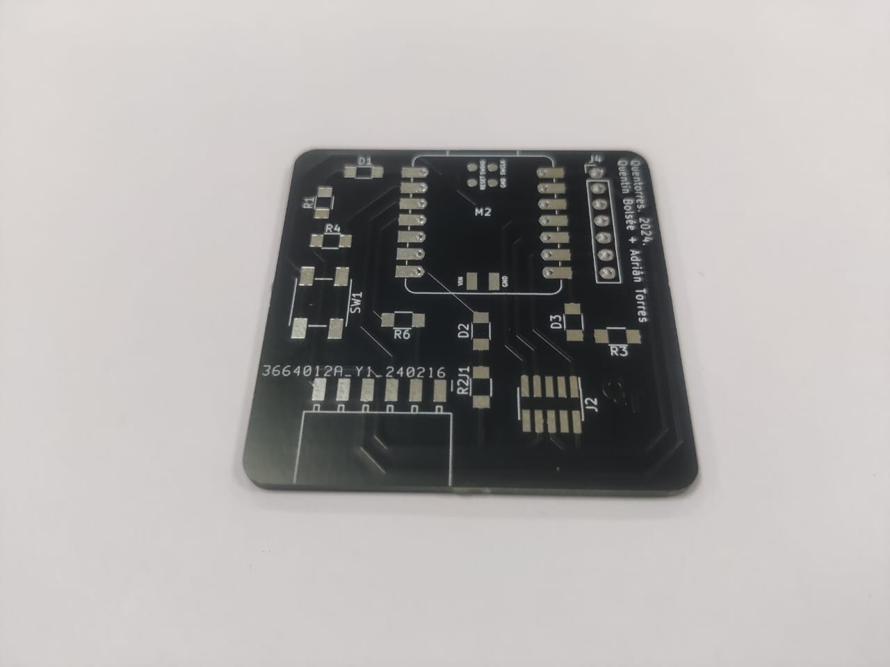
This is how my new pcb looks
Coding
// Define the pin numbers for the LEDs
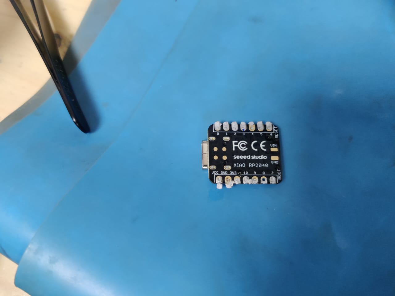
const int ledPin1 = D0; // LED on D0
const int ledPin2 = D6; // LED on D6
const int ledPin3 = D7; // LED on D7
void setup() {
// Initialize the LED pins as outputs
pinMode(ledPin1, OUTPUT);
pinMode(ledPin2, OUTPUT);
pinMode(ledPin3, OUTPUT);
}
void loop() {
// Turn on all LEDs
digitalWrite(ledPin1, HIGH);
digitalWrite(ledPin2, HIGH);
digitalWrite(ledPin3, HIGH);
// Wait for a second
delay(1000);
// Turn off all LEDs
digitalWrite(ledPin1, LOW);
digitalWrite(ledPin2, LOW);
digitalWrite(ledPin3, LOW);
// Wait for a second
delay(1000);
}
The above code controls three LEDs connected to pins D0, D6, and D7 of a microcontroller. In the setup() function, it initializes these pins as outputs. In the loop() function, it turns on all three LEDs for one second, then turns them off for one second, continuously blinking the LEDs on and off at one-second intervals.
Heroshot
Group Work
Half Group work is uploaded on Siddhart's Page and other half is below.
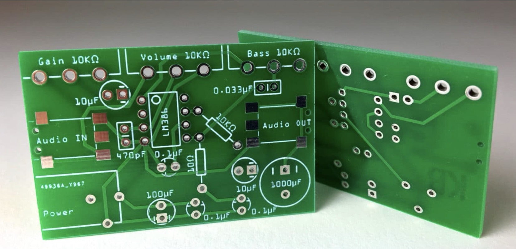
TASK 1- Ordering from JLCPCB
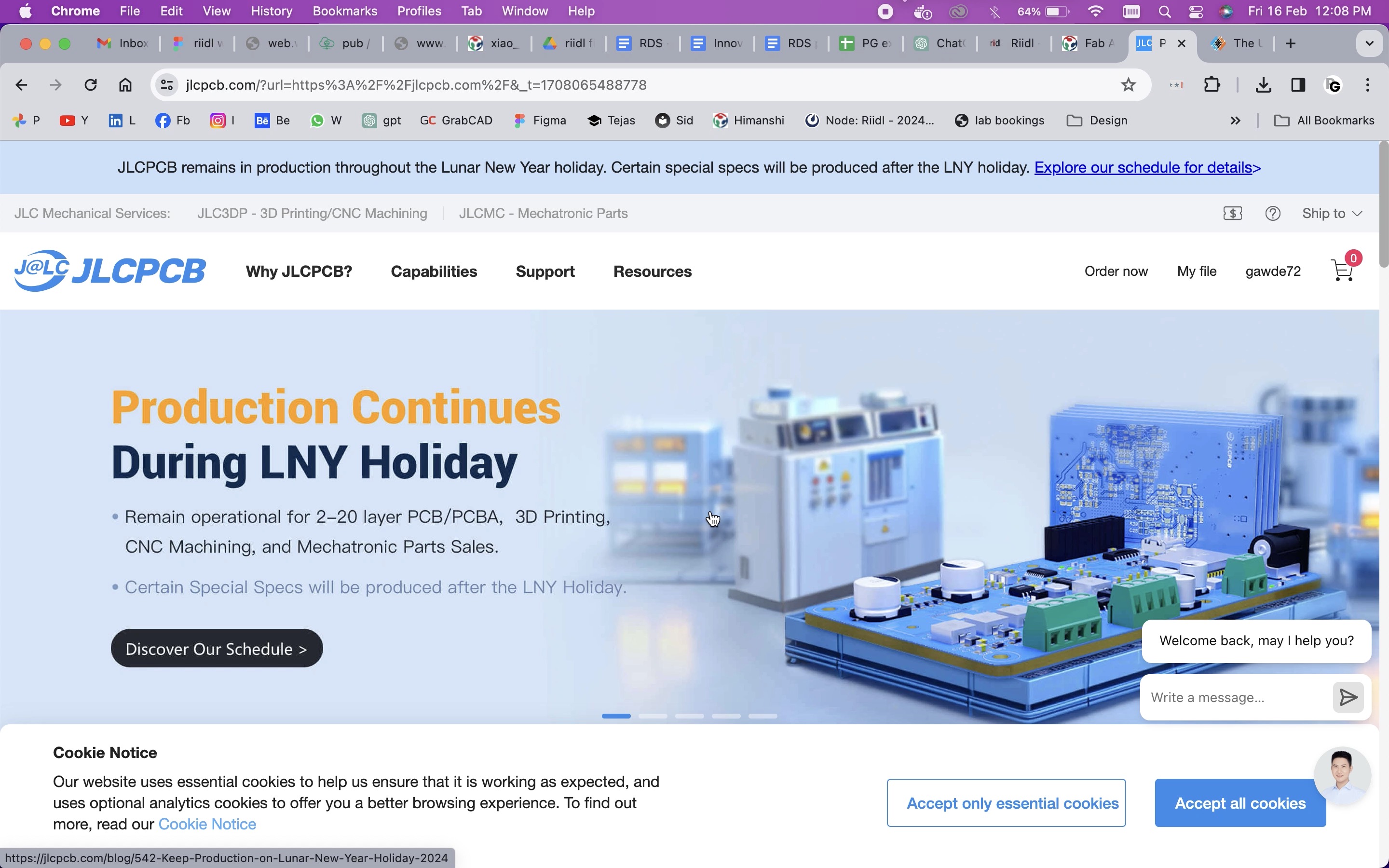
In our group it is me, Siddhart, Tejas and of course our mentors Jesal sir and Pranav sir. We ordered PCB'S from JLCPCB and here is the entire process of the same. Below is the basic interface of JLCPCB website
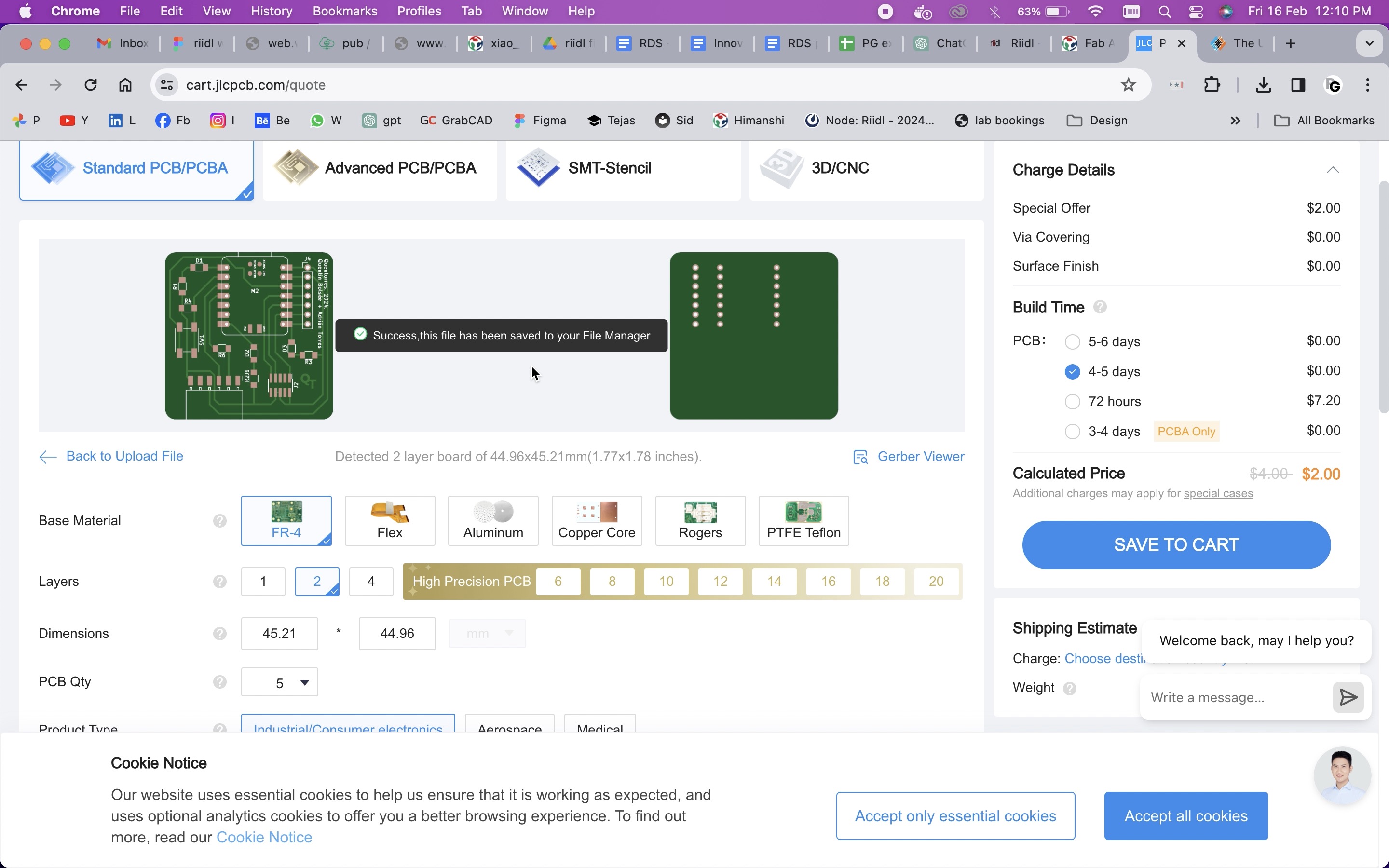
We went on order now on right hand side, here we can see standard PCB/ PCBA, Advanced PCB/PCBA, SMT- stencil and 3D CNC and we added a gerber file, after adding the file it identifies the file automatically and it si showing the front side and back side.
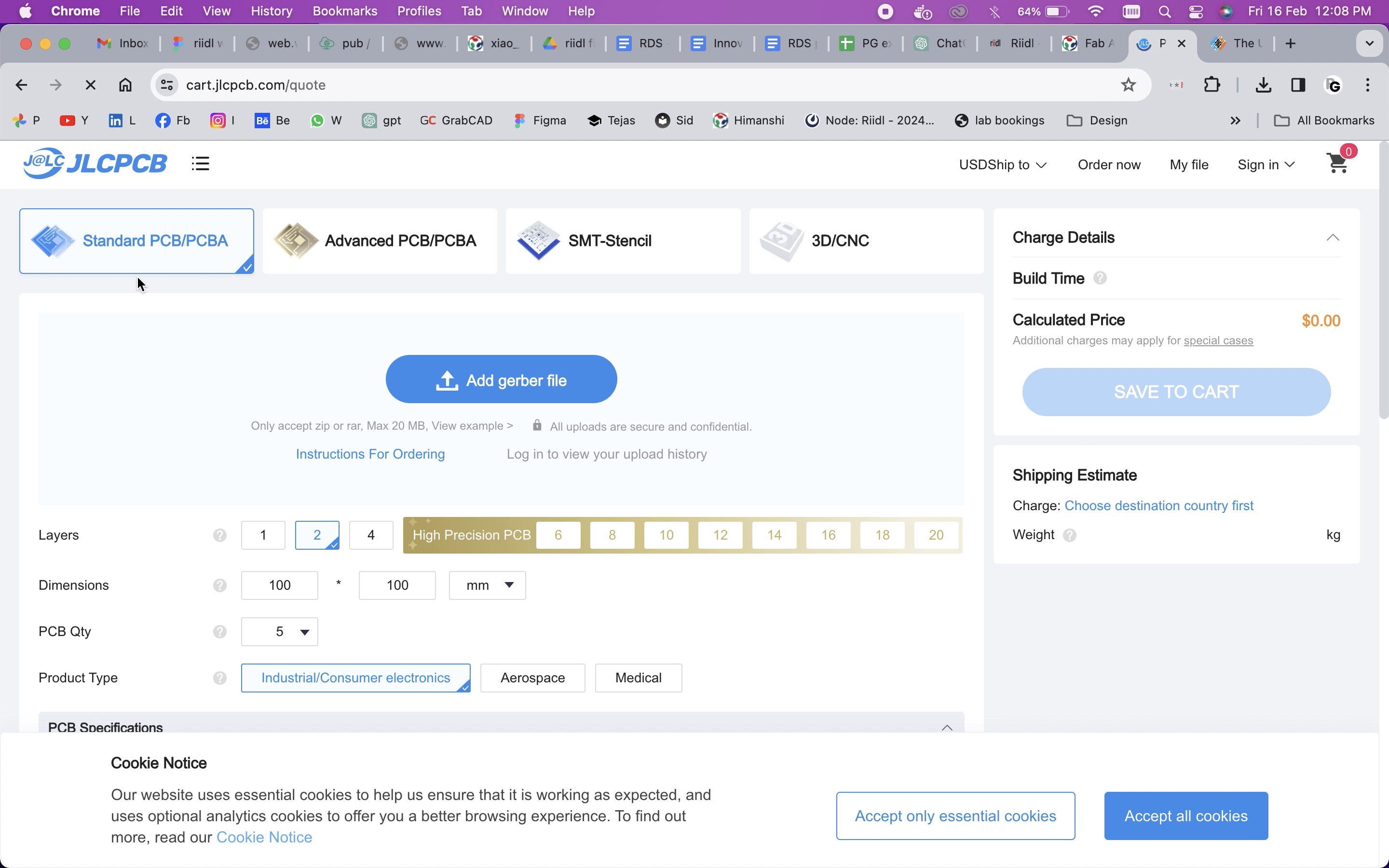
Select base material we selected FR4 i.e our normal copper plate.
In layers it selects automatically by identifying our file, it selected 2 as on the back side there are only holes for soldering mask for conducting.
It takes dimensions automatically as we uploaded our file.
For quantity we selected the minimum quantity that is 5 pieces.
For product type we have selected industrial/ consumer electronics
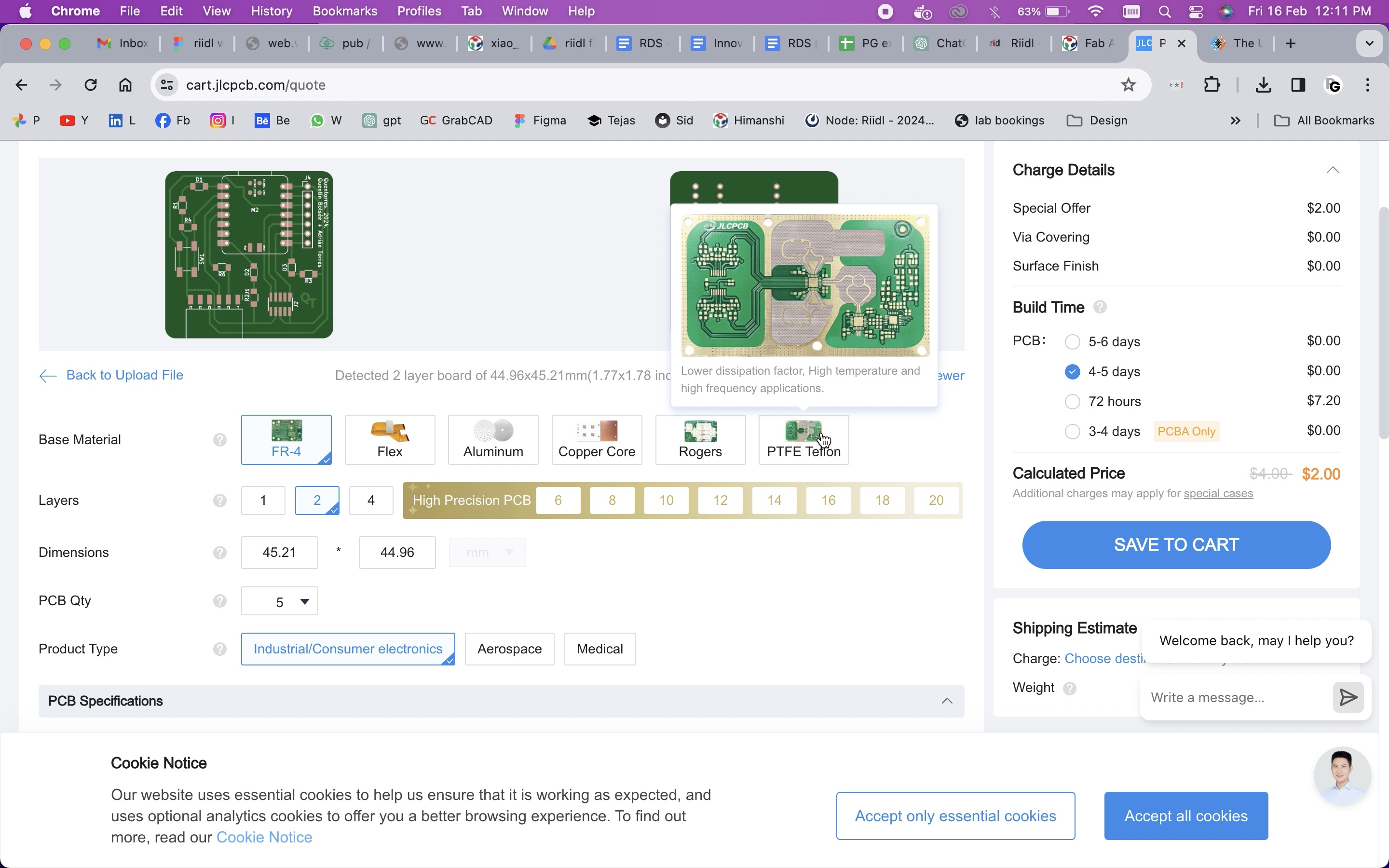
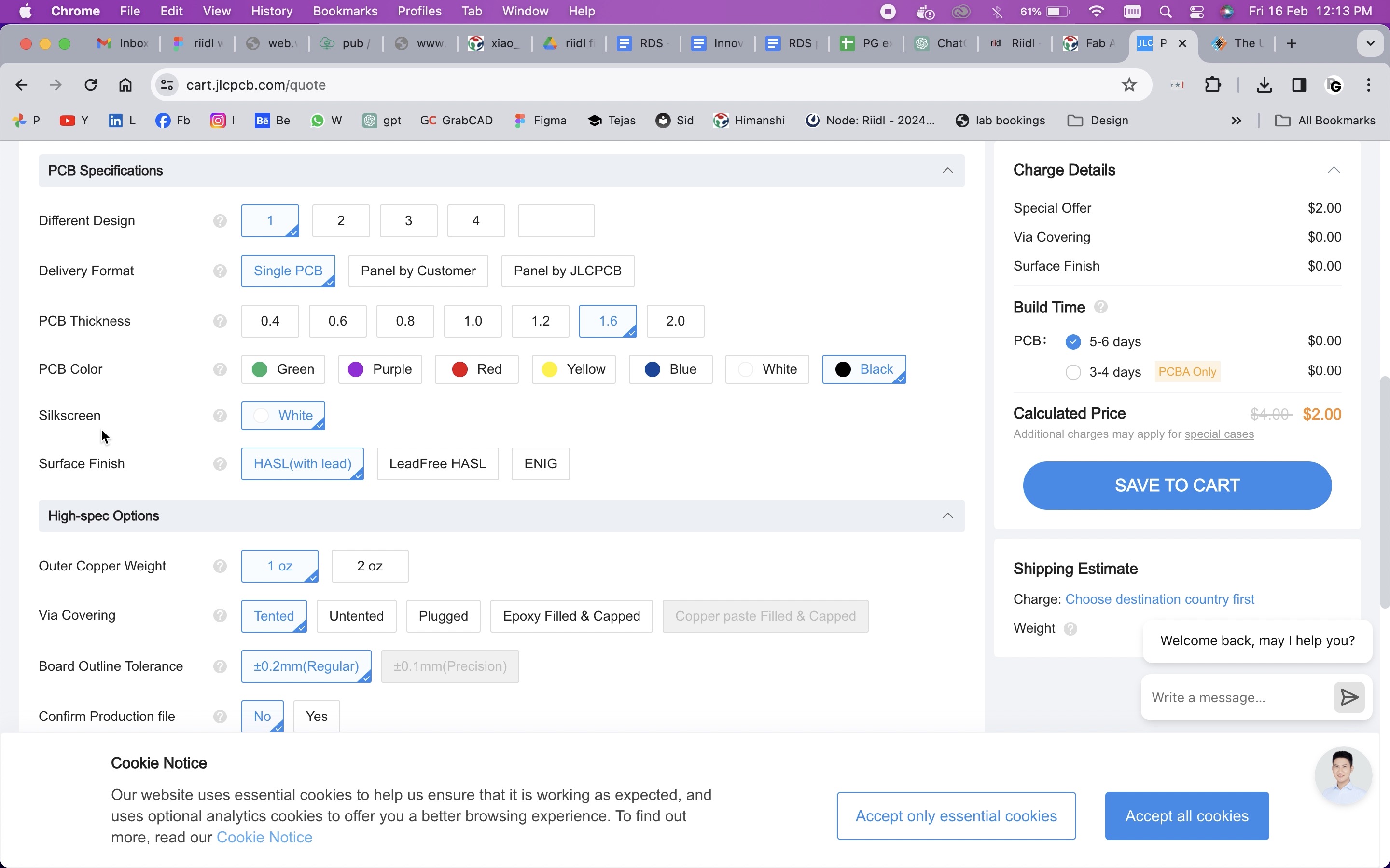
In PCB Specification we selected single PCB
We don't have any pannels. For PCB thickness it guessed the thickness automatically that is 1.6mm and if it does not identifies still make it 1.6mm that is the ideal size don't make it more thin then it has the chances of breaking the PCB.
Then select the colour of your PCB we selected black.
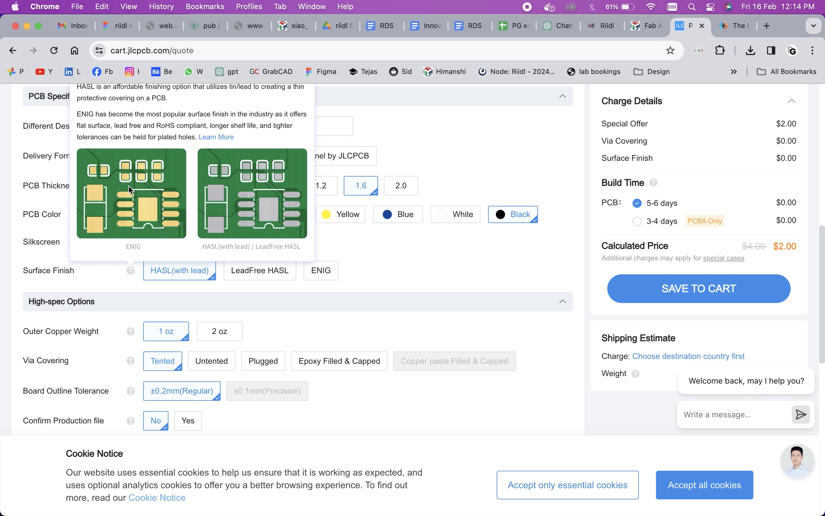
Select any surface finish, ledfree one was expensive so we did not selected that and then we went for a basic normal one that is HASL with lead.
Found one very interesting thing on this website that is if you don't know the meaning of something you can press that and the description window opens which explains that term there itself.
Select outer copper weight, we selected 1 oz
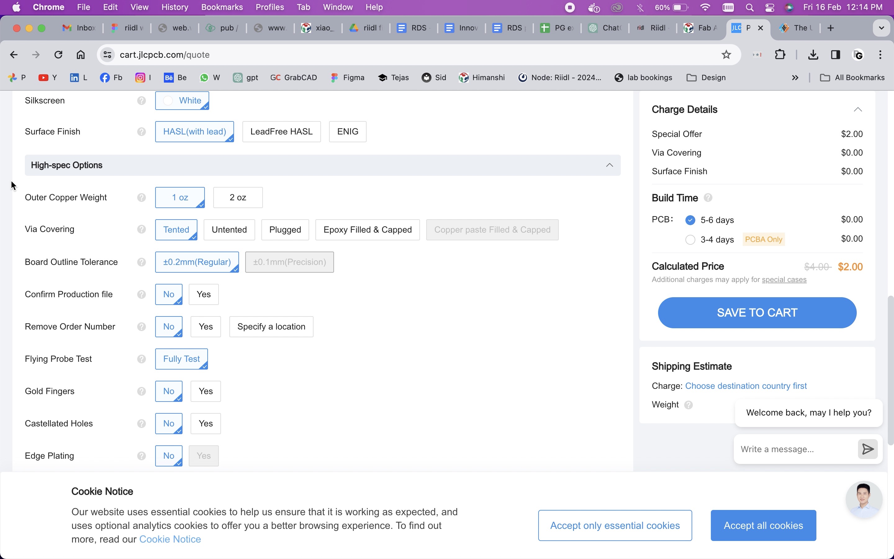
We didn't knew what is via covering so we started raeding the details and then we selected Tented
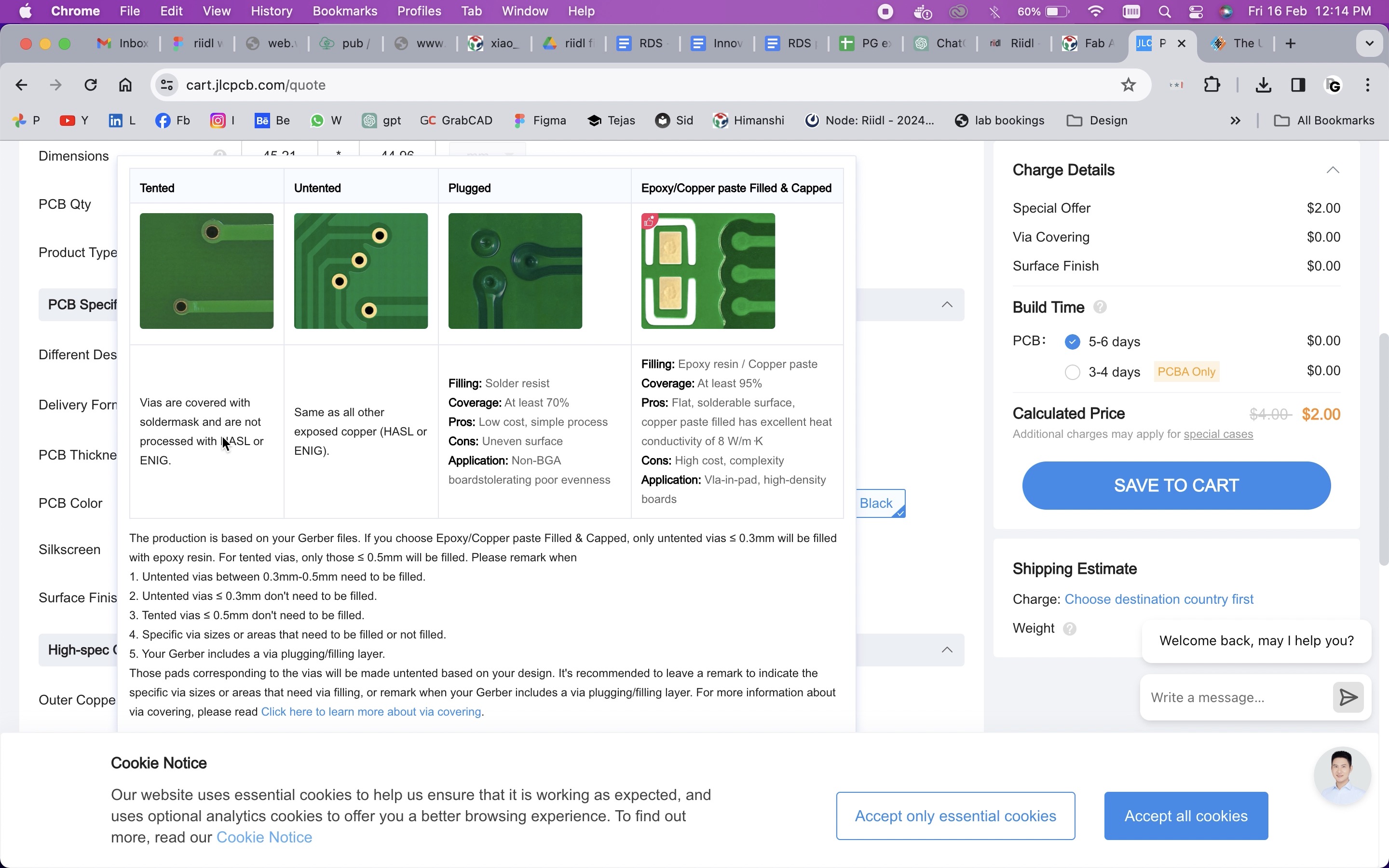
For board outline tolerance we selected regular one.
As we knew our file was perfect so we did not selected yes on confirm production file.
we selected remove order number as JLCPCB will print there order number on that board and we did not wanted that it was unnecessary increasing the cost.
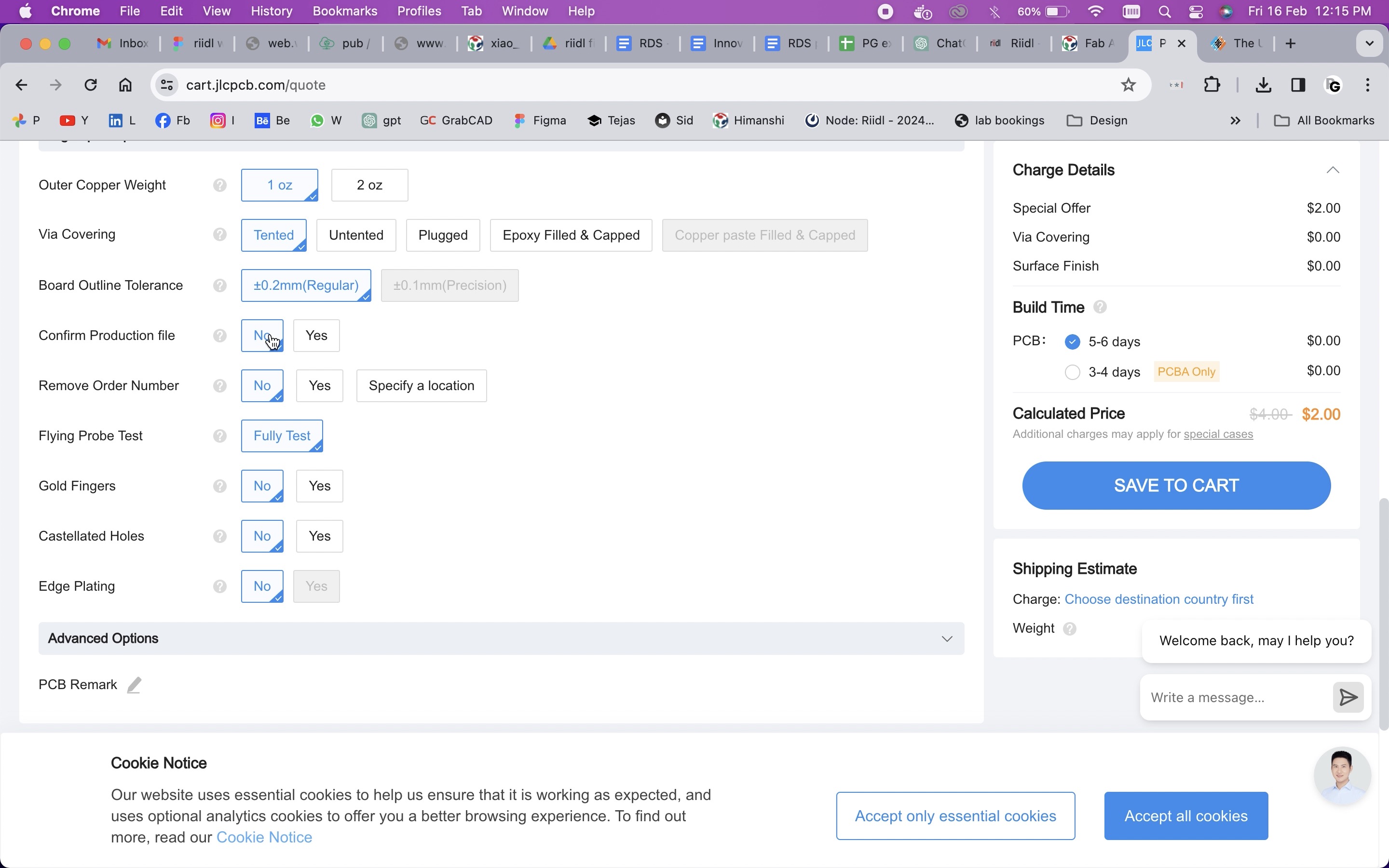
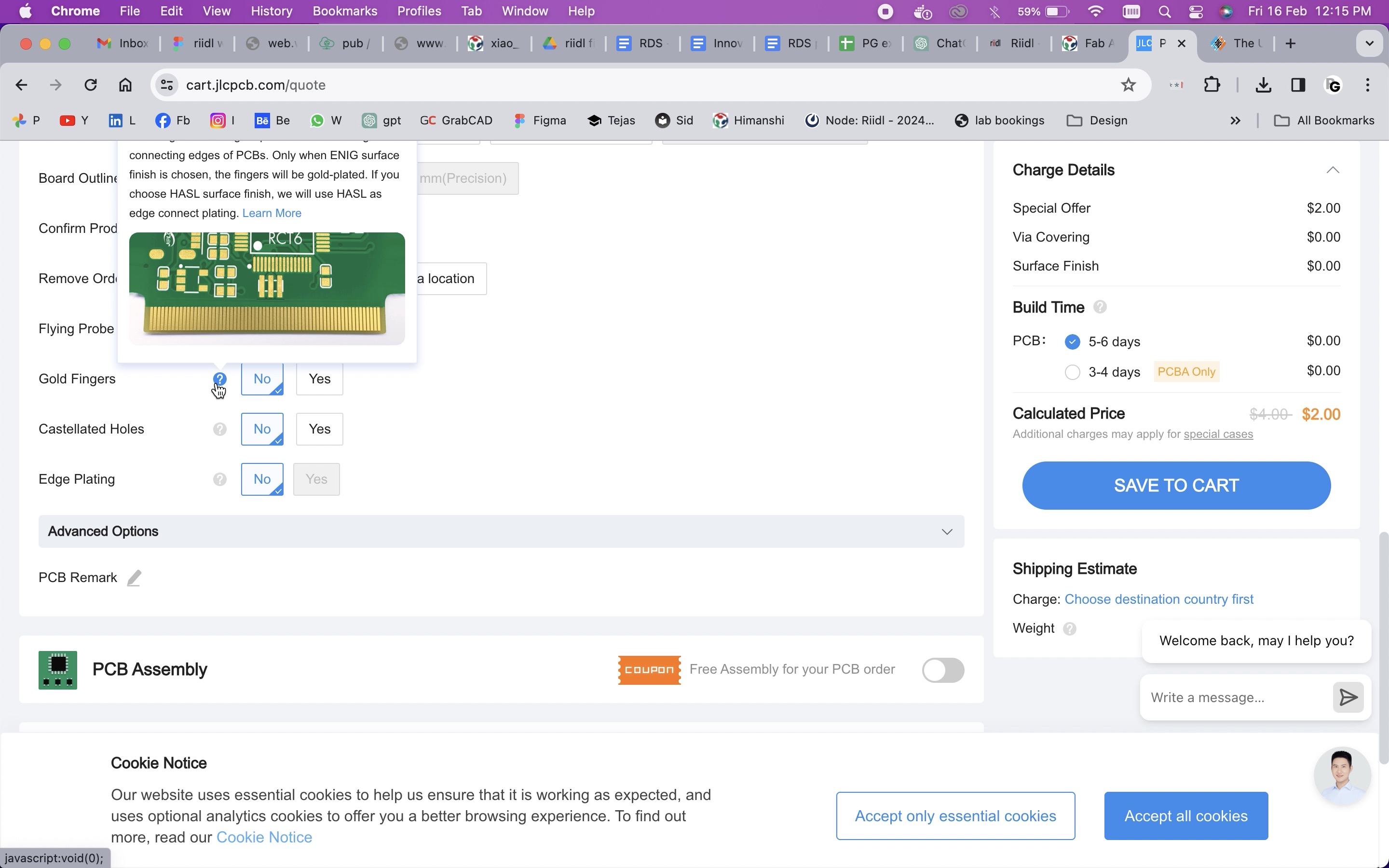
We didn't knew what was the gold finger so we read, it was if we need all wires of the PCB on one side but in our case we don't want that and it also identifies automatically by our file.
We don't want castellated holes as well as edge plating and automatically it again identified by our file.
We don't want assembly because it will solder our components and send the PCB because that was the task we were given to do
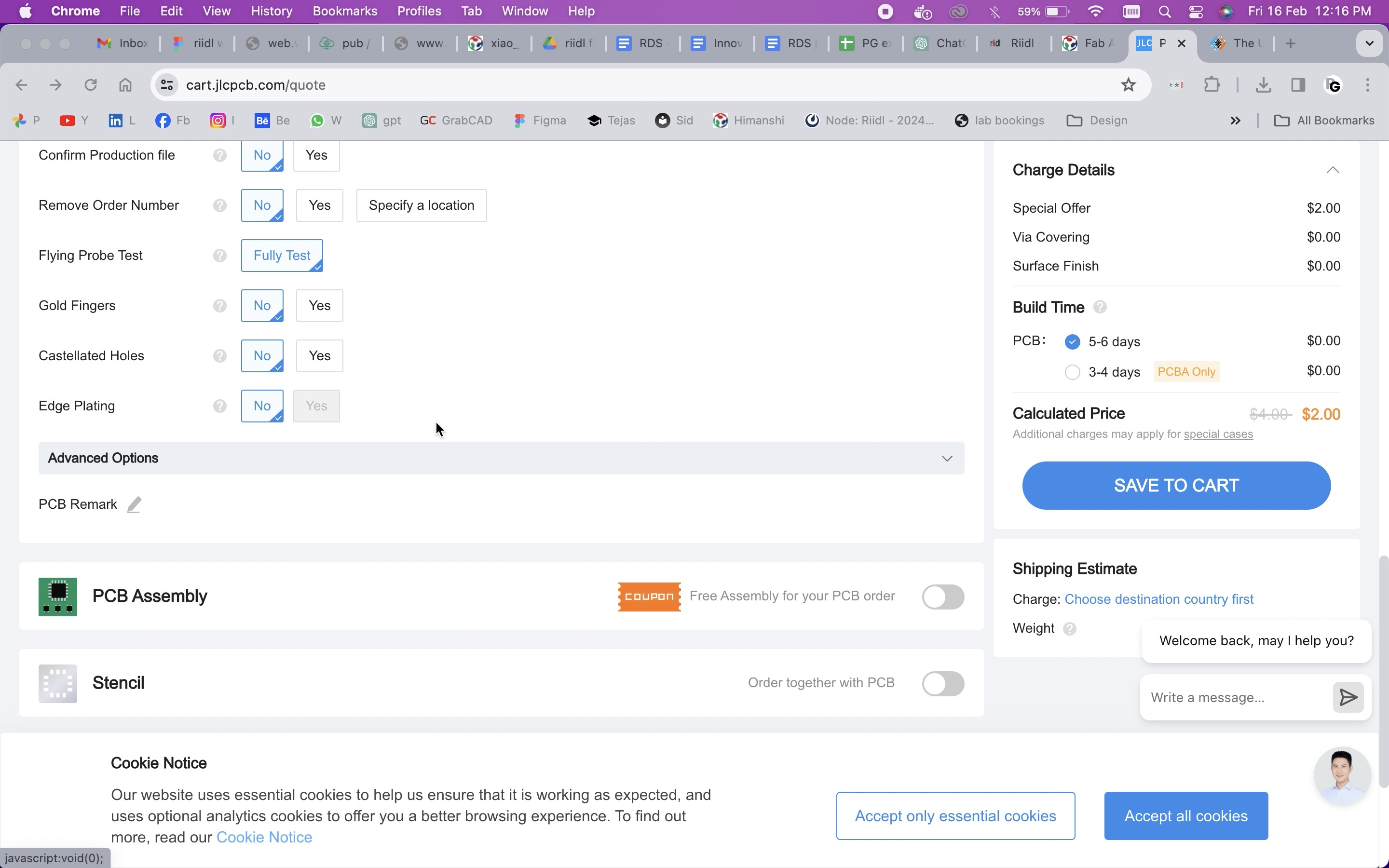
To explore we selected assemble components with PCB then it again asks multiple questions like where do you want to assemble the components on top or bottom
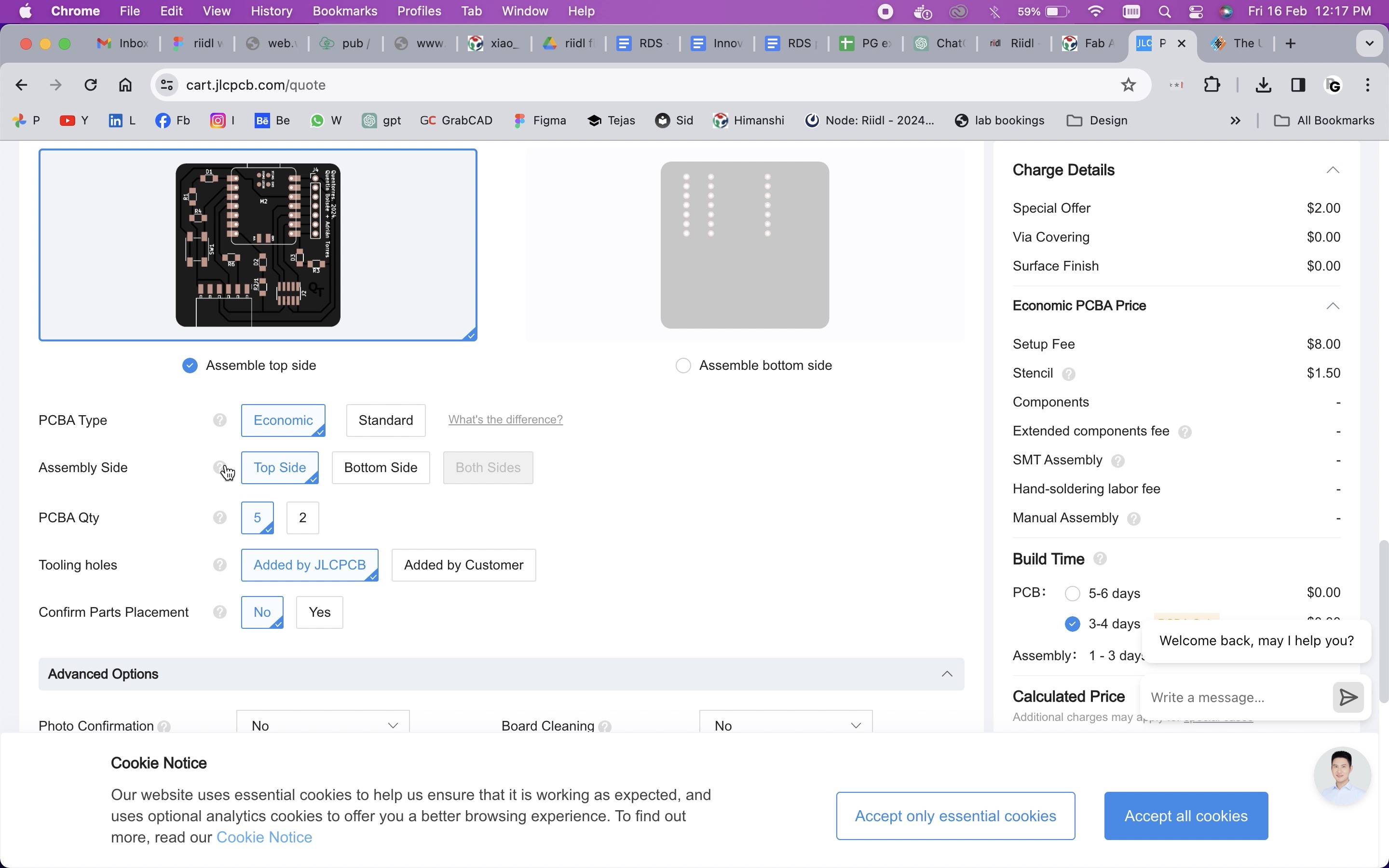
We checked when was the delivery coming and alligned it with rates and then seected checout. This was the entire process of ordering PCB.
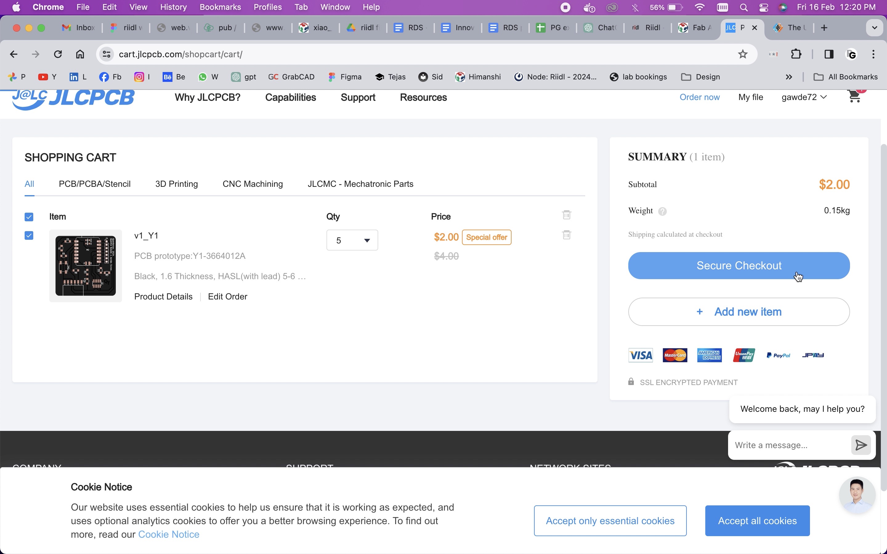
After arrival
Outsourcing from another board house
Vendor 1
As there was problem in our machine we decided to outsource it, So on Friday at 7pmIST we started finding fr vendors as we don't have one. We got 1 vendor he was ready to do it for us and give it us on saturday itself and he told to send the files. He told he will charge rs 200 per sq feet but he wanted dxf file and we had gerber, kicad, and png. So we 3 of us were trying to get dsf file but we failed so in the morning 11:30 when the vendor opened the shop we called him, they did not answer the call and texted us that they will call us right back and they did not call us gain, then I called him again he told that sir is busy and he will connect with y'all after 1:30. So I called him at 3pm she again replied that sir is not yet in the shop. Then they stoppe replying our calls.
Vendor 2
We started searching for another vendors, this vendor told us yes and he told he will gve us the PCB by tuesday and he also stopped answering our call.
Vendor 3
This vendor was nice, he was co=ordinating nicely but he told he will give the PCB in 4-5 days then we thought it will be too late and on monday we can try our old Roland SRM 20 machine and then if it didn't work then we can give him the order.
Vendor 4
We started calling random people by searching on google but some was expensive, some people did not pick our call, some people told 10 working days. This was one vendor who told he will revert on Monday.
So oveerall my experience with sourcing from out was not good it is difficult to co-ordinate with vendors but still I am trying to get 1 vendor for us.
Learnings from group work
In our group work during the electronic production week, we encountered various challenges and underwent a steep learning curve with the PCB machine. Despite meticulous preparation and initial attempts, we faced issues like broken tool tips and improper depth settings, leading to failed PCB milling attempts. Through collaborative troubleshooting and guidance from mentors, we delved into understanding the nuances of machine operation, software setup, and tool calibration. Our persistence paid off as we gradually identified and addressed key issues, such as faulty camera calibration and incorrect milling parameters. By the end of the week, we not only managed to successfully mill a PCB but also gained valuable insights into troubleshooting techniques and the importance of meticulous calibration in electronic production processes.
Conclusion From this Week
During the electronic production week, I embarked on a journey of discovery. As I tried to mill a perfect PCB and solder components, I found myself facing new challenges at every turn. Each attempt taught me something new, whether it was figuring out how the machine works or adjusting settings for better results. Despite facing some initial problems and feeling frustrated at times, the satisfaction of making progress was incredibly rewarding. Through trial and error, I became better at solving problems and gained confidence in tackling unfamiliar tasks. This week helped me grow both technically and personally, showing me the importance of staying resilient and learning from mistakes.
Download Design files
Image Credits
Electronics Production
All images of cover page are credited below:
https://images.app.goo.gl/UMaM7evgmEinf4Wb7.
https://images.app.goo.gl/WmR88dD2jjiNRNWn9
https://images.app.goo.gl/udgx3bfovK9VERZd6
https://images.app.goo.gl/G8DmQ7zMSLwD8R6n6.
https://images.app.goo.gl/7YfxBatesQaRAnW28
https://images.app.goo.gl/sAzsnZKiZRB5c1fM6
https://images.app.goo.gl/8dj622utGZqZTzJb8.
https://images.app.goo.gl/3ddootPVXGrnXwsf6
https://images.app.goo.gl/P5fYgy5mEm85gRQLA
https://images.app.goo.gl/qBa2sB2XoYuQ2sJf8.
https://images.app.goo.gl/XeYAHwBPF5xQYhPL6
https://images.app.goo.gl/KcA9AhRSy6FeVyTQA
https://images.app.goo.gl/vumazahS847JodrB6.
https://images.app.goo.gl/QFdZeWDsh7YGSpDN7
https://images.app.goo.gl/33YdwvVHSvgLgeSPA
https://images.app.goo.gl/aiSsQr2EdBkdkg8W6.
https://images.app.goo.gl/2Wv4d15Xdv4GXTNL6
https://images.app.goo.gl/g6PMtmkZkN16DLgY9