9. Electronics design
Hero Shot
Group assignment:
-
use the Test equipment in your lab to observe the operation of a microcontroller circuit board.
-
send a PCB out to a board house.
Here is a group assignment link
The group assignment link is also embedded below.
Individual assignment
-
Use an EDA tool to design a development board to interact and communicate with an embedded microcntroller, produce it and test it.
-
extra credit: try another design workflow.
-
design a case for it.
-
simulate its operation.
As per assignment requirement to use an EDA in our design, I decided to use KiCad.
Since this is my first time to use KiCad, I had to go through a tutorial on Youtube. And here is the link to watch video
Then I downloaded KiCad software here.
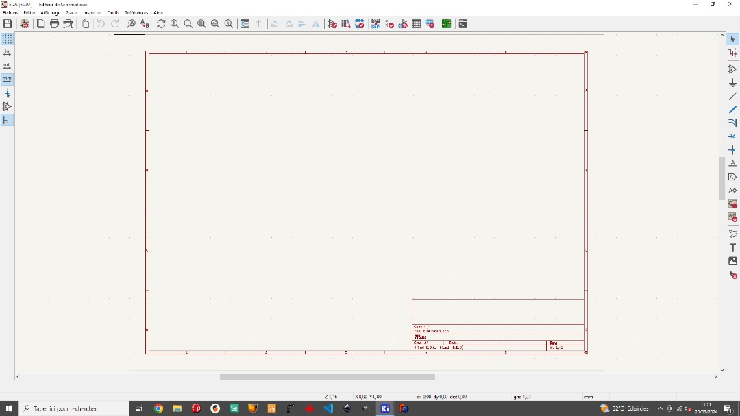
If you open your Kicad this is how it looks

Then I open a new project to start my design.

Libraries
I was instructed to clone the Fabacademy repository so that I get access to all the XIAO footprint and symbols to be used in my design.
Here is a link and steps to do that.
Introduction to Kicad Schematic symbols
To start designing click on the schematic editor symbol below to open your schematic.
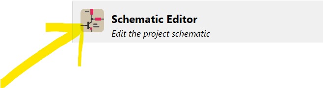
And here you are
Then I started searching and placing components. To do that just click on the symbol below:
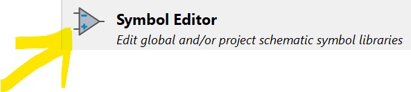
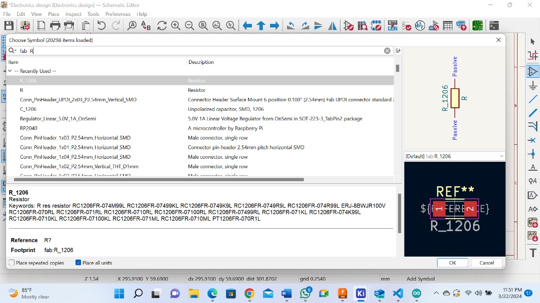
That takes you to the symbol libraries as you can see below. And there you can type and search for any component symbol you want. Scroll up and down to select from different components available on the list. Note that you can only pick one component at a time.
Once satisfied with the component Click OK at the bottom to get the component to your schematic. And just click anywhere on the schematic to drop it down. Highlight it and press M to move it and R to rotate it ino-rder to position it to its location. Press control D to duplicate the component if you want more of the same.
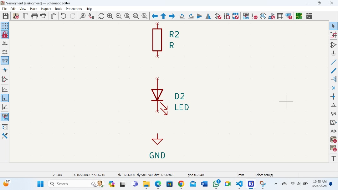
You can see the example how I placed components below.
So, to connect components together you can press on W on your keyboard to add a wire, or click on the Add wire symbol below on your schematic symbol editor.
Beow is an example how I have connected the components.
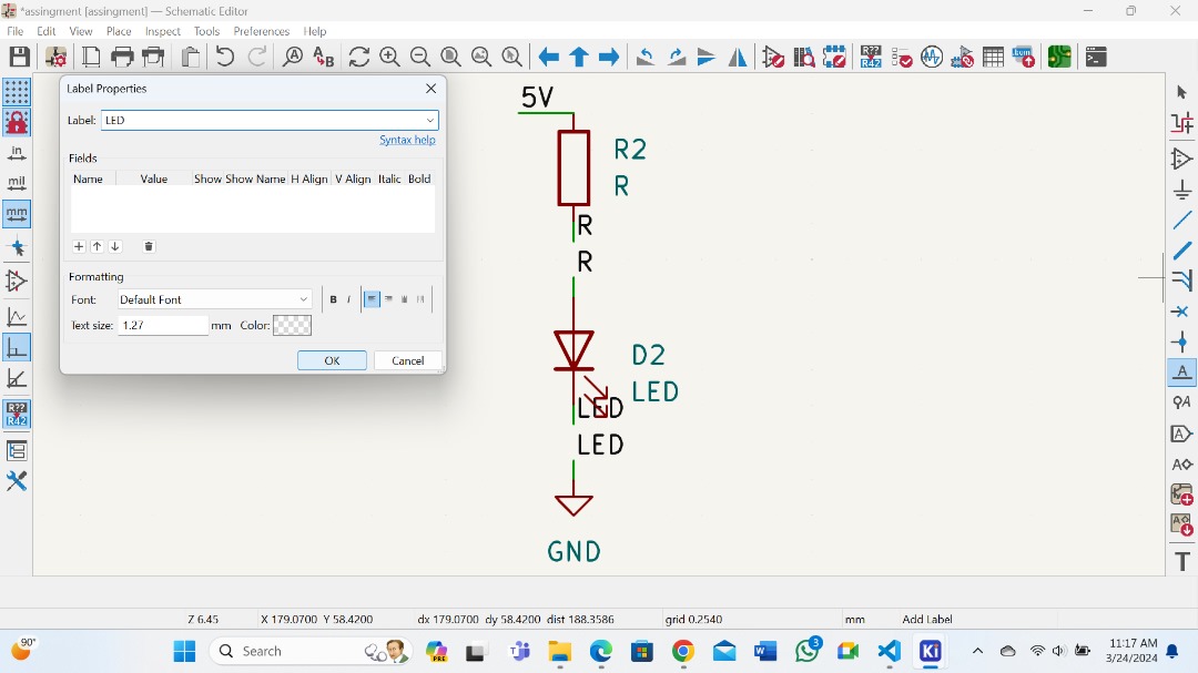
Anonother way of connecting components together is by using labels that can be used to name connection points.
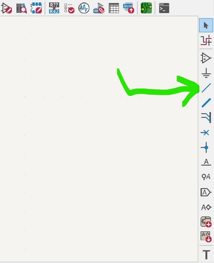
To use labels simply press L on the keyboard or you can click on the I con symbol on the schematic shown below.
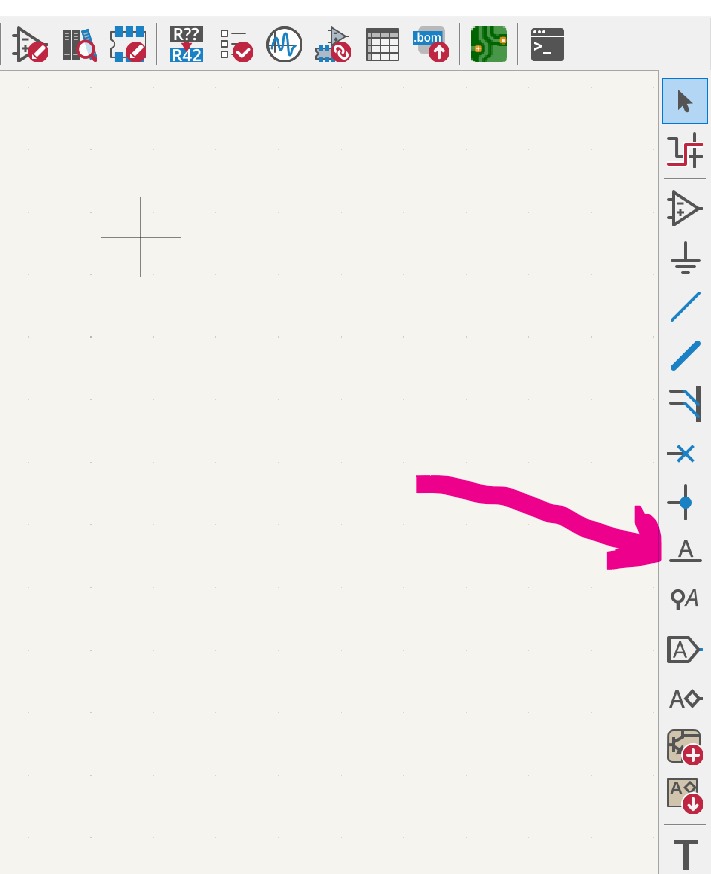
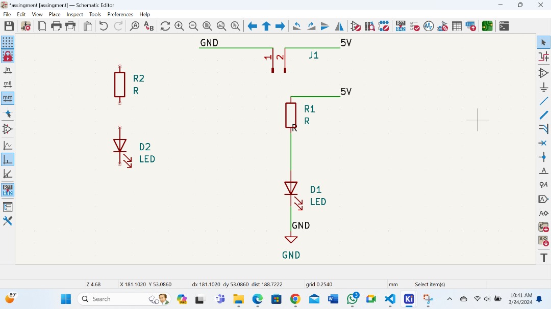
To join the components using net label flags you just have to name the connecting points with the same name eg. RR or LED LED. See below.
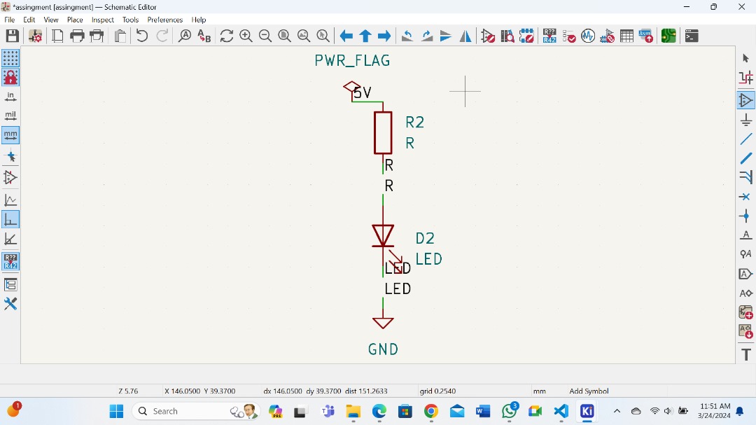
After connecting everything dont forget to click on electrical rules checker. It is also important to add power flags to our circuit as this helps the software to identify where the power is coming from. See below.

Below is how I have connected the power flag
Designing
So, for my design, I decided to use XIAO esp32 C3 and RP2040 Microcontroller since they both have same pinout.
You can find esp32c3 specs here
Below is the pinout of esp32c3

Below is my schematic with all components connected.

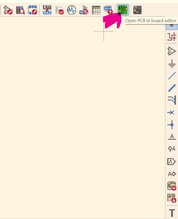
PCB Editor
After finishing with the schematic click on open PCB in board editor symbol shown below.
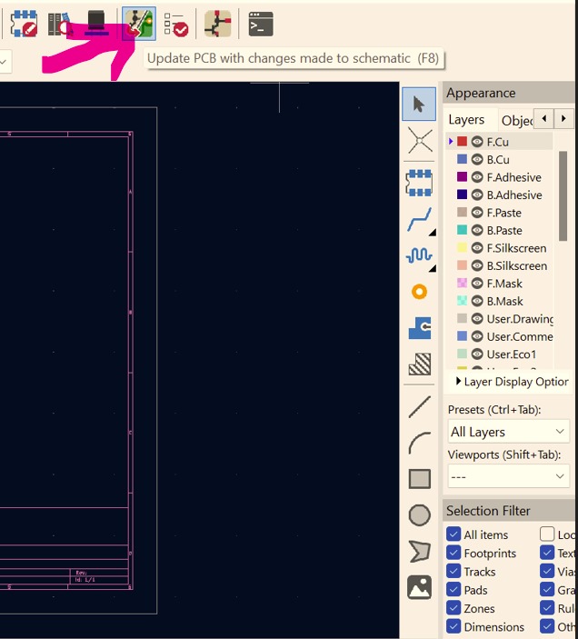
And then click on update PCB with changes made to schematic.
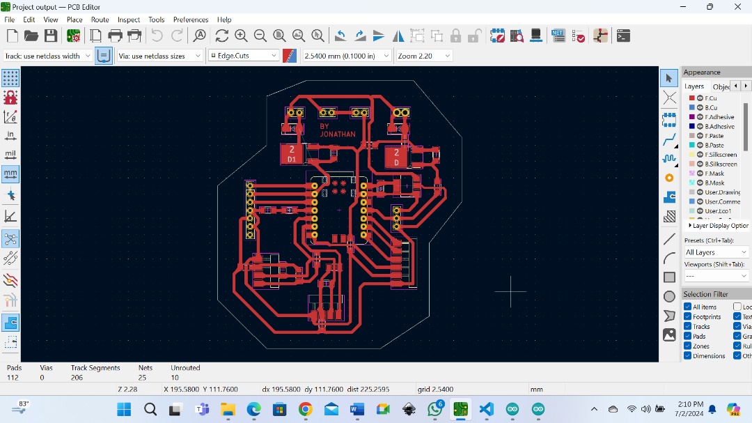
Then finally you can start routing the traces.
Below you can see how the circuit looks like after routing the traces in my Kicad PCB editor window with the components shown in my schematic.
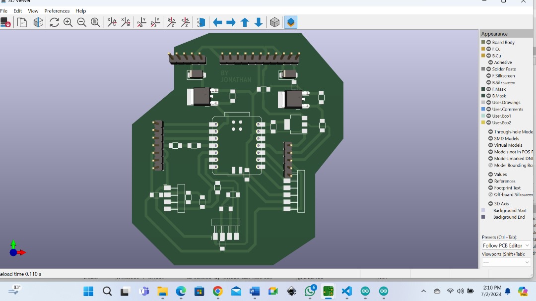
You can click on view 3D viewer Icon on top and see it in 3Dmode as you can see below.
After being satified with the view I can export the file in gerber format for for further processing with a different software.
To do that, go to file>Fabrication Outputs>Gerbers(.gbr)
That will take you to this document below.
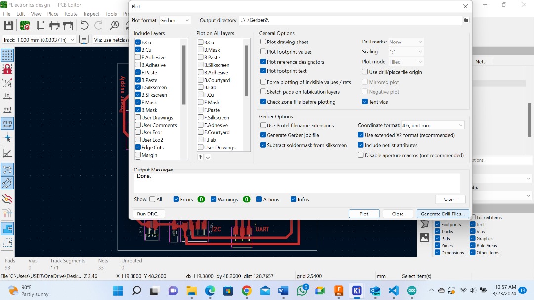
Click on plot to generate your F_cu and Edge_cut gerber file format. Remember to select the output folder for your gerber files. Then get back on the same document and click on generate drill File. That is excellon file for holes.
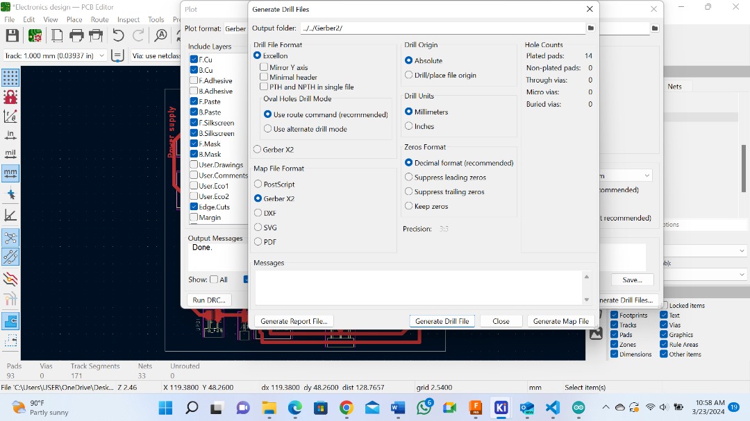
Below you can see I have generated gerber files. But there three important ones that I have circled. For copper traces, Edge cutting and holes. Those are the ones we are going to use for creating G-Code for the cnc machine.
Milling
To proceed with milling processes first we need to create G-Code for our machine.
G-code is a type of computer code that instructs machines on how to perform certain tasks. It is widely used in manufacturing and can control everything from the speed of a machine to the temperature of its heater.
FlatCam
A software that converts Gerber and Excellon (Drill) files to G-Code.
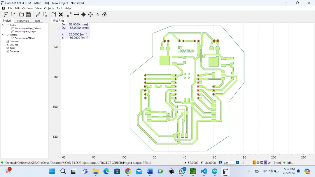
So, open your FlatCam software. Go to file>Ope gerber. That will let you import gerber files to to your flatcam project. And again File>Open Excellon to import the hole file.
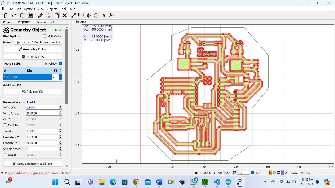
For milling the Traces we used the following sizes.
Tool diameter = 0.33mm, tool depth = 0.08mm, Feed rate = 90mm, spindle speed = 1000, travel Z = 5mm, cut Z =0.08mm.
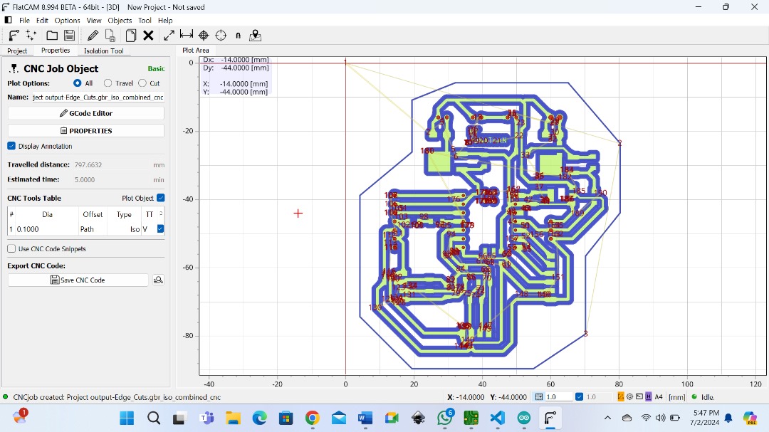
Then after generating the G-Code with FlatCam you export the G-Code for milling processes.
Producing the ciruit board
So, the next step is to mill our circuit board using cnc and in our case we use mini 1610 pro machine.
We use gbr controll candle software to control the cnc machine.
After the production see how it looks below.

Soldering
After milling is complete the next step is to solder components on the board.
According to my circuit design below are the list of components to be soldered to the board.

Now we can solder the components.
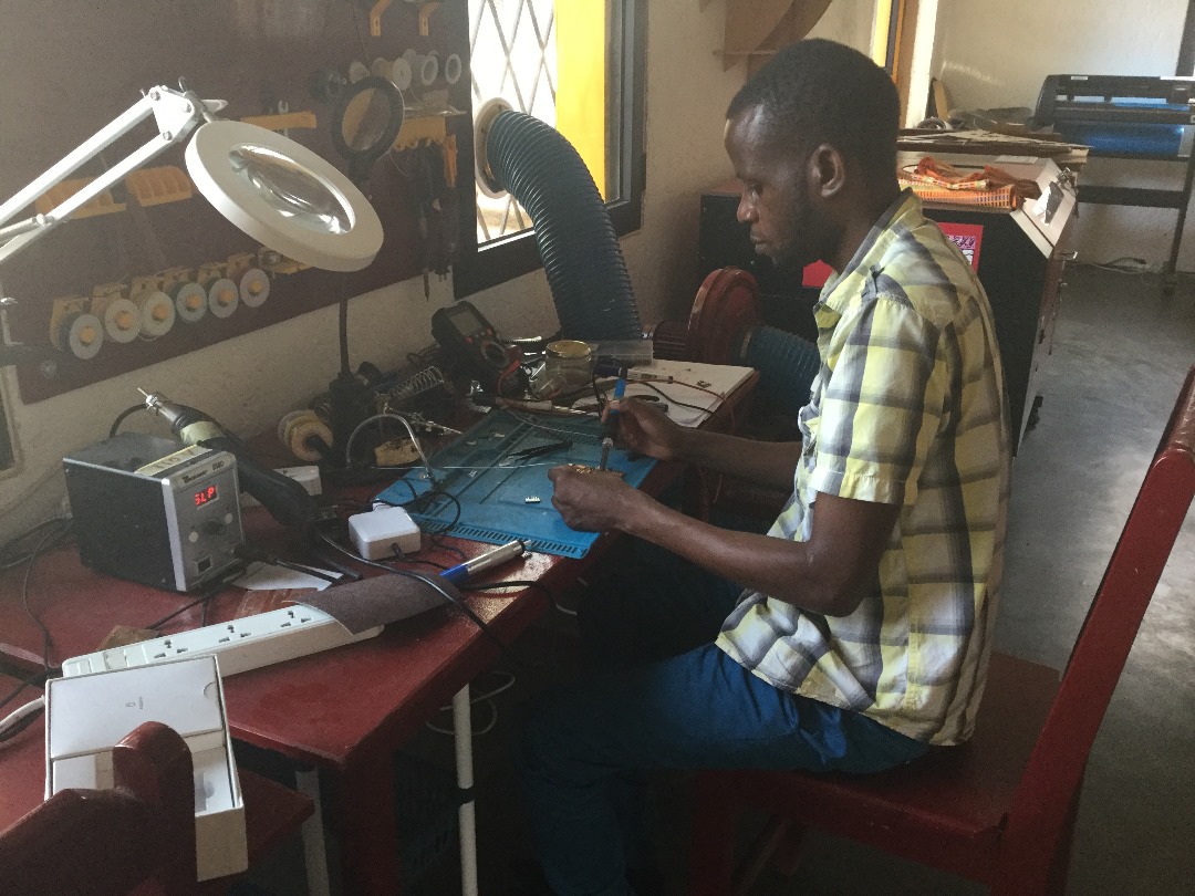

Now finally you can see how it looks after all components have been located and soldered to their respective places.

Programming
Since we were requested to produce and test the board, therefore, we need to install a program and test.
The Micro controller that I am using is compatible with the Arduino IDE. So I am going to use Arduino to program to test it according to how we want it to perform.
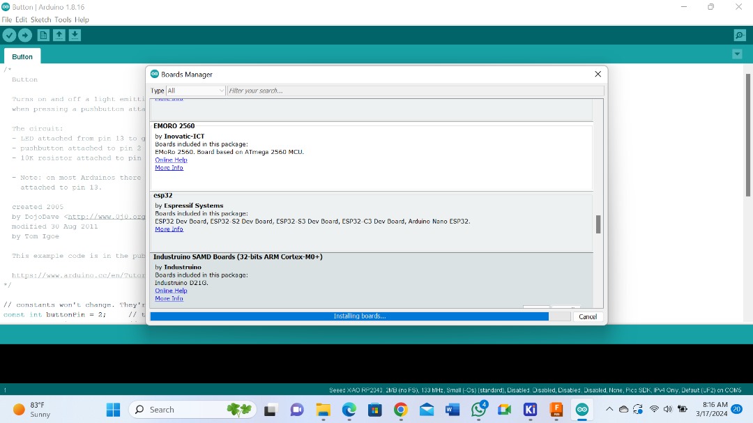
So in my case I have the Arduino already installed during electronics production week, therefore, for now I just need to add my micro controller which is esp32c3 to the board manager.

By going to tools>Boards, you can choose your board among the boards available.
Below you can see my board is available in my Arduino boards.
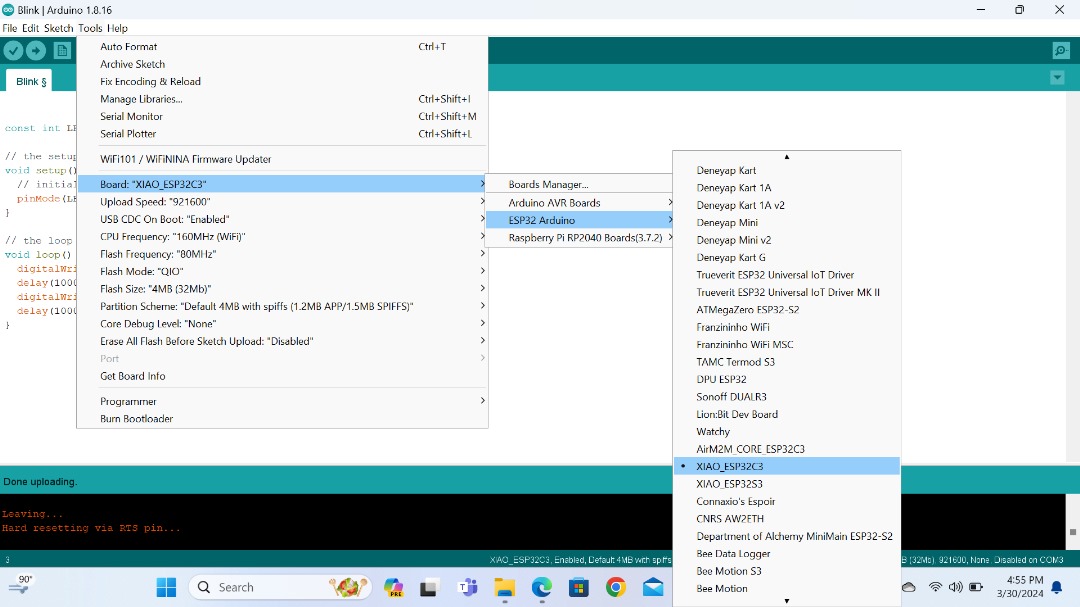
For detailed steps you can refer to electronics production week because we did the same process.
Now to test my board and below is the code.

Here is a clear one

#include <Wire.h>
#include <LiquidCrystal_I2C.h>

LiquidCrystal_I2C lcd(0x27, 16, 2);  // I2C address, num cols, num rows

void setup() {
  Wire.begin();  // Initialize I2C
  lcd.init();    // Initialize LCD
  lcd.backlight();  // Turn on backlight
}

void loop() {

  lcd.clear();  // Clear the LCD at the start of the loop
  for (int i = 0; i < 16; i++) {
    lcd.setCursor(i, 0);  // Move cursor to the right
    lcd.print("Hello World");
    delay(1000);  // Delay for scrolling effect

     lcd.setCursor(i, 1);
    lcd.print("Jonathan Here");
    delay(500);
    lcd.clear();  // Clear the LCD at the end of the loop
  }
  delay(1000);  // Delay before scrolling again
  }
And here we go, “Hello World” “Jonathan Here” is appearing on the screen. That means the board is working just fine.