Hello World Board
Write something at the front
Written on 5.18th, 23:42! I am in in ChaiHuo Lab right now and starting the assignment...
(Actually is written on 5.19th... Cause the board is not working last night...)
But I feel so great, indeed:))))) because I design my very first board! Thanks Salman for the tutoring!
File Sharing
Errors and knowledge learnt
I have faced so many errors and learnt a lot this time... I will start at the very beginning:
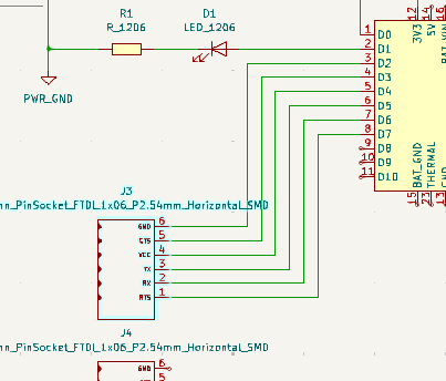
The schematic diagram is really important in the first place!
Before doing the PCB, the schematic diagram designed first is really important. If this is not doing well, the PCB layout will be so confused.
- Like I did before, this is looking great for the schematic, the lines are fine and neat:
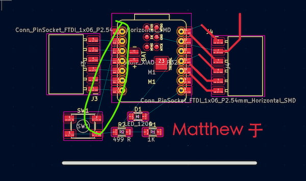
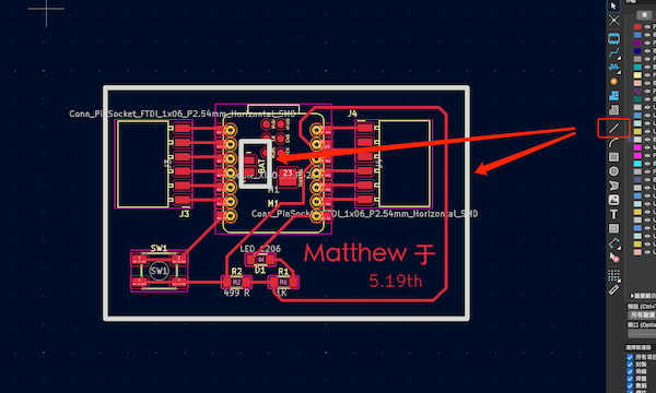
but in the PCB layout the lines will go far from fine:
So when design the schematic diagram, I have to consider the Pinout from the original file and the best solution to put out the lines:
At the same time, I should look back and forth at the schematic and PCB to make sure that the wiring will not jam:
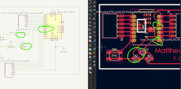
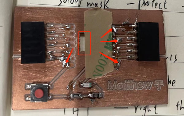
- And another important thing is watching the samples:
This GND is a sample, and the real GND should be also presented:
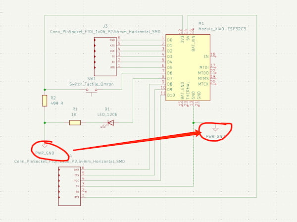
Otherwise... You think the board is fine and you are happy about your board~
But later after you soldering so hard to finish it, you will find it:
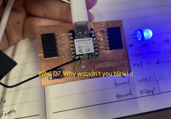
LED not working!
Soldering issues
There are too many issues for my first board soldering:
- Do not put the soldering iron on the copper plate for too long, otherwise will damage the board, copper flaking:
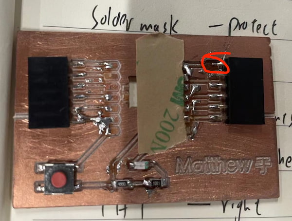
- If I want to use the back hole, I should remember to reserve enough space, otherwise the patch module will be crooked, becoming very difficult to weld, and it would be easy to short circuit:
Solder mask is a great option.
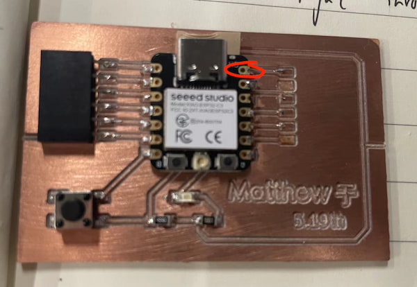
- Sometimes, the connection measured by the meter is OK, but need to solder some more tin to it, because the current may not be enough(the tin is little).
Using my new PCB as an example, here is not enough tin, thus the output is not connected(not enough current/power)
Materials
SMD is on the surface, and THT is right through the hole. For week 4 I am using THT components, they might work but not well looking.
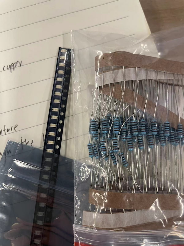
For every functional modules, the capacitance, resistance, and inductance components are necessarily considering and there are some tools for calculating them. Like: LED Risistor Calculator
The Preparation
So for the first I download the Kicad software for my MAC.
And the Fab Academey has provided rich components library on GitLab for KiCAD:
- Download the liarbry and unzip it.
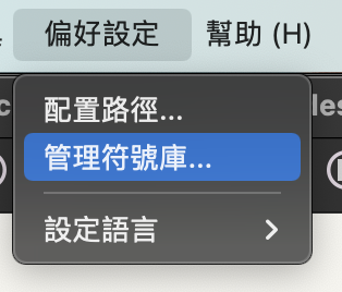
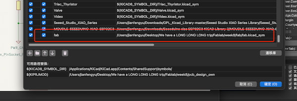
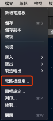
- Then go to "Preferences / Manage Symbol Libraries" and add fab.kicad_sym as symbol library, I'm using the CN version:
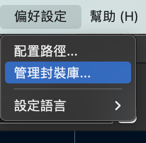
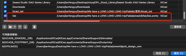
- Finally go to "Preferences / Manage Footprint Libraries" and add fab.pretty as footprint library, I'm using the CN version:
Board Setup
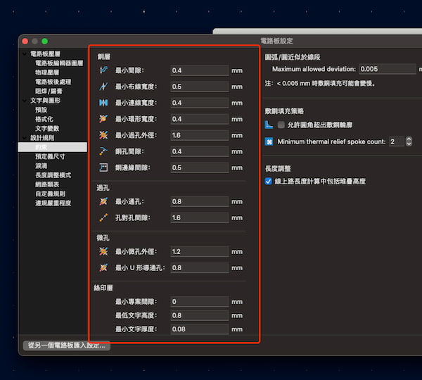
I need to design the board according to the existing machinery, including the wiring setting of the copper layer, the gap, the size of the drill hole and so on.
The right steps
Design on KiCAD
After the preparation, I can start working on my design on KiCAD:
My idea just simple: extend out all the ports of XIAO ESP32C3, and cut a hold for the battery charging.
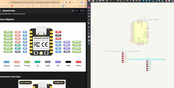
- I first input the schematic diagram of XIAO ESP32C3 in the map:
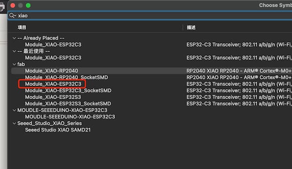
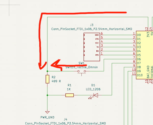
- Then for my requirements, I add one LED, one switch, and two pinsockets(6 pins) from the Fab library. Then referring to the XIAO ESP32 Wiki:
- Then I calculate the circuit and add 1000 ohm resistor connecting to my blue LED nad 499 ohm resistor to my switch.
For adding 499 ohm resistor to the switch, it is because it contents two input and two output, and one side of the circuit needs to be directly grounded, with a resistor to prevent him from short-circuiting and burning out the circuit.
- After done the connection and all seems good, I click the convert to bring all the packages:
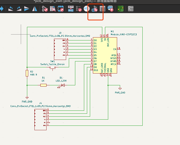
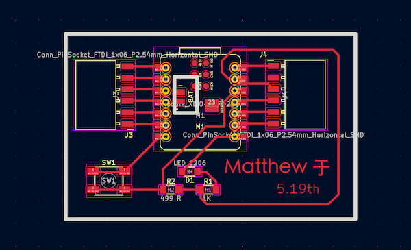
- And done for the layout, and use the "Edge.Cuts" to do the cutting through.
For the text using iron will be fine.
Finally the PCB looks like:
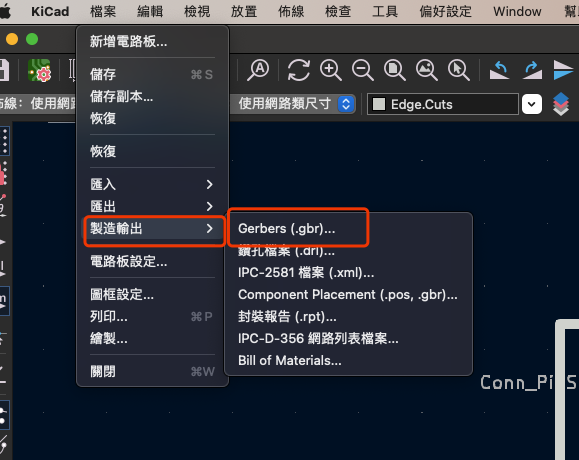
- Then I output the Gerber files:
Board Cutting
Next I should convert the circuit design to my real board.
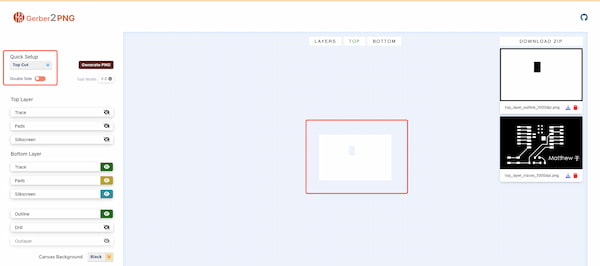
d tI first uploahe Gerber files to Gerber2PNG to generate the PNG file:
"Top Trace":
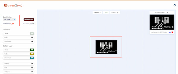
"Top Cut":
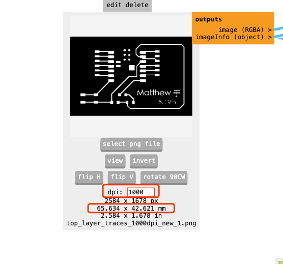
Then I upload the PNG files to the Mods:
Selecting the "dpi" as 1000 first:
and then for the "Trace" using V-bit(0.4mm)
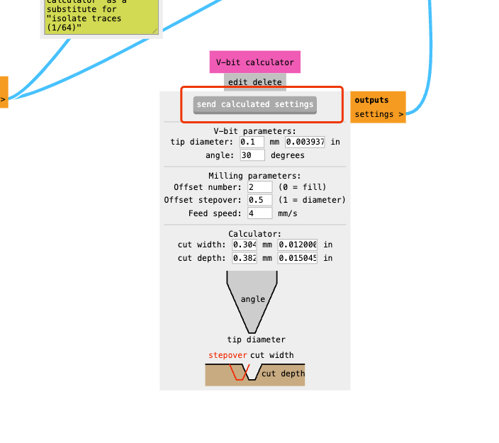
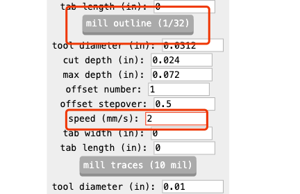
for the "Cut" using 1/32 mill(0.8mm), setting speed as 2mm/s for more using(in case broken)
Watch out the final outcome:
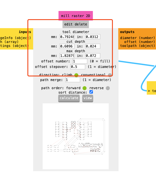
The depth is really important and matter. This is for drill not for the v-bit.
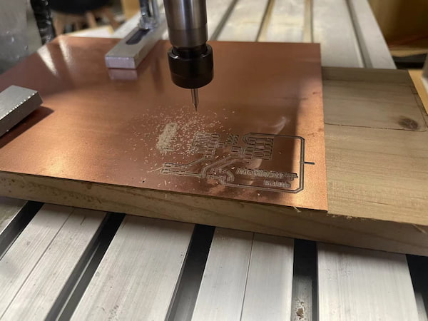
For outputing the G-code files, I can put them into the CNC machine:
Cutting on the computer:
Cutting one the machine:
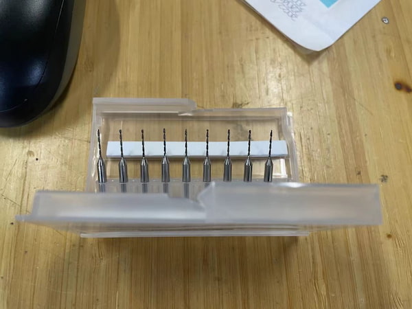
Broken one drill, but not big deal.
Order so many:)))))
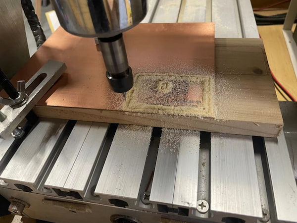
Done:
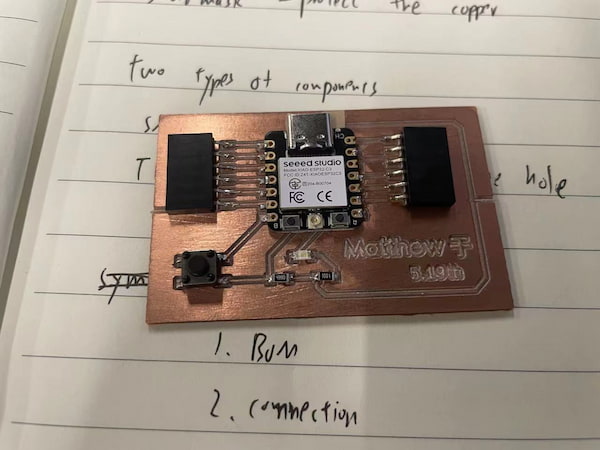
Soldering and testing
I am removing my components from the previous:
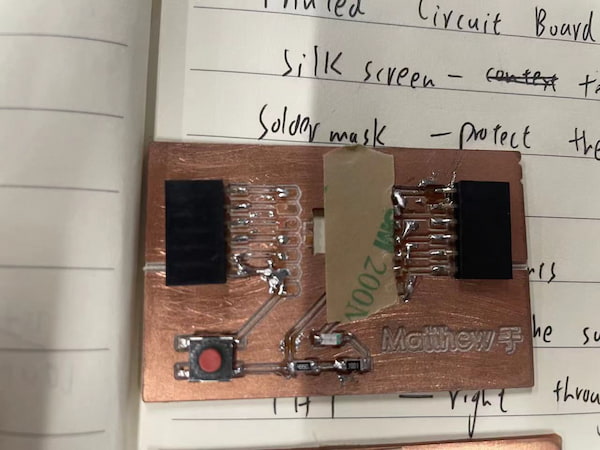
And put them into the new board:
For the testing I write the code below:
const int buttonPin = D6;
const int ledPin = D7;

void setup() {
  pinMode(buttonPin, INPUT);
  pinMode(ledPin, OUTPUT);
}

void loop() {
  int buttonState = digitalRead(buttonPin);

  if (buttonState == HIGH) {
    digitalWrite(ledPin, HIGH);   // 开启 LED
  } else {
    digitalWrite(ledPin, LOW);    // 关闭 LED
  }
}
The final success one: